Stuart I. Wright EDAX-TSL, Draper, Utah
|
|
|
- Arline Joseph
- 5 years ago
- Views:
Transcription

1 Stuart I. Wright EDAX-TSL, Draper, Utah

2 EBSD Probably the Best Measurement in the World Austin Day, Microscopy & Microanalysis, 11, (2005)
3 OIM 3D Introduction to EBSD 3D Data Acquisition Serial Sectioning Practical considerations for EBSD CdTe PV Case Study Conclusions

4 EBSD Electron backscatter diffraction patterns (or EBSPs) are obtained in the SEM by focusing a stationary electron beam on a crystalline sample. The sample is tilted to approximately 70 degrees with respect to the horizontal. The diffraction pattern is imaged on a phosphor screen. The image is captured using a low-light CCD camera. The bands in the pattern represent reflecting planes in the diffracting crystal volume. Thus, the geometrical arrangement of the bands is a function of the orientation of the diffracting crystal lattice.

5 EBSD

6 EBSD

7 EBSD

8 EBSD

9 EBSD


10 EBSD - Hardware Phosphor screen Camera Bellows Slide
11 EBSD Two Main Application Areas Orientation Imaging Microscopy (OIM) Phase Identification 11


12 EBSD Phase ID EBSD EDS Spectrum Fe 2 TiO 4 Candidate Phases Database 12
 Si 13")
13 Phase ID Al(ZrNi) AlTi Al7Cu4Ni Al9(NiFe) Si 13 AlP Al


14 Phase ID Ferrite Austenite Niobium Carbide Chromium Carbide 14
15 EBSD Two Main Application Areas Orientation Imaging Microscopy (OIM) Phase Identification 15


16 Orientation Imaging Microscopy - OIM j 1, F, j 2 In an OIM scan the beam is stepped across the sample surface in a regular grid. At each point the EBSP is captured and automatically indexed and the orientation and other information recorded (such as the quality of the EBSP, an indexing reliability factor, the secondary detector intensity, EDS data...) 16


17 Orientation Maps An Orientation Map is generated by shading each point in the OIM scan according to some parameter reflecting the orientation at each point. A Grain Boundary Map can be generated by comparing the orientation between each pair of neighboring points in an OIM scan. A line is drawn separating a pair of points if the difference in orientation between the points is within a specified range


18 111 Pole Figure and corresponding OIM Map from an Aluminum Thin Film Texture


19 Residual Strain Pattern Quality -Dark regions are strained -Light regions are recrystallized Local Misorientation - Subtle changes in color
 - Angular resolution (~0.")
20 Electron Backscatter Diffraction - Spatial resolution (~20nm) - Angular resolution (~0.3 ) - Automation (~500pps) Specs


")
21 Sample Conditions Plastic Strain Elastic Strain Lattice Distortions (Probe size) Recrystallized Deformed

22 Normalized IQ Normalized IQ Surface Strain Topography Oxidation layers Conductive coating Sample 1 Preparation 0.9 Image Quality vs Coating Thickness 0 Image Quality vs Coating Thickness Coating Thickness (A) Coating Thickness (A) C on Ni Au/Pd on Ni C on Si Au/Pd on Si C on Ni Au/Pd on N C on Si Au/Pd on S 1200 um SiC 1 um Al 2 O um Al 2 O um SiO 2 10 min
23 Atomic Scattering Factor Aluminum Tantalum EBSPs obtained at 1.92s exposure time (no image processing)
24 Microscope Conditions Probe Size (FE vs. LaB 6 vs. Tungsten) Operating Conditions (Current, Voltage, Vacuum) Video Settings (Exposure, gain, contrast & brightness) 0.6nA Beam Current 4.62 Seconds 2.4nA Beam Current 1.56 Seconds 9.45nA Beam Current 0.6 Seconds
25 Microscope Conditions Voltage Effect Probe Size (FE vs. LaB 6 vs. Tungsten) Operating Conditions (Current, Voltage, Vacuum) Video Settings (Exposure, gain, contrast & brightness) Si at 10 kv and 30 kv
 - Voltage Seems")

26 EBSD Spatial Resolution Electron Beam Interaction Volume - Spot Size Current generally increases with increasing spot size - Current ~5nA (1-10nA) - Voltage Seems to effect depth more than lateral resolution 5-30 kv - Material Higher Z materials are better reflectors - Operating Conditions Drift vs. Speed Interaction Volume Average Pattern
27 Serial Sectioning Use of Combined SEM/FIB with EBSD FIB Electron Beam EBSD Camera


28 In-Situ Milling milling strategy: grazing-incidence edge-milling milling strategy: low-incidence surface-milling edge-milling Fe-Si feature has to be at edge large milling areas required to avoid shadowing of EBSD


29 Serial Sectioning SEM View EBSD surface orientation mapping Trenches to avoid shadowing of EBSD detector Platinum Cap to prevent curtaining FIBView Fiducial marks for re-alignment between stage moves. (Atop platinum for improved contrast)
30 Indexing Details Helpful to understand what is happening in the algorithms so an operator can better make adjustments to optimize the results The algorithms between the EBSD vendors differ from each other but the underlying principles are similar.


31 Q. How do we find the bands? Hough Transform


32 y Hough Transform A given pixel in an image could belong to an infinite set of lines. A line can be parameterized by the Hough parameters r and q. Where q describes the angle of the line and r represents the perpendicular distance of the line from the origin. The relationship between the lines passing through a pixel at a coordinate in the image of x, y can be expressed as: r = xcosq + ysinq. This means a point in image space transforms to a sinusoidal curve in Hough space. r i = xcosq i + ysinq i x

 and its")
33 Hough Transform Consider 4 pixels along a line. For each pixel in the line, all possible r values are calculated for q s ranging in values from 0 to 180 degrees using the equation: r = xcosq + ysinq. This produces 4 sinusoidal curves. This curves intersect at a point at a r, q coordinate corresponding to the angle of the line (q) and its position relative to the origin (r). Thus, a line in the pattern space transforms to a point in Hough Space.

34 Hough Transform An entire image can be transformed into Hough Space by building an accumulator array H(r,q) where, for each pixel in the image, all possible r values are calculated for q s ranging in values from 0 to 180 degrees via the equation r = xcosq + ysinq. The intensity value of the pixel at x, y is then added to the bin in the array at each corresponding r, q. (Strictly speaking the Hough Transform only applies to binary images - this adaptation is the Radon Transform).

35 Hough Transform An entire image can be transformed into Hough Space by building an accumulator array H(r,q) where, for each pixel in the image, all possible r values are calculated for q s ranging in values from 0 to 180 degrees via the equation r = xcosq + ysinq. The intensity value of the pixel at x, y is then added to the bin in the array at each corresponding r, q. (Strictly speaking the Hough Transform only applies to binary images - this adaptation is the Radon Transform).


36 Hough Transform
37 Indexing: Bands Triplet Solutions A set of orientations is obtained from a triplet of bands by comparing the interplanar angles against a look-up table. 200 Angle (hkl) 1 (hkl)
38 Indexing: Bands Triplet Solutions Now allow a little bit of wiggle by setting the interplanar angle tolerance to 5 degrees. Let the red angle be measured as 55 degrees, the blue as 59 degrees and the green as 72 degrees. Now, multiple solutions can exist for the triplet. Angle (hkl) 1 (hkl)
39 Indexing: Bands Triplet Solutions For a set of three bands, compare the interplanar angles against the LUT and determine all possible indexing solutions. Solution 1 Solution 2 Solution 3
40 Indexing: Bands Triplet Solutions n # triplets # triplets n! n 3!3! For a given number of bands, n, used for pattern indexing, the number of band triplets is determined by this formula. Typically 7 to 9 detected bands are used for automatic indexing
41 Indexing: Bands Triplet Voting G R Triplet R G Y R G B Solution 1 (V 1 ) X X Solution 2 (V 2 ) Solution 3 (V 3 ) R G M X R Y B X B M R Y M X X R B M G Y B X X G Y M X G B M X Y Y B M X X Total For this set of 5 detected bands, 10 triplet combinations are possible. For each of these 10 triplets, solution V 1 matched. Solutions V 2 and V 3 each matched one triplet only.
42 Indexing: Bands Triplet Voting Fit = 0.26 Solution V 1. Notice how each of the 5 bands match bands in the indexing solution overlay.
43 Indexing: Bands Triplet Voting Fit = 1.30 Solution V 2. Only the red, yellow, and magenta band triplet now match, producing a higher fit value.
44 Indexing: Bands Confidence Index Triplet R G Y R G B R G M R Y B Solution 1 (V 1 ) X X X X Solution 2 (V 2 ) R Y M X X R B M G Y B G Y M G B M X X X X Solution 3 (V 3 ) Y B M X X Total V V2 CI V ideal 1 V ideal n! n 10 1 CI 10 3!3! 0.9 The confidence index, CI, measures the uniqueness of an orientation solution relative to the total number of possible votes.
45 Indexing: Bands Confidence Index


46 Indexing: Deconvoluting Patterns


47 Indexing: Deconvoluting Patterns & CI
48 Optimizing EBSD Speed - Pretty patterns vs. scanning patterns - Camera Binning Gain - Image Processing - Hough Settings Convolution Mask dtheta Speed vs. Quality - Indexing success rate - Precision - Clean-up


49 Pretty Pictures

50 Reality
51 CCD Camera Binning 1x1 480x480 4x4 120x120 5x5 96x96 6x6 80x80 8x8 60x60 10x10 48x48
52 How Binning Works Binning reduces the number of pixels in the final image, and increases the effective image intensity.
53 CCD Camera Binning 4x4 5x5 6x6 8x8 10x10 1x1 Maximum Frame Rate (FPS) 4x4 (128x128) 543 5x5 (96x96) 640 6x6 (80x80) 732 8x8 (60x60) x10 (48x48) 1000 Faster camera frame rates are possible with binned images.
54 Precision vs. Binning
55 Indexing Rate vs. Binning
56 Camera Gain Minimum Gain 2.76 Seconds Mid-Range Gain 0.55 Seconds Maximum Gain 0.15 Seconds As gain goes up, exposure time goes down, however, the signal to noise ratio decreases.
57 1x1 Binning (480x480 Pixels) 0% Gain 20% Gain 40% Gain 60% Gain 80% Gain
58 5x5 Binning (96x96 Pixels) 0% Gain 20% Gain 40% Gain 60% Gain 80% Gain
59 10x10 (48x48 Pixels) 0% Gain 20% Gain 40% Gain 60% Gain 80% Gain
60 5x5 (96x96 Pixels) Spread & Indexing Rate 0% Gain 20% Gain 40% Gain 60% Gain 80% Gain Orientation Spread Indexing Success Rate % 100% 97.1% 24.8% 0.8%
61 SEM Settings Beam Current 0.6nA Beam Current 4.62 Seconds 2.4nA Beam Current 1.56 Seconds 9.45nA Beam Current 0.6 Seconds Note however that the gain required for an EBSD pattern is inversely related to the amount of incident beam current.


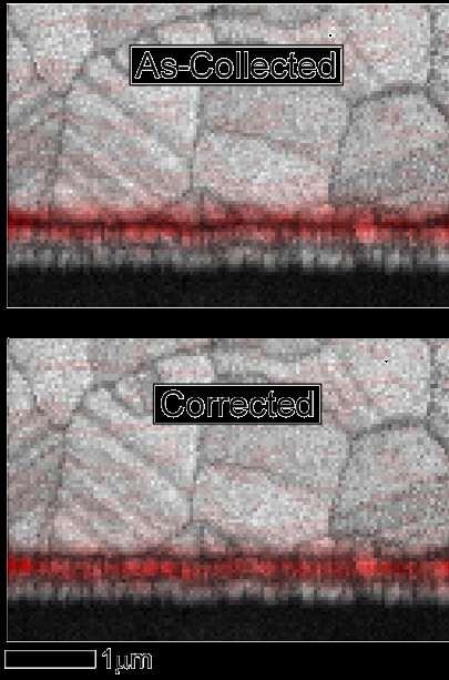
62 Image Processing Low enough magnification to get at least 25 grains with TV rate scanning We usually have to do some image processing of the patterns to get uniform intensity across the pattern so that the automated band detection algorithms can do a good job.

63 Dynamic Background Correction Blur Helpful for single crystals or very rough surfaces or also for multiphase samples where the individual phases produce patterns with very different intensity. Any defects in the phosphor screen remain. Slower than static background correction. Both can be used together.

64 Other Image Processing Other image processing can be done as well but this tends to slow the whole process down and generally isn t necessary to get good indexing and band detection.
65 5x5 (96x96 Pixels) With Frame Averaging 0% Gain 40% Gain 80% Gain 0% Gain Avg 40% Gain Avg 80% Gain Avg

66 Hough Transform Raw Hough Transform After convolution with Butterfly Mask


67 Hough Transform One weakness of the butterfly mask is that it enhances peaks from bands a given width. It can be difficult to find the right size of mask when there is considerable variance in the width of the bands as is often the case in low-symmetry materials. This also biases any band width measurements. No Mask Medium Mask (9x9) Small Mask (5x5) Large Mask (13x13)
68 Mask Size & Band Width Voltage Binning

69 Hough Theta Step
70 5x5 (96x96 Pixels) Average Orientation Spread 0% Gain 20% Gain 40% Gain 59% Gain Max FPS 60% Gain 80% Gain 0.5 θ θ θ θ Less than 60% gain is necessary for maximum FPS
71 10x10 (48x48 Pixels) Orientation Spread 0% Gain 20% Gain 40% Gain 41% Gain Max FPS 60% Gain 80% Gain 0.5 θ NA 1 θ NA 2 θ NA 3 θ NA Near 40% gain is necessary for maximum FPS
72 10X10 Points Correctly Indexed 0% Gain 20% Gain 40% Gain 41% Gain Max FPS 60% Gain 80% Gain 0.5 θ 100% 100% 96.7% 97.4% 28.7% 0.9% 1 θ 100% 100% 97.1% 95.3% 24.8% 0.8% 2 θ 100% 99.9% 93.1% 92.2% 12.1% 0.7% 3 θ 100% 99.1% 72.7% 75.2% 3.9% 0.8%
73 Summary and Conclusions High frame rates are achieved through camera binning and camera gain settings. Hough settings must be optimized for a given camera setting. Set up Hough parameters for patterns obtained under scan conditions, not for patterns obtained in a high quality pattern mode. There is a trade-off between speed and orientation precision but not as severe as one might assume. Trust the Hough! Evaluate the quality of the results on the quality of the scan data not how the pattern looks. Note that these results have been shown in diamond cubic silicon and FCC nickel. Non-cubic patterns may require higher resolution, to achieve accurate band detection. Recently submitted a manuscript on precision with a particular focus on precision at grain boundaries.
74 Confidence Index Partitioning or Filtering CI>0.3 We can filter the data based on CI or Fit or other metrics to mask data we do not have confidence in from our subsequent analysis. However, some of these low CI points are actually valid orientations. How can we recover them?
75 Initial Confidence Index Distribution
76 Confidence Index Standardization

77 Confidence Index Standardization With this routine we recover a portion of the data with a low CI value but with the correct orientation. With CI=0, 40% of the indexing is still correct No orientation values are changed.
 routine identifies the maximum fraction of correctly indexed")
78 Confidence Index Standardization As-collected CI> % Grain CI Standardization CI> % The confidence index standardization (CIS) routine identifies the maximum fraction of correctly indexed points. Use it always.
79 Grain Dilation This clean up method is an iterative method. The routine only acts on points that do not belong to any grains; yet have neighboring points, which do belong to grains. A point may not belong to any grain due to the point either not being indexed or due to it belonging to a grain group having fewer members than the Minimum Grain Size. If the majority of neighbors of a particular point belong to the same grain then the orientation of the particular point is changed to match that of the majority grain - otherwise the orientation is randomly changed to match any of the neighboring points, which belong to grains. This process is repeated until each point in the data set becomes a member of a grain. (Alternatively, the user may set the code to only perform a single iteration.) In the schematic below, in the left hand figure the data point in white is not part of any grains. After dilation it's orientation is changed to match that of the neighboring member of the green grain with the highest CI.


80 Grain Dilation 1 Iteration % +4.1% CI > % 3 Iterations % +4.2% 2 Iterations % +4.2%


81 Grain Dilation Grain Dilation can actually work too well. Plausible microstructures can be generated out of nearly random data. Full Grain Dilation Cleanup
82 Summary There are a wide range of tools available to identify the correctly indexed points and remove noise within the data maps. The Grain CI Standardization feature should always be used in conjunction with a CI filter to determine indexing quality. Cleanup routines should be used with care to improve data quality and results and not introduce artificial data. It is good practice to report the cleanup used during analysis and the fraction of points cleaned. Start with the best data possible!
83 Case Study
84 Photovoltaic Materials Energy demand and prices are expected to increase and the demand for alternative sources is high. Photovoltaic thin film solar cells provide a commercially viable technology. Thin film photovoltaic devices use only a small fraction of the raw material when compared to traditional cells. Polycrystalline CdTe and CIGS thin films have higher efficiencies than single crystal devices. The performance of these thin films is influenced by the crystallographic structure, grain boundary character, and grain size. CdTe CdS In 2 O 3 Glass
85 Photovoltaic Materials Cadmium Telluride - Cubic (FCC) Cadmium Sulfide - Cubic (FCC) - Hexagonal Indium Oxide - Cubic (FCC) Tin Oxide - Tetragonal Silicon Oxide - Trigonal SnO CdTe CdS In 2 O 3 Glass (SiO 2 )

![Cubic (Oh) [m3m] Indexed](/docs-images/83/88379731/images/86-1.jpg "as CdTe Indexed as In 2")
86 Phase Differentiation Challenges EBSD pattern Cubic (Oh) [m3m] Indexed as CdTe Indexed as In 2 O 3
 Tin Oxide - Tetragonal Silicon Oxide - Amorphous SnO CdTe CdS In 2 O 3 Glass (SiO 2")
87 Photovoltaic Materials Cadmium Telluride - Cubic (FCC) Cadmium Sulfide - Cubic (FCC) - Hexagonal Indium Oxide - Cubic (FCC) Tin Oxide - Tetragonal Silicon Oxide - Amorphous SnO CdTe CdS In 2 O 3 Glass (SiO 2 )
88 EBSD Phase Mapping Gold - Cubic (FCC) Cadmium Telluride - Cubic (FCC) Cadmium Sulfide - Cubic (FCC) - Hexagonal Indium Oxide - Cubic (FCC) Tin Oxide - Tetragonal Silicon Oxide - Trigonal

89 EDS RGB Element Mapping S CdS Cd CdTe Te

90 EDS Phase Mapping
91 EDS Phase Mapping Gold Cadmium Telluride Cadmium Sulfide Tin Oxide Indium Oxide Silicon Oxide

92 Chemistry assisted indexing

93 Chemistry assisted indexing - Notes Using the counts of individual elemental ROIs is faster than using full spectral analysis and is effective and efficient on these materials. Need to resolve intermediary phases High-Tilt EDS

")
94 EBSD & EDS phase mapping In 2 O 3 CdS (Hexagonal) CdTe
95 EDS at EBSD Geometry Azimuthal Angle ( ) Sample Tilt ( ) CPS (Normalized) NA Tilting the specimen increases the EDS count rate due to reduced absorption The improved count rate is often beneficial for simultaneous EDS-EBSD mapping


96 Effect of Working Distance on EDS Signal For simultaneous EDS and EBSD data collection, both detectors need to be aimed at the same working distance. EBSD data is often collected away from the optimal EDS analytical working distance depending on the sample size and geometry A special EDS electron trap was designed to allow EDS detection over an extended WD range.
97 Detected EDS fraction EDS Detection Improvement SEM working distance
98 Detected EDS fraction EDS Detection Improvement SEM working distance
99 ezaf Quantification Results RMS (%) Fe ZAF ezaf Significant improvement for difficult sample compared to old ZAF routine

100 EBSD and EDS interaction volumes

101 EDS and EBSD Interaction Volume

102 EDS and EBSD Interaction Volume

103 EBSD and EDS interaction volumes
 Data")

104 3D Reconstruction Phase map (EDS) Data collected on a Zeiss Ariga with the help of Hubert Schulz

105 3D Reconstruction Orientation Map (EDS + EBSD)


106 Thank you for your attention
EBSD Basics EBSD. Marco Cantoni 021/ Centre Interdisciplinaire de Microscopie Electronique CIME. Phosphor Screen. Pole piece.
 EBSD Marco Cantoni 021/693.48.16 Centre Interdisciplinaire de Microscopie Electronique CIME EBSD Basics Quantitative, general microstructural characterization in the SEM Orientation measurements, phase
Observation in the GB (Gentle Beam) Capabilities
 Capabilities") A field-emission cathode in the electron gun of a scanning electron microscope provides narrower probing beams at low as well as high electron energy, resulting in both improved spatial resolution and
A field-emission cathode in the electron gun of a scanning electron microscope provides narrower probing beams at low as well as high electron energy, resulting in both improved spatial resolution and
Carnegie Mellon MRSEC
 Carnegie Mellon MRSEC Texture, Microstructure & Anisotropy, Fall 2009 A.D. Rollett, P. Kalu 1 ELECTRONS SEM-based TEM-based Koseel ECP EBSD SADP Kikuchi Different types of microtexture techniques for obtaining
EBSD Electron BackScatter Diffraction Principle and Applications
 EBSD Electron BackScatter Diffraction Principle and Applications Dr. Emmanuelle Boehm-Courjault EPFL STI IMX Laboratoire de Simulation des Matériaux LSMX emmanuelle.boehm@epfl.ch 1 Outline! Introduction!
Introduction to Electron Backscattered Diffraction. TEQIP Workshop HREXRD Feb 1 st to Feb 5 th 2016
 Introduction to Electron Backscattered Diffraction 1 TEQIP Workshop HREXRD Feb 1 st to Feb 5 th 2016 SE vs BSE 2 Ranges and interaction volumes 3 (1-2 m) http://www4.nau.edu/microanalysis/microprobe/interact-effects.html
Crystallographic Textures Measurement
 Crystallographic Textures Measurement D. V. Subramanya Sarma Department of Metallurgical and Materials Engineering Indian Institute of Technology Madras E-mail: vsarma@iitm.ac.in Macrotexture through pole
Multiphase analysis - combining EDS and EBSD
 Multiphase analysis - combining EDS and EBSD Outline Review: Conventional materials characterisation: Analysing polyphase materials using EDS Analysing polyphase materials using EBSD Combined EDS and EBSD
In-situ Heating Characterisation Using EBSD
 Webinar In-situ Heating Characterisation Using EBSD Speakers Dr. Ali Gholinia Dr. Neil Othen Dr. Jenny Goulden Topics Introduction to EBSD Why do in-situ experiments? EBSD equipment requirements for in-situ
Fundamentals of X-ray diffraction and scattering
 Fundamentals of X-ray diffraction and scattering Don Savage dsavage@wisc.edu 1231 Engineering Research Building (608) 263-0831 X-ray diffraction and X-ray scattering Involves the elastic scattering of
ORIENTATION DETERMINATION BY EBSP IN AN ENVIRONMENTAL SCANNING ELECTRON MICROSCOPE
 Pergamon PII S1359-6462(99)00086-X Scripta Materialia, Vol. 41, No. 1, pp. 47 53, 1999 Elsevier Science Ltd Copyright 1999 Acta Metallurgica Inc. Printed in the USA. All rights reserved. 1359-6462/99/$
AN INTRODUCTION TO OIM ANALYSIS
 AN INTRODUCTION TO OIM ANALYSIS Raising the standard for EBSD software The most powerful, flexible, and easy to use tool for the visualization and analysis of EBSD mapping data OIM Analysis - The Standard
Electron Microscopy Studies of Niobium Thin Films on Copper
 Electron Microscopy Studies of Niobium Thin Films on Copper Roy Crooks 1, Greg Thompson 2, Robb Morris 2, Michelle Adams Hughes 3, Daudi Waryoba 3, and Peter Kalu 3 1 Black Laboratories, L.L.C., Newport
Finding Grain and Antigrains. Matt Nowell May 2016
 Finding Grain and Antigrains Matt Nowell May 2016 1 Grains Grain Boundaries Grain Size Measurements Special Boundaries Grain Shape Antigrains Outline Acknowledgements Stuart Wright, Rene de Kloe (EDAX),
Combined EBSD & EDS analysis: Advances in modern materials characterization
 Combined EBSD & EDS analysis: Advances in modern materials characterization Gert Nolze, Bruker Nano, Berlin EBSD/EDS Webinar, April 6 th, 2011 Innovation with Integrity Talk outline QUANTAX CrystAlign
Microstructural Characterization of Materials
 Microstructural Characterization of Materials 2nd Edition DAVID BRANDON AND WAYNE D. KAPLAN Technion, Israel Institute of Technology, Israel John Wiley & Sons, Ltd Contents Preface to the Second Edition
A Quantitative Evaluation of Microstructure by Electron Back-Scattered Diffraction Pattern Quality Variations
 Microsc. Microanal. 19, S5, 83 88, 2013 doi:10.1017/s1431927613012397 A Quantitative Evaluation of Microstructure by Electron Back-Scattered Diffraction Pattern Quality Variations SukHoonKang, 1 Hyung-Ha
EDS Phase Mapping of a Contact Metamorphosed Calc-Silicate Rock
 EDS Phase Mapping of a Contact Metamorphosed Calc-Silicate Rock Application Note 52452 Key Words COMPASS, Energy Dispersive Spectroscopy (EDS), FESEM, Mineral Phases, Minerals, Multivariate Statistical
Applications of EBSD
 Applications of EBSD Dr. V. Subramanya Sarma Department of Metallurgical and Materials Engineering Indian Institute of Technology Madras E-mail: vsarma@iitm.ac.in Applications of EBSD Grain size distribution
EBSD Introduction 1. Electron BackScatter Diffraction - basics and applications - René de Kloe EDAX BV, Tilburg, The Netherlands.
 Electron BackScatter Diffraction - basics and applications - René de Kloe EDAX BV, Tilburg, The Netherlands Stuart Wright, Matt Nowell, John Carpenter EDAX-TSL, Draper, Utah Outline OIM or orientation
3. Anisotropic blurring by dislocations
 Dynamical Simulation of EBSD Patterns of Imperfect Crystals 1 G. Nolze 1, A. Winkelmann 2 1 Federal Institute for Materials Research and Testing (BAM), Berlin, Germany 2 Max-Planck- Institute of Microstructure
Crystallographic Distribution of Low Angle Grain Boundary Planes in Magnesium Oxide
 Citation & Copyright (to be inserted by the publisher ) Crystallographic Distribution of Low Angle Grain Boundary Planes in Magnesium Oxide D.M. Saylor 1, A. Morawiec 2, K.W. Cherry 1, F.H. Rogan 1, G.S.
 LA-UR-01-3685 Approved for public release; distribution is unlimited. Title: USING A MULTI-DISCIPLINARY APPROACH, THE FIRST ELECTRON BACKSCATTERED KIKUCHI PATTERNS WERE CAPTURED FOR A PLUTONIUM ALLOY Author(s):
Advances in Integrated EDS-EBSD Analysis
 Advances in Integrated EDS-EBSD Analysis Q&A from EDAX/Materials Today webinar: October 24, 2013 1 3 4 QuestionText I am studying the effect of sintering conditions such as atmosphere, pressure on the
Identification of Crystal Structure and Lattice Parameter. for Metal Powders Using X-ray Diffraction. Eman Mousa Alhajji
 Identification of Crystal Structure and Lattice Parameter for Metal Powders Using X-ray Diffraction Eman Mousa Alhajji North Carolina State University Department of Materials Science and Engineering MSE
Risks of Cleaning Electron Backscatter Diffraction Data
 Risks of Cleaning Electron Backscatter Diffraction Data L.N. Brewer* and J.R. Michael Sandia National Laboratories, P.O. Box 5800, Albuquerque, NM 87185 * lnbrewe@sandia.gov Introduction Collecting good
STUDY & ANALYSIS OF ALUMINIUM FOIL AND ANATASE TITANIUM OXIDE (TiO2) USING TRANSMISSION ELECTRON MICROSCOPY
 USING TRANSMISSION ELECTRON MICROSCOPY") STUDY & ANALYSIS OF ALUMINIUM FOIL AND ANATASE TITANIUM OXIDE (TiO2) USING TRANSMISSION ELECTRON MICROSCOPY Ayush Garg Department of Chemical and Materials Engineering, University of Auckland, Auckland,
STUDY & ANALYSIS OF ALUMINIUM FOIL AND ANATASE TITANIUM OXIDE (TiO2) USING TRANSMISSION ELECTRON MICROSCOPY Ayush Garg Department of Chemical and Materials Engineering, University of Auckland, Auckland,
Strain. Two types of stresses: Usually:
 Stress and Texture Strain Two types of stresses: microstresses vary from one grain to another on a microscopic scale. macrostresses stress is uniform over large distances. Usually: macrostrain is uniform
Electron Probe Micro-Analysis (EPMA)
") Electron Probe Micro-Analysis (EPMA) Nilanjan Chatterjee, Ph.D. Principal Research Scientist 1 Electron Microprobe Facility Department of Earth, Atmospheric and Planetary Sciences Massachusetts Institute
Electron Probe Micro-Analysis (EPMA) Nilanjan Chatterjee, Ph.D. Principal Research Scientist 1 Electron Microprobe Facility Department of Earth, Atmospheric and Planetary Sciences Massachusetts Institute
This lecture is part of the Basic XRD Course.
 This lecture is part of the Basic XRD Course. Basic XRD Course 1 A perfect polycrystalline sample should contain a large number of crystallites. Ideally, we should always be able to find a set of crystallites
Quantitative X-ray Microanalysis Of Submicron Carbide Formation In Chromium (III) Oxide Rich Scale
 Oxide Rich Scale") Quantitative X-ray Microanalysis Of Submicron Carbide Formation In Chromium (III) Oxide Rich Scale W. Keith Collins*, M. Ziomek-Moroz, G. R. Holcomb, P. Danielson, and A. Hunt *National Energy Technology
Quantitative X-ray Microanalysis Of Submicron Carbide Formation In Chromium (III) Oxide Rich Scale W. Keith Collins*, M. Ziomek-Moroz, G. R. Holcomb, P. Danielson, and A. Hunt *National Energy Technology
9/29/2014 8:52 PM. Chapter 3. The structure of crystalline solids. Dr. Mohammad Abuhaiba, PE
 1 Chapter 3 The structure of crystalline solids 2 Home Work Assignments HW 1 2, 7, 12, 17, 22, 29, 34, 39, 44, 48, 53, 58, 63 Due Sunday 12/10/2014 Quiz # 1 will be held on Monday 13/10/2014 at 11:00 am
Microstructural Controls on Trace Element Variability in Ore Minerals
 2 Microstructural Controls on Trace Element Variability in Ore Minerals Question: Does EBSD provide new insight into ore mineral microstructure and the chemical enrichment of elements in hydrothermal ore
9/28/2013 9:26 PM. Chapter 3. The structure of crystalline solids. Dr. Mohammad Abuhaiba, PE
 Chapter 3 The structure of crystalline solids 1 2 Why study the structure of crystalline solids? Properties of some materials are directly related to their crystal structure. Significant property differences
NEMI Sn Whisker Modeling Group Part 2:Future Work
 NEMI Sn Whisker Modeling Group Part 2:Future Work IPC/NEMI Meeting Maureen Williams, NIST Irina Boguslavsky, NEMI Consultant November 7, 2002 New Orleans, LA Capabilities of NEMI Modeling Group NEMI Fundamental
LECTURE 7. Dr. Teresa D. Golden University of North Texas Department of Chemistry
 LECTURE 7 Dr. Teresa D. Golden University of North Texas Department of Chemistry Diffraction Methods Powder Method For powders, the crystal is reduced to a very fine powder or microscopic grains. The sample,
Structure of silica glasses (Chapter 12)
") Questions and Problems 97 Glass Ceramics (Structure) heat-treated so as to become crystalline in nature. The following concept map notes this relationship: Structure of noncrystalline solids (Chapter 3)
Questions and Problems 97 Glass Ceramics (Structure) heat-treated so as to become crystalline in nature. The following concept map notes this relationship: Structure of noncrystalline solids (Chapter 3)
JSM-7800F Field Emission Scanning Electron Microscope
 JSM-7800F catalogue JSM-7800F Field Emission Scanning Electron Microscope We provide high performance The Ultimate Research Tool for Multi-Disciplinary Research Institutions Extreme resolution The super
The effect of different step-size on the visualization of crystallographic defects using SEM/EBSD technique
 Int. Jnl. of Multiphysics Volume 9 Number 1 2015 37 The effect of different step-size on the visualization of crystallographic defects using SEM/EBSD technique Yoshikazu HIGA*, Ken SHIMOJIMA and Takashi
9/16/ :30 PM. Chapter 3. The structure of crystalline solids. Mohammad Suliman Abuhaiba, Ph.D., PE
 Chapter 3 The structure of crystalline solids 1 Mohammad Suliman Abuhaiba, Ph.D., PE 2 Home Work Assignments HW 1 2, 7, 12, 17, 22, 29, 34, 39, 44, 48, 53, 58, 63 Due Sunday 17/9/2015 3 Why study the structure
Grain Contrast Imaging in UHV SLEEM
 Materials Transactions, Vol. 51, No. 2 (2010) pp. 292 to 296 Special Issue on Development and Fabrication of Advanced Materials Assisted by Nanotechnology and Microanalysis #2010 The Japan Institute of
Single crystal X-ray diffraction. Zsolt Kovács
 Single crystal X-ray diffraction Zsolt Kovács based on the Hungarian version of the Laue lab description which was written by Levente Balogh, Jenő Gubicza and Lehel Zsoldos INTRODUCTION X-ray diffraction
Mambo is the perfect tool for viewing EBSD data in pole and inverse pole figures.
 Mambo Pole figure and inverse pole figure software The physical properties of many samples are dependent on the common alignment of particular crystallographic directions: one of the easiest ways to view
On-axis Transmission Kikuchi Diffraction in the SEM. Performances and Applications
 On-axis Transmission Kikuchi Diffraction in the SEM. Performances and Applications Etienne Brodu, Emmanuel Bouzy, Jean-Jacques Fundenberger Séminaire «les microscopies électroniques à Metz et à Nancy»
TEM and Electron Diffraction Keith Leonard, PhD (1999) U. Cincinnati
 U. Cincinnati") TEM and Electron Diffraction Keith Leonard, PhD (1999) U. Cincinnati Electron Microscopes: Electron microscopes, such as the scanning electron microscope (SEM) and transmission electron microscope (TEM)
TEM and Electron Diffraction Keith Leonard, PhD (1999) U. Cincinnati Electron Microscopes: Electron microscopes, such as the scanning electron microscope (SEM) and transmission electron microscope (TEM)
Synthesis and Characterization of Cadmium Sulfide Nanoparticles
 Synthesis and Characterization of Cadmium Sulfide Nanoparticles R.Hepzi Pramila Devamani 1*, R.Kiruthika, P.Mahadevi and S.Sagithapriya 2 1 1. Assistant Professor, Department of Physics, V.V.Vanniaperumal
Changes in Microstructure of Al/AlN Interface during Thermal Cycling
 Materials Transactions, Vol. 49, No. 12 (2008) pp. 2808 to 2814 #2008 The Japan Institute of Metals Changes in Microstructure of / Interface during Thermal Cycling Yoshiyuki Nagatomo 1, Takeshi Kitahara
Transmission Kikuchi Diffraction in the Scanning Electron Microscope
 in the Scanning Electron Microscope Robert Keller, NIST, Boulder, USA Daniel Goran, Bruker Nano, Berlin, Germany 24 th April 2013 Innovation with Integrity in the Scanning Electron Microscope Robert Keller,
Physics 6180: Graduate Physics Laboratory. Experiment CM5: X-ray diffraction and crystal structures
 Physics 6180: Graduate Physics Laboratory Experiment CM5: X-ray diffraction and crystal structures References: Preston and Dietz, Expt. 10 pp. 180-197 Eisberg and Resnick, Quantum Physics, Sec. 9 Kittel,
The object of this experiment is to test the de Broglie relationship for matter waves,
 Experiment #58 Electron Diffraction References Most first year texts discuss optical diffraction from gratings, Bragg s law for x-rays and electrons and the de Broglie relation. There are many appropriate
Transmission Kikuchi Diffraction in the Scanning Electron Microscope
 Transmission Kikuchi Diffraction in the Scanning Electron Microscope Robert Keller, Roy Geiss, Katherine Rice National Institute of Standards and Technology Nanoscale Reliability Group Boulder, Colorado
Earth & Planetary Science Applications of X-Ray Diffraction: Advances Available for Research with our New Systems
 Earth & Planetary Science Applications of X-Ray Diffraction: Advances Available for Research with our New Systems James R. Connolly Dept. of Earth & Planetary Sciences University of New Mexico 401/501
MODEL SEM Mill. Two independently adjustable TrueFocus ion sources
 MODEL 1060 SEM Mill A state-of-the-art ion milling and polishing system. It is compact, precise, and consistently produces high-quality scanning electron microscopy (SEM) samples for a wide variety of
CRYSTAL STRUCTURE TERMS
 CRYSTAL STRUCTURE TERMS crystalline material - a material in which atoms, ions, or molecules are situated in a periodic 3-dimensional array over large atomic distances (all metals, many ceramic materials,
TEM imaging and diffraction examples
 TEM imaging and diffraction examples Duncan Alexander EPFL-CIME 1 Diffraction examples Kikuchi diffraction Epitaxial relationships Polycrystalline samples Amorphous materials Contents Convergent beam electron
Diffraction: Powder Method
 Diffraction: Powder Method Diffraction Methods Diffraction can occur whenever Bragg s law λ = d sin θ is satisfied. With monochromatic x-rays and arbitrary setting of a single crystal in a beam generally
Rapid Imaging of Microstructure using Spatially Resolved Acoustic Spectroscopy
 Rapid Imaging of Microstructure using Spatially Resolved Acoustic Spectroscopy Steve Sharples, Matt Clark, Wenqi Li, Mike Somekh Applied Optics Group School of Electrical & Electronic Engineering University
Three-Dimensional Microstructure Reconstruction Using FIB-OIM
 Materials Science Forum Vols. 558-559 (2007) pp. 915-920 online at http://www.scientific.net (2007) Trans Tech Publications, Switzerland Three-Dimensional Microstructure Reconstruction Using FIB-OIM S.-B.
MME 2001 MATERIALS SCIENCE
 MME 2001 MATERIALS SCIENCE 1 20.10.2015 crystal structures X tal structure Coord. # Atoms/ unit cell a=f(r) APF % SC 6 1 2R 52 BCC 8 2 4R/ 3 68 FCC 12 4 2R 2 74 HCP 12 6 2R 74 Theoretical Density, knowing
Chapter 3 Basic Crystallography and Electron Diffraction from Crystals. Lecture 9. Chapter 3 CHEM Fall, L. Ma
 Chapter 3 Basic Crystallography and Electron Diffraction from Crystals Lecture 9 Outline The geometry of electron diffraction Crystallography Kinetic Theory of Electron diffraction Diffraction from crystals
XPM: High Speed Nanoindentation and Mechanical Property Mapping. Eric Hintsala, Ph.D
 XPM: High Speed Nanoindentation and Mechanical Property Mapping Eric Hintsala, Ph.D. 2017-10-05 2 Table of Contents 1. Introduction: Brief overview of nanoindentation and nanomechanical property mapping
ZEISS Mineralogic Mining Iron Oxide Analysis by Automated Mineralogy. Technology Note
 ZEISS Mineralogic Mining Iron Oxide Analysis by Automated Mineralogy Technology Note ZEISS Mineralogic Mining Iron Oxide Analysis by Automated Mineralogy Authors: B. Simons BSc PhD Petrolab Limited, UK
Advances in EBSD Analysis Using Novel Dynamical Pattern Simulation Software
 Advances in EBSD Analysis Using Novel Dynamical Pattern Simulation Software Bruker Nano GmbH, Berlin Webinar, November 5 th, 2014 Innovation with Integrity Presenters Dr. Daniel Goran Product Manager EBSD,
Microanalysis with high spectral resolution: the power of QUANTAX WDS for SEM
 Microanalysis with high spectral resolution: the power of QUANTAX WDS for SEM Bruker Nano Analytics, Berlin, Germany Webinar, September 14, 2017 Innovation with Integrity Presenters Dr. Jörg Silbermann
Measurement of Residual Stress by X-ray Diffraction
 Measurement of Residual Stress by X-ray Diffraction C-563 Overview Definitions Origin Methods of determination of residual stresses Method of X-ray diffraction (details) References End Stress and Strain
Chapter Outline. How do atoms arrange themselves to form solids?
 Chapter Outline How do atoms arrange themselves to form solids? Fundamental concepts and language Unit cells Crystal structures! Face-centered cubic! Body-centered cubic! Hexagonal close-packed Close packed
Chapter Outline How do atoms arrange themselves to form solids?
 Chapter Outline How do atoms arrange themselves to form solids? Fundamental concepts and language Unit cells Crystal structures Face-centered cubic Body-centered cubic Hexagonal close-packed Close packed
Thin Film Scattering: Epitaxial Layers
 Thin Film Scattering: Epitaxial Layers 6th Annual SSRL Workshop on Synchrotron X-ray Scattering Techniques in Materials and Environmental Sciences: Theory and Application May 29-31, 2012 Thin films. Epitaxial
Precision Without Compromise
 D1 EVOLUTION Precision Without Compromise Versatile and user-friendly high resolution and multipurpose X-ray diffractometer for the characterization of advanced materials www.jvsemi.com D1 Overview Introduction
بسم هللا الرحمن الرحیم. Materials Science. Chapter 3 Structures of Metals & Ceramics
 بسم هللا الرحمن الرحیم Materials Science Chapter 3 Structures of Metals & Ceramics 1 ISSUES TO ADDRESS... How do atoms assemble into solid structures? How does the density of a material depend on its structure?
ELECTRON BACKSCATTER DIFFRACTION (EBSD) THE METHOD AND ITS APPLICATIONS IN MATERIALS SCIENCE AND ENGINEERING
 THE METHOD AND ITS APPLICATIONS IN MATERIALS SCIENCE AND ENGINEERING") ELECTRON BACKSCATTER DIFFRACTION (EBSD) THE METHOD AND ITS APPLICATIONS IN MATERIALS SCIENCE AND ENGINEERING P. Cizek UNIVERSITY OF OXFORD, Department of Materials, Parks Road, Oxford OX1 3PH, GB Abstract
ELECTRON BACKSCATTER DIFFRACTION (EBSD) THE METHOD AND ITS APPLICATIONS IN MATERIALS SCIENCE AND ENGINEERING P. Cizek UNIVERSITY OF OXFORD, Department of Materials, Parks Road, Oxford OX1 3PH, GB Abstract
Transmission Electron Microscopy (TEM) Prof.Dr.Figen KAYA
 Prof.Dr.Figen KAYA") Transmission Electron Microscopy (TEM) Prof.Dr.Figen KAYA Transmission Electron Microscope A transmission electron microscope, similar to a transmission light microscope, has the following components along
Transmission Electron Microscopy (TEM) Prof.Dr.Figen KAYA Transmission Electron Microscope A transmission electron microscope, similar to a transmission light microscope, has the following components along
An advantage of thin-film silicon solar cells is that they can be deposited on glass substrates and flexible substrates.
 ET3034TUx - 5.2.1 - Thin film silicon PV technology 1 Last week we have discussed the dominant PV technology in the current market, the PV technology based on c-si wafers. Now we will discuss a different
Polycrystalline and microcrystalline silicon
 6 Polycrystalline and microcrystalline silicon In this chapter, the material properties of hot-wire deposited microcrystalline silicon are presented. Compared to polycrystalline silicon, microcrystalline
Supplementary Figure 1: Geometry of the in situ tensile substrate. The dotted rectangle indicates the location where the TEM sample was placed.
 Supplementary Figures Supplementary Figure 1: Geometry of the in situ tensile substrate. The dotted rectangle indicates the location where the TEM sample was placed. Supplementary Figure 2: The original
COMPARISON OF TEXTURE IN COPPER AND ALUMINUM THIN FILMS DETERMINED BY XRD AND EBSD *
 COMPARISON OF TEXTURE IN COPPER AND ALUMINUM THIN FILMS DETERMINED BY XRD AND EBSD * 201 J. Müller 1, D. Balzar 1,2, R.H. Geiss 1, D.T. Read 1, and R.R. Keller 1 1 Materials Reliability Division, National
3D-EBSD an CrossBeam-Systemen
 FIB- Workshop 3.-4. July 2008 3D-EBSD an CrossBeam-Systemen Ulrike Zeile 1, Ali Gholinia 2 and Frank Bauer 3 Arbeitskreis FIB SSOM DGM/DGE ASEM Hotel Seeburg, Luzern, Switzerland 1. Carl Zeiss NTS 2. Oxford
Spreadsheet Applications for Materials Science
 Spreadsheet Applications for Materials Science Introduction to X-ray Powder Diffraction Introduction X-ray powder diffraction is a powerful analytical technique that is widely used in many fields of science
Materials Science and Engineering
 Introduction to Materials Science and Engineering Chap. 3. The Structures of Crystalline Solids How do atoms assemble into solid structures? How does the density of a material depend on its structure?
SECTION A. NATURAL SCIENCES TRIPOS Part IA. Friday 4 June to 4.30 MATERIALS AND MINERAL SCIENCES
 NATURAL SCIENCES TRIPOS Part IA Friday 4 June 1999 1.30 to 4.30 MATERIALS AND MINERAL SCIENCES Answer five questions; two from each of sections A and B and one from section C. Begin each answer at the
Thin Film Scattering: Epitaxial Layers
 Thin Film Scattering: Epitaxial Layers Arturas Vailionis First Annual SSRL Workshop on Synchrotron X-ray Scattering Techniques in Materials and Environmental Sciences: Theory and Application Tuesday, May
Imaging with Diffraction Contrast
 Imaging with Diffraction Contrast Duncan Alexander EPFL-CIME 1 Introduction When you study crystalline samples TEM image contrast is dominated by diffraction contrast. An objective aperture to select either
QUANTITATIVE MICROSTRUCTURE ANALYSIS OF DISPERSION STRENGTHENED Al-Al 4 C 3 MATERIAL BY EBSD TECHNIQUE
 Acta Metallurgica Slovaca, Vol. 16, 2010, No.2, p. 97-101 97 QUANTITATIVE MICROSTRUCTURE ANALYSIS OF DISPERSION STRENGTHENED Al-Al 4 C 3 MATERIAL BY EBSD TECHNIQUE M. Varchola, M. Besterci, K. Sülleiová
Two marks questions and answers. 1. what is a Crystal? (or) What are crystalline materials? Give examples
 What are crystalline materials? Give examples") UNIT V CRYSTAL PHYSICS PART-A Two marks questions and answers 1. what is a Crystal? (or) What are crystalline materials? Give examples Crystalline solids (or) Crystals are those in which the constituent
UNIT V CRYSTAL PHYSICS PART-A Two marks questions and answers 1. what is a Crystal? (or) What are crystalline materials? Give examples Crystalline solids (or) Crystals are those in which the constituent
Application of Scanning Electron Microscope to Dislocation Imaging in Steel
 Application of Scanning Electron Microscope to Dislocation Imaging in Steel Masaaki Sugiyama and Masateru Shibata Advanced Technology Research Laboratories, Nippon Steel Corporation SM Business Unit, JEOL
Silver Diffusion Bonding and Layer Transfer of Lithium Niobate to Silicon
 Chapter 5 Silver Diffusion Bonding and Layer Transfer of Lithium Niobate to Silicon 5.1 Introduction In this chapter, we discuss a method of metallic bonding between two deposited silver layers. A diffusion
Energy and Packing. typical neighbor bond energy. typical neighbor bond energy. Dense, regular-packed structures tend to have lower energy.
 Energy and Packing Non dense, random packing Energy typical neighbor bond length typical neighbor bond energy r Dense, regular packing Energy typical neighbor bond length typical neighbor bond energy r
Microstructure Evolution of Polycrystalline Pure Nickel during Static Recrystallization 1
 Materials Transactions, Vol. 43, No. 9 (2002) pp. 2243 to 2248 c 2002 The Japan Institute of Metals Microstructure Evolution of Polycrystalline Pure Nickel during Static Recrystallization 1 Makoto Hasegawa
Microtexture measurement of copper damascene line with EBSD
 Material Science Forum Vols. 408-412(2002) pp. 529-534 2002 Trans Tech Publications, Switzerland Microtexture measurement of copper damascene line with EBSD Dong-Ik Kim 1*, Jong-Min Paik 1, Young-Chang
Diffraction Contrast Tomography. Unlocking Crystallographic Information from Laboratory X-ray Microscopy. Technical Note
 Diffraction Contrast Tomography Unlocking Crystallographic Information from Laboratory X-ray Microscopy Technical Note Diffraction Contrast Tomography Unlocking Crystallographic Information from Laboratory
{001} Texture Map of AA5182 Aluminum Alloy for High Temperature Uniaxial Compression
 Materials Transactions, Vol., No. (00) pp. 6 to 67 #00 The Japan Institute of Light Metals {00} Texture Map of AA8 Aluminum Alloy for High Temperature Uniaxial Compression Hyeon-Mook Jeong*, Kazuto Okayasu
TEM imaging and diffraction examples
 TEM imaging and diffraction examples Duncan Alexander EPFL-CIME 1 Diffraction examples Kikuchi diffraction Epitaxial relationships Polycrystalline samples Amorphous materials Contents Convergent beam electron
High Resolution X-ray Diffraction
 High Resolution X-ray Diffraction Nina Heinig with data from Dr. Zhihao Donovan Chen, Panalytical and slides from Colorado State University Outline Watlab s new tool: Panalytical MRD system Techniques:
ATTACHMENTES FOR EXPLORER DIFFRACTOMETER. Monochromators
 Monochromators Secondary flat and curved graphite monochromators suitable for Ag, Cr, Fe, Cu, Co and Mo radiations This attachment is installed in the X-ray detection unit. It is designed to remove continuous
Focused Ion Beam CENTRE INTERDISCIPLINAIRE DE MICROSCOPIE ELECTRONIQUE. Marco Cantoni, EPFL-CIME CIME ASSEMBLEE GENERALE 2007
 Focused Ion Beam @ CENTRE INTERDISCIPLINAIRE DE MICROSCOPIE ELECTRONIQUE Present situation and vision Marco Cantoni, EPFL-CIME Dual Beam Nova 600 Nanolab from FEI Company FE-SEM & FIB: Ga LMIS 4 Gas Injector
Diffraction Going further
 Diffraction Going further Duncan Alexander! EPFL-CIME 1 Contents Higher order Laue zones (HOLZ)! Kikuchi diffraction! Convergent beam electron diffraction (CBED)! HOLZ lines in CBED! Thickness measurements!
Energy and Packing. Materials and Packing
 Energy and Packing Non dense, random packing Energy typical neighbor bond length typical neighbor bond energy r Dense, regular packing Energy typical neighbor bond length typical neighbor bond energy r
Thermo Scientific ARL EQUINOX 100. X-ray Diffractometers
 Thermo Scientific ARL EQUINOX 100 X-ray Diffractometers High performance in a compact size Thermo Scientific ARL EQUINOX 100 X-ray diffractometer (XRD) is designed to meet structural and phase analysis
QUANTAX CrystAlign. Innovation with Integrity. Reinventing EBSD EBSD
 Reinventing EBSD QUANTAX CrystAlign Innovation with Integrity EBSD CrystAlign the User-friendly EBSD System Bruker s QUANTAX CrystAlign EBSD analysis system is the easy-to-use, multi-purpose tool for users
Control of Grain Growth Process by a Local Heating Method
 Trans. JWRI, Vol.34 (2005), No.1 Control of Grain Growth Process by a Local Heating Method SHIBAYANAGI Toshiya *, TSUKAMOTO Masahiro** and ABE Nobuyuki * Abstract The present work deals with a preferential