Scanning Probe Microscopes
|
|
|
- Noreen Dorsey
- 6 years ago
- Views:
Transcription

1 Scanning Probe Microscopes Nano NTEGRA Spectra NTEGRA Prima NEXT


 and other top")


2 NTMDT: Customer, Technology, Integrity Our primary goal is customer success in exploring the nanoworld with our innovative microscopes. We combine our strong motivation, fundamental knowledge, multi-year experience, hard-working ethics, and full integrity to make this possible. The NT-MDT Way Over the last 25 years, NT-MDT has been involved in the development, production, and support of research instrumentation, primarily, scanning probe microscopes for nanotechnology and its applications. Our pathway has been marked by a creation of a few thousand different devices, whose functions and capabilities cover the broad range of customer needs in different areas: university education, academic and industrial research. NT-MDT pioneering efforts led to the impressive combination of scanning probe microscopy with Raman spectroscopy. The fundamental knowledge and continued thirst for innovation of our team members stems from being educated at the highly regarded Moscow Institute of Physics and Technology (MIPT) and other top schools. This has created a solid background for advanced company activities. Strong NT-MDT/MIPT ties throughout many years provide the influx of young and motivated intellectuals to our company, which has proven invaluable to our progress. Prof. Victor Bykov - the founder of NT-MDT This is one of many important factors that make the company successful. The others include strong team integrity and personal accountability in all segments of our company from creative design work, to the precise engineering and manufacturing, the quality control, and customer support at all levels. The excellence of our microscopes has been proven in numerous applications many of which were developed and demonstrated by NT-MDT scientists, who strive to expand the SPM capabilities for comprehensive and quantitative analysis of material surfaces and properties down to the molecular and atomic scales Nano 2006 NEXT NTEGRA Spectra NT-MDT is born 1990 NTEGRA Prima 1997 SOLVER-P47 STM MDT-1 2


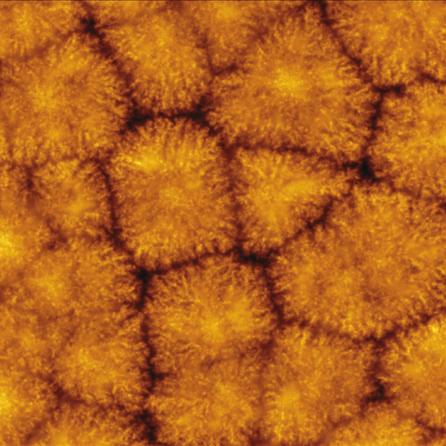
3 Unique NT-MDT SPM Features We are now proud to provide NT-MDT microscopes with the most advanced features, which include but not limited to the following: An expanded set of resonance oscillatory AFM modes: - Amplitude modulation with Phase Imaging The surface profile and probe phase changes are detected and mapped while the probe frequency and amplitude are fixed. - Amplitude modulation with Frequency Imaging The surface profile and probe frequency are detected and mapped while the probe amplitude and phase are fixed. - Frequency modulation The surface profile and probe amplitude are detected and mapped while the probe frequency shift and phase are fixed. F D A non-resonant oscillatory HybriD mode allowing direct and fast force detection for quantitative and high-resolution mapping of local sample Force Set-point deflection Stiffness Distance properties Baseline Adhesion t A suite of AFM-based electric modes that includes single and double pass techniques for measuring surface potential and capacitance gradients and unique thermoelectric imaging The exceptional low-noise and low thermal drift enclosure for stable imaging for a variety of applications 100 nm 51 min 100 nm Thermal Drift < 0.2 nm/min An open architecture software with multiple ways for controlling and monitoring the electronic signals during experiments starting with soft probe engagement Amplitude Soft Engagement Phase Probe Oscillator Ipr Bias Ext 5 GND GND Probe Sample Z-Approach Manual Computer simulation tools for theoretical evaluations of tip-sample interactions and their manifestation in most experimental AFM modes Low Force AM Images Tip Radius 150 pm Tip Radius 5 nm 3


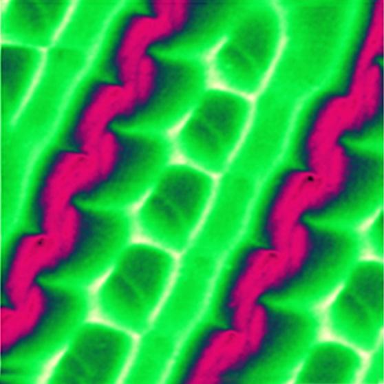
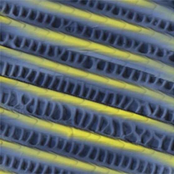
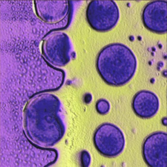
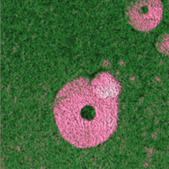
4 NT-MDT microscopes are equipped with closed loop scanners and are compatible with a wide range of accessories and a temperature stable enclosure providing exceptional noise protection. Nano Effective Solution for Education and Research SPM heads for novice and expert users Apprentice toolkit Flexible choice of probes Compact design and affordable cost NT-MDT Nano is a robust, small footprint SPM with a wide range of features: -- Educational head for STM & AFM intermittent contact mode by user made tips. -- Student toolkit to etch probes. -- Research head for most common AFM modes with commercially available tips. -- Routine imaging of nanoscale structures. Block copolymer Microporous membrane Celgard 300 nm C60H122 alkane on HOPG 2 mm 2 mm Nitrocellulose membrane NTEGRA Prima - Flexible Device for Routine and Advanced Applications Open architecture Tip/sample scanners Wide range of configurations/heads Broad temperature range NTEGRA Prima an Open-Architecture Modular Device for Advanced Research: -- Environmental and high-temperature measurements -- Specialized measurements with external magnetic fields -- Combination with Near-Field Optical Microscopy and Raman Spectroscopy -- Scanning in liquids with temperature control and flow-through capabilities -- Flexible scanning geometries and ranges Current 10 mm Polymer blend P3HT/PCBM Voltage (Seebeck) Map 10 mm Metallic alloy Bi/Sn 4


 40 mm Polymer blend PVDF/PVAC 40 mm Crystal of")


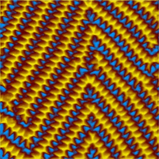
5 A powerful software package provides our users with flexibility to monitor and control a broad range of operational signals, starting with those used for soft probe engagement. NEXT Prime Automated Microscope Easy to use microscope with advanced capabilities Automated head exchange Automated laser/photodetector alignment Superscan and stitching capabilities NEXT is a unique system that provides researchers with outstanding performance and a wide range of capabilities. Specifically, it removes gap between optics and SPM by offering the users surface imaging from mm range down to the atomic scale. The exceptional functioning and automation of the alignment routines of this microscope make it the best candidate for high throughput studies in multi-user environments. Surface Potential 3 mm F14H20 fluoroalkane on HOPG (3D) 40 mm Polymer blend PVDF/PVAC 40 mm Crystal of C242H486 Etched Si Thermal Cabinet for NT-MDT Microscopes Unique solution for high-performance microscope environment Exceptional temperature stability Low-thermal drift medium Excellent acoustic and vibrational isolation This new fan-free enclosure provides NT-MDT microscopes the capability to operate at conditions of extraordinary temperature stability within 5 millidegree C. This guarantees the exceptionally low thermal drift of less than 0.2 nm/min. The cabinet also protects the positioned microscope from external acoustic and vibrational noises with passive and active means of damping. Time Plot of Temperatures of Sample Location and Room 0 C 31 sample location C nm nm Mica room MoSe min
 Tip Enhanced Raman")


 and smart probes (f) The open-design of NTEGRA Spectra")


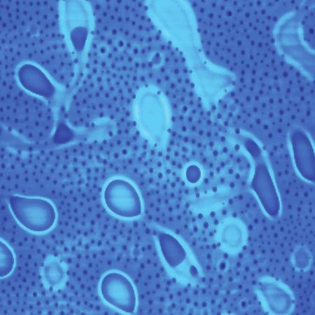
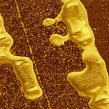
6 NTEGRA Spectra Enables AFM/Optics Synergy Co-localized AFM and optical measurements Near-field Optical Microscopy (SNOM/NSOM) Tip Enhanced Raman Scattering (TERS) With NT-MDT, Thermo Scientific, Renishaw and other spectrometers Focus track for optical measurements NTEGRA Spectra is an integrated solution for simultaneous AFM and Confocal Raman, Fluorescence, SNOM, TERS measurements. The instrument supports multiple AFM/Optics geometries enabling studies both in air and liquid. Comprehensive characterization of materials is achieved in combined mapping of chemically specific Raman bands and local mechanical and electrical properties. Raman mapping with nanometer resolution can be obtained by means of TERS. Similar resolution can be achieved for studies of plasmonic materials. AFM Raman, PVAC Raman, PS Counts 3000 PVAC - red PS - blue /cm Polymer blend PVAC/PS AFM/Optics Configurations for Illumination/Collection a d b e D-Band, D-Band, TERS TERS Map Map c f Inverted (b) Full transmission ( 4-Pi ) (c) Side-Illumination (d) SNOM: Optical fibers (e) and smart probes (f) The open-design of NTEGRA Spectra facilitates a broad spectrum of AFM/Optics applications for characterization of local chemical content, dielectric and plasmonic features in complex samples of various origins. They include polymers, carbon-based compounds, bio-materials, semiconductors etc. Spatial resolution of such measurements has approached the nanometer scale. AFM Overlayer of Raman Maps of CdS (green) and PANI (red) Graphene oxide Upright (a) CdS & polymer nanowires 6 SNOM, Whispering gallery modes 3 mm Semiconductor microdisc

 enabling measurements")


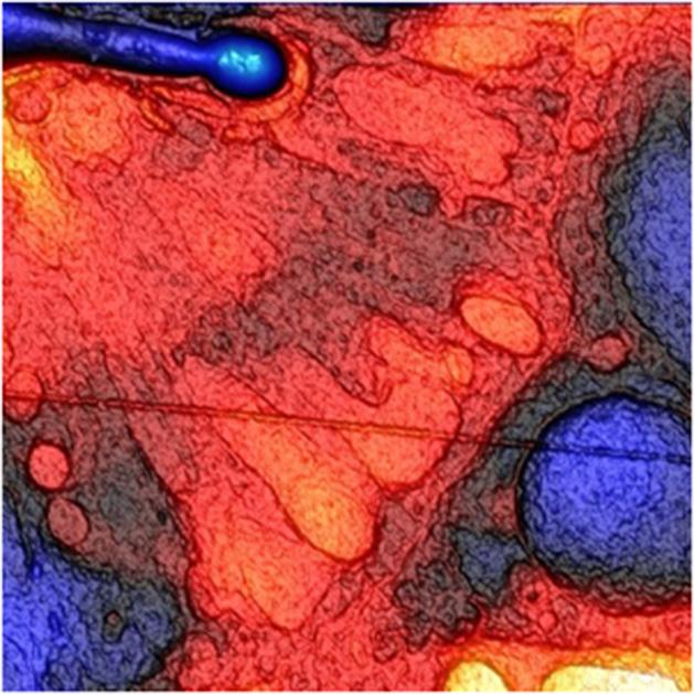
7 PX Controller the Core for High-Quality & Advanced SPM Built-in 5 lock-in amplifiers Detection channel up to 5 MHz Modular design Support all NT-MDT microscopes Our powerful PX digital controller incorporates a low-noise high voltage generator (< 1 mv/600 V), five lock-in amplifiers and sensitive detection electronics (up to 5 MHz) enabling measurements with negligible deflection noise (~25 fm/ Hz). The latter helps to make imaging in the atomic-scale as the routine procedure. The controller features provide a microscope user with a large spectrum of imaging and in single- and multi-frequency operations, which tremendously expand the research capabilities for visualization of surface structures and local quantitative studies of materials properties down to the nanoscale. Surface Potential dc/dz 1w dc/dv 2w 3w F14H20 fluoroalkanes on HOPG Hybrid Controller the True Gateway to New SPM Generation Fast signal detection and FPGA processing PLL and multiple digital broadband lock-in amplifiers Full synergy with Px controller Recently, NT-MDT microscopes were enhanced by the new Hybrid controller, which expands their instrumental and application capabilities by employing a high-speed (20 MHz) data acquisition and fast real-time data processing with FPGA at 80 MHz. New modes and applications are emerging with quantitative nanomechanical analysis in Hybrid mode being already routinely applied for elastic modulus mapping with 10-nm resolution. The expanded set of the oscillatory modes and other newly developed features (e.g. thermoelectric measurements) make the NT-MDT user the most powerful researcher compared to the practitioners of other SPM devices. Current Elastic Modulus t igh He m 6m 3.5 mm stic Ela 3.5 mm Carbon nanotubes on Si Polymer blend PVDF/sPS 7 s ulu d Mo Blockcopolymer PS/PMMA


8 NT-MDT America Inc S Kyrene Rd, # , Tempe, AZ info@ntmdt-america.com NT-MDT Head Office Building 100, Zelenograd, Moscow, Russia (499) spm@ntmdt.ru
Characterization of Materials with a Combined AFM/Raman Microscope
 Characterization of Materials with a Combined AFM/Raman Microscope Marko Surtchev 1, Sergei Magonov 1 and Mark Wall 2 1 NT-MDT America, Tempe, AZ U.S.A. 2 Thermo Fisher Scientific, Madison, WI, U.S.A.
Hysitron TI 980 TriboIndenter. Innovation with Integrity. Tribology and Mechanical Testing
 Hysitron TI 980 TriboIndenter World s Most Advanced Nanomechanical and Nanotribological Testing Innovation with Integrity Tribology and Mechanical Testing Hysitron TI 980 TriboIndenter Accelerate Nanomechanical
Magnetic Force Microscopy: nanoscale magnetic imaging and lithography
 NTEGRA Aura Magnetic Force Microscopy: nanoscale magnetic imaging and lithography The principle of Magnetic Force Microscopy (MFM) is based on the detection of the interaction between the sample and a
AFM-Raman Characterization of Pharmaceutical Tablets
 AFM-Raman Characterization of Pharmaceutical Tablets Compound Distribution Studies in Pharmaceutical Tablets by Integrated AFM-Raman Instrument 1,2 1 Sergey Shashkov and Pavel Dorozhkin, 1 NT-MDT Co.,
PeakForce Tapping and ScanAsyst An introduction to the technique featuring Bruker s Dimension Edge. Bede Pittenger, Ph.D.
 PeakForce Tapping and ScanAsyst An introduction to the technique featuring Bruker s Dimension Edge Bede Pittenger, Ph.D. Dimension Edge with ScanAsyst: High performance AFM breaking down cost and productivity
Acoustic and Vibration Isolation for Asylum Research AFMs
 Vibration Enclosures and Tables Acoustic and Vibration Isolation for Asylum Research AFMs DATA SHEET 01 Isolation from the lab environment plays an important role in image and measurement quality. Our
OSU MATERIALS RESEARCH SEED GRANT PROGRAM AWARDS
 2011-2012 OSU MATERIALS RESEARCH SEED GRANT PROGRAM AWARDS This Winter, the new OSU Materials Research Seed Grant Program was established as an enhanced seed program unifying the primary internal research
Dynamic Nanoindentation Characterization: nanodma III. Ude Hangen, Ph.D
 Dynamic Nanoindentation Characterization: nanodma III Ude Hangen, Ph.D. 2017-11-02 Displacement 11/02/2017 Bruker Confidential 2 nm mm mm Outline Elastic-Plastic vs. Viscoelastic Materials Response nanodma
Nanoindentation, Scratch and nanodma : Innovations for Atomic Force Microscopes. Ryan Stromberg
 Nanoindentation, Scratch and nanodma : Innovations for Atomic Force Microscopes Ryan Stromberg 09-07-2017 2 Outline Hysitron TriboScope Technology Mechanical Testing Indenter Stylus vs. AFM Cantilever
XPM: High Speed Nanoindentation and Mechanical Property Mapping. Eric Hintsala, Ph.D
 XPM: High Speed Nanoindentation and Mechanical Property Mapping Eric Hintsala, Ph.D. 2017-10-05 2 Table of Contents 1. Introduction: Brief overview of nanoindentation and nanomechanical property mapping
MultiMode 8 Upgrade. Benefits of Upgrading to the High-Performance AFM Benchmark
 MultiMode 8 Upgrade Benefits of Upgrading to the High-Performance AFM Benchmark What you will learn How much Multimode evolved: Easy to use Even higher lateral resolution Even more productive / faster
Full Nanomechanical Characterization of Ultra-Thin Films
 APPLICATION NOTE By: Jeffrey Schirer and Julia Nowak, Ph.D. Hysitron, Inc. Eiji Kusano and Mune-aki Sakamoto Department of Chemistry, Kanazawa Institute of Technology, Japan Full Nanomechanical Characterization
CREOL, The College of Optics & Photonics, University of Central Florida
 Metal Substrate Induced Control of Ag Nanoparticle Plasmon Resonances for Tunable SERS Substrates Pieter G. Kik 1, Amitabh Ghoshal 1, Manuel Marquez 2 and Min Hu 1 1 CREOL, The College of Optics and Photonics,
MAKE NO MISTAKE, IT S UV THAT EVERYONE CAN USE. LAMBDA 265 / 365 / 465 UV/Vis Solutions
 LAMBDA 265 / 365 / 465 UV/Vis Solutions MAKE NO MISTAKE, IT S UV THAT EVERYONE CAN USE 2 PUTTING OUR FOCUS ON THE NEEDS OF INDUSTRY AND ACADEMIA Based on our long history of UV/Vis leadership, our LAMBDA
FY06 ACCOMPLISHMENTS. Nanoelectronics Manufacture, Inspection, and Repair using Thermal Dip Pen Nanolithography
 FY06 ACCOMPLISHMENTS Nanoelectronics Manufacture, Inspection, and Repair using Thermal Dip Pen Nanolithography William P. King Georiga Institute of Technology FY06 was the second year of this grant, and
Nanomechanoelectrical characterization applications in fuel cells and organic photovoltaics
 Nanomechanoelectrical characterization applications in fuel cells and organic photovoltaics This article describes two nanoindentation based techniques, and demonstrates their utilities in fuel cells and
Supporting Information to Carbon Nanodots Towards a Comprehensive Understanding of their Photoluminescence
 Supporting Information to Carbon Nanodots Towards a Comprehensive Understanding of their Photoluminescence Volker Strauss, a, Johannes T. Margraf, a,b, Christian Dolle, c Benjamin Butz, c Thomas J. Nacken,
Satoshi Kawata. Near-Field Optic s and Surface Plasmon Polaritons
 Satoshi Kawata Near-Field Optic s and Surface Plasmon Polaritons Near-Field Optics and the Surface Plasmon Polariton Dieter W. Pohl 1 1. Introduction 1 2. Back to the Roots 1 2.1. Rayleigh and Mie Scattering
Park Systems Leading innovation in emerging nanoscale microscopy and metrology technology
 Park Systems Leading innovation in emerging nanoscale microscopy and metrology technology www.parkafm.com Park Systems Enabling Nanoscale Advances Table of Contents 4 Park Systems at a glance 5 We are
3D Laser Lithography in Biotechnology and Medical Technology
 3D Laser Lithography in Biotechnology and Medical Technology High-Precision, Piezo-Based Nanopositioning Systems Advance Technology Page 1 of 6 Laser technology makes it possible to create even very complex
INSTRUMENTAL TECHNIQUES FOR PARTICLE SIZE DETERMINATION
 CHAPTER V INSTRUMENTAL TECHNIQUES FOR PARTICLE SIZE DETERMINATION 5.1 INTRODUCTION Particle size determination is very essential and important while working with nanomaterials. There are a few good experimental
Keysight T150 UTM. Universal Testing Machine. Data Sheet
 Keysight T150 UTM Universal Testing Machine Data Sheet Overview The Keysight Technologies, Inc. T150 UTM is a universal testing machine that offers researchers a superior means of nanomechanical characterization.
nano-ta TM : Nano Thermal Analysis
 nano-ta TM : Nano Thermal Analysis Application Note #10 Correlation between nanoscale and bulk Thermal Analysis Authors: Dr. Greg Meyers and Dr. Andrew Pastzor Dow Chemical Introduction Thermal methods
The Unlimited World of Applications for Nano & Photonics. Benno Oderkerk CEO Avantes BV, Apeldoorn, The Netherlands
 The Unlimited World of Applications for Nano & Photonics Benno Oderkerk CEO Avantes BV, Apeldoorn, The Netherlands Contents Avantes Introduction Photonics NL Introduction TKI Chemie Nanotechnology and
High-Resolution, Electrohydrodynamic Inkjet Printing of Stretchable, Metal Oxide Semiconductor Transistors with High Performances
 Electronic Supplementary Material (ESI) for Nanoscale. This journal is The Royal Society of Chemistry 2016 ` Electronic Supplementary Information High-Resolution, Electrohydrodynamic Inkjet Printing of
Keysight Technologies Laser Heated Tip and High Temperature Stage for G200 Nano Indenter. Data Sheet
 Keysight Technologies Laser Heated Tip and High Temperature Stage for G200 Nano Indenter Data Sheet Overview The Nano Indenter G200 from Keysight Technologies, Inc. is the world s most flexible, and user-friendly
Keysight Technologies Imaging with Self-Sensing Cantilever on Keysight 5500/5600LS Atomic Force Microscopes. Application Note
 Keysight Technologies Imaging with Self-Sensing Cantilever on Keysight 5500/5600LS Atomic Force Microscopes Application Note Introduction Atomic force microscopy (AFM), a key member of the scanning probe
DeltaPro. DeltaFlex FORENSICS PARTICLE CHARACTERIZATION ELEMENTAL ANALYSIS FLUORESCENCE GRATINGS & OEM SPECTROMETERS OPTICAL COMPONENTS RAMAN
 DeltaFlex DeltaPro ELEMENTAL ANALYSIS FLUORESCENCE GRATINGS & OEM SPECTROMETERS OPTICAL COMPONENTS FORENSICS PARTICLE CHARACTERIZATION RAMAN SPECTROSCOPIC ELLIPSOMETRY SPR IMAGING Why measure fluorescence
Friction, Scratching/Wear, Indentation, and Lubrication Using Scanning Probe Microscopy
 19 Friction, Scratching/Wear, Indentation, and Lubrication Using Scanning Probe Microscopy Bharat Bhushan The Ohio State University 19.1 Introduction 19.2 Description of AFM/FFM and Various Measurement
NIR Checkmaster Near-infrared spectroscopy On-line analysis of active ingredients during tablet production
 NIR Checkmaster Near-infrared spectroscopy On-line analysis of active ingredients during tablet production Slash release times with NIR Innovative features Fully automatic assay of tablet weight, hardness,
NanoSystemsEngineering: NanoNose Final Status, March 2011
 1 NanoSystemsEngineering: NanoNose Final Status, March 2011 The Nanonose project is based on four research projects (VCSELs, 3D nanolithography, coatings and system integration). Below, the major achievements
Transmission Kikuchi Diffraction in the Scanning Electron Microscope
 Transmission Kikuchi Diffraction in the Scanning Electron Microscope Robert Keller, Roy Geiss, Katherine Rice National Institute of Standards and Technology Nanoscale Reliability Group Boulder, Colorado
Status of the DESY NanoLab Project
 Status of the DESY NanoLab Project Ralf Röhlsberger DESY Wissenschaftlicher Ausschuss DESY 7 June 2011 Mission of the DESY NanoLab To accomodate the growing need for structural probes on the nanoscale,
Morphology of Thin Aluminum Film Grown by DC Magnetron Sputtering onto SiO 2 on Si(100) Substrate
 Substrate") Morphology of Thin Aluminum Film Grown by DC Magnetron Sputtering onto SiO 2 on Si(1) Substrate Fan Wu Microelectronics Center, Medtronic Inc., Tempe, AZ 85261 James E. Morris Department of Electrical
Morphology of Thin Aluminum Film Grown by DC Magnetron Sputtering onto SiO 2 on Si(1) Substrate Fan Wu Microelectronics Center, Medtronic Inc., Tempe, AZ 85261 James E. Morris Department of Electrical
YIELD & TENSILE STRENGTH OF STEEL & ALUMINIUM USING MICROINDENTATION
 YIELD & TENSILE STRENGTH OF STEEL & ALUMINIUM USING MICROINDENTATION Prepared by Duanjie Li, PhD & Pierre Leroux 6 Morgan, Ste156, Irvine CA 9618 P: 949.461.99 F: 949.461.93 nanovea.com Today's standard
The Raman effect, discovered in 1928 by C.V. Raman in his
 Refined Raman Spectroscopy Bringing New Insight into INDUSTRIAL PROCESSES Sophie Morel and Fran Adar Fiber probes and ease of use make Raman spectroscopy systems attractive for monitoring process control
Confocal Microscopy Analyzes Cells
 Choosing Filters for Fluorescence A Laurin Publication Photonic Solutions for Biotechnology and Medicine November 2002 Confocal Microscopy Analyzes Cells Reprinted from the November 2002 issue of Biophotonics
Fabrication and STM Nanostructuring of tetrahedral amorphous Carbon. Teja Roch
 Fabrication and STM Nanostructuring of tetrahedral amorphous Carbon Teja Roch Fabrication and STM Nanostructuring of tetrahedral amorphous Carbon (ta-c) Content: Who are we? What are we doing? Why are
Low temperature deposition of thin passivation layers by plasma ALD
 1 Low temperature deposition of thin passivation layers by plasma ALD Bernd Gruska, SENTECH Instruments GmbH, Germany 1. SENTECH in brief 2. Low temperature deposition processes 3. SENTECH SI ALD LL System
DSC differential scanning calorimeter (DSC)
") THERMAL ANALYZERS DSC- 2200 differential scanning calorimeter (DSC) Product introduction: DSC is designed to determine the inner heat transition relating to temperature and heat flow, it is widely used
THERMAL ANALYZERS DSC- 2200 differential scanning calorimeter (DSC) Product introduction: DSC is designed to determine the inner heat transition relating to temperature and heat flow, it is widely used
Featuring Analyst software under Windows NT for enhanced performance and ease of use. API 150EX. LC/MS System
 Featuring Analyst software under Windows NT for enhanced performance and ease of use. API 15EX LC/MS System compact, rugged, The API 15EX LC/MS System is the most rugged and reliable single quadrupole
Digital resolution enhancement in surface plasmon microscopy
 Digital resolution enhancement in surface plasmon microscopy I.I. Smolyaninov 1) *, J. Elliott 2), G. Wurtz 2), A.V. Zayats 2), C.C. Davis 1) 1) Department of Electrical and Computer Engineering, University
Evaluation of Interphase Properties in Fiber Reinforced Polymer Composite Using Contact Resonance Force Microscopy
 Evaluation of Interphase Properties in Fiber Reinforced Polymer Composite Using Contact Resonance Force Microscopy Sandeep S. Nair, Siqun Wang Tennessee Forest Products Center University of Tennessee Knoxville,
Plasmonics: Application-oriented fabrication. Part 1. Introduction
 Plasmonics: Application-oriented fabrication Part 1. Introduction Victor Ovchinnikov Department of Aalto Nanofab Aalto University Espoo, Finland Alvar Aalto was a famous Finnish architect and designer
Enhanced Response from Engineered Nano Treated Peizofilm
 Enhanced Response from Engineered Nano Treated Peizofilm By Sai Narayan Sundar Advisor Dr J.P Sharma Dept. of Mechanical Engineering University of Mississippi i: flow of current due to piezo deformation
EDGE CHIPPING RESISTANCE USING MACROINDENTATION TESTING
 EDGE CHIPPING RESISTANCE USING MACROINDENTATION TESTING Prepared by Ali Mansouri 6 Morgan, Ste156, Irvine CA 92618 P: 949.461.9292 F: 949.461.9232 nanovea.com Today's standard for tomorrow's materials.
Application of the interference method of studying the surface for quality control and internal structure of the luminescent crystals and
 Application of the interference method of studying the surface for quality control and internal structure of the luminescent crystals and microelectronic products. First name: Byller A.I. Kyleshov V.K.
CB x 33 x 70 cm
 MECHANICAL TESTERS The Mechanical Tester has been designed with leading edge technologies in order to give the highest accuracy and repeatability on the widest range of measurements. This focus on quality
ADHESIVE CURE MONITORING WITH ACOUSTIC METHOD
 ADHESIVE CURE MONITORING WITH ACOUSTIC METHOD I. Severina, E. Maeva Industrial Research Chair In Applied Solid State Physics and Material Characterization, University of Windsor, Windsor, Canada Abstract:
Syringe Pumps. Please contact us for help in selecting the best pump for your application and a free quote.
 Syringe Pumps Microfluidic Pumps! We are proud to offer select Harvard Apparatus syringe pumps for use with SynVivo biochips. These high quality pumps have been extensively tested and offer a feature rich
Greenhouse Gas Measurement Technology
 Greenhouse Gas Measurement Technology Michael Corvese Thermo Fisher Scientific March 25, 2010 Agenda Introduction GHG Regulatory Current Methods Infrared Spectroscopy GC FID Emerging Methods Laser-Based
Fluke Oscilloscope Calibration Solutions. Helping you measure up to the highest standards
 Fluke Oscilloscope Calibration Solutions Helping you measure up to the highest standards Fluke offers more ways to meet your oscilloscope calibration needs If your organization is like most, you are competing
The AFM Probe - Fundamentals, Selection, and Applications
 The AFM Probe - Fundamentals, Selection, and Applications Introduction Appropriate selection of AFM probe can be one of the most important decisions to be made towards a successful AFM experiment As there
Phase Transitions Module γ-2: VSM study of Curie Temperatures 1 Instructor: Silvija Gradečak
 3.014 Materials Laboratory November 13 th 18 th, 2006 Lab week 3 Phase Transitions Module γ-2: VSM study of Curie Temperatures 1 Instructor: Silvija Gradečak Objectives: a) Understand magnetic and thermal
Proudly serving laboratories worldwide since 1979 CALL for Refurbished & Certified Lab Equipment QTRAP 5500
 www.ietltd.com Proudly serving laboratories worldwide since 1979 CALL +847.913.0777 for Refurbished & Certified Lab Equipment QTRAP 5500 Powerful synergy results when the world s most sensitive triple
Application of ultra-thin aluminum oxide etch mask made by atomic layer deposition technique
 IOP Publishing Journal of Physics: Conference Series 61 (2007) 369 373 doi:10.1088/1742-6596/61/1/074 International Conference on Nanoscience and Technology (ICN&T 2006) Application of ultra-thin aluminum
nanodsf 2bind: Your service provider for biophysical characterization of proteins Precisely revealing protein folding and stability
 nanodsf Precisely revealing protein folding and stability 2bind: Your service provider for biophysical characterization of proteins This booklet was written and designed by 2bind 08 2015 Any reproduction
State of the art quality of a GeOx interfacial passivation layer formed on Ge(001)
") APPLICATION NOTE State of the art quality of a Ox interfacial passivation layer formed on (001) Summary A number of research efforts have been made to realize Metal-Oxide-Semiconductor Field Effect Transistors
APPLICATION NOTE State of the art quality of a Ox interfacial passivation layer formed on (001) Summary A number of research efforts have been made to realize Metal-Oxide-Semiconductor Field Effect Transistors
R Sensor resistance (Ω) ρ Specific resistivity of bulk Silicon (Ω cm) d Diameter of measuring point (cm)
 ρ Specific resistivity of bulk Silicon (Ω cm) d Diameter of measuring point (cm)") 4 Silicon Temperature Sensors 4.1 Introduction The KTY temperature sensor developed by Infineon Technologies is based on the principle of the Spreading Resistance. The expression Spreading Resistance derives
4 Silicon Temperature Sensors 4.1 Introduction The KTY temperature sensor developed by Infineon Technologies is based on the principle of the Spreading Resistance. The expression Spreading Resistance derives
PRECISION OPTICAL FILTERS BY EOSS - ENHANCED OPTICAL SPUTTERING SYSTEM. Fraunhofer
 PRECISION OPTICAL FILTERS BY EOSS - ENHANCED OPTICAL SPUTTERING SYSTEM EOSS ENHANCED OPTICAL SPUTTERING SYSTEM Fraunhofer IST, Braunschweig Contact: Dr. M. Vergöhl +49 531 2155 640 EOSS Coating System
Microscopic Damage of Tungsten and Molybdenum Exposed to Low-Energy Helium Ions
 Plasma Science and Technology, Vol.17, No.4, Apr. 2015 Microscopic Damage of Tungsten and Molybdenum Exposed to Low-Energy Helium Ions FAN Hongyu ( ) 1,3, YANG Qi ( ) 1,3,LIXin( ) 1,3, NI Weiyuan ( ) 1,3,NIUJinhai(
Confocal Microscopy of Electronic Devices. James Saczuk. Consumer Optical Electronics EE594 02/22/2000
 Confocal Microscopy of Electronic Devices James Saczuk Consumer Optical Electronics EE594 02/22/2000 Introduction! Review of confocal principles! Why is CM used to examine electronics?! Several methods
Piezoelectric All-Rounder
 Piezoelectric All-Rounder Sensor, Actuator or Both? PI Ceramic GmbH, Lindenstraße, 07589 Lederhose, Germany Page 1 of 5 The Piezo Effect By the end of the 19th century Jacques und Pierre Curie had already
EV Group 300mm Wafer Bonding Technology July 16, 2008
 EV Group 300mm Wafer Bonding Technology July 16, 2008 EV Group in a Nutshell st Our philosophy Our mission in serving next generation application in semiconductor technology Equipment supplier for the
CHAPTER 3 IMPROVEMENT OF DYNAMIC CHARACTERISTICS OF CUTTING TOOL SYSTEM USING VISCOELASTIC DAMPER
 44 CHAPTER 3 IMPROVEMENT OF DYNAMIC CHARACTERISTICS OF CUTTING TOOL SYSTEM USING VISCOELASTIC DAMPER This chapter introduces a novel design for turning tool holder assembly with enhanced damping capability.
Repetition: Adhesion Mechanisms
 Repetition: Adhesion Mechanisms a) Mechanical interlocking b) Monolayer/monolayer c) Chemical bonding d) Diffusion e) Psedo diffusion due to augmented energy input (hyperthermal particles) Repetition:
DESIGNING WITH WAVY COMPOSITES
 DESIGNING WITH WAVY COMPOSITES Dr. William F. Pratt and Matthew S. Allen Patterned Fiber Composites, Inc. Lindon, UT 8442 Dr. C. Greg Jensen Brigham Young University Provo, UT 8462 ABSTRACT Wavy composite
Nanobiotechnology. Place: IOP 1 st Meeting Room Time: 9:30-12:00. Reference: Review Papers. Grade: 50% midterm, 50% final.
 Nanobiotechnology Place: IOP 1 st Meeting Room Time: 9:30-12:00 Reference: Review Papers Grade: 50% midterm, 50% final Midterm: 5/15 History Atom Earth, Air, Water Fire SEM: 20-40 nm Silver 66.2% Gold
SUPPLEMENTARY INFORMATION
 In the format provided by the authors and unedited. ARTICLE NUMBER: 16178 DOI: 10.1038/NENERGY.2016.178 Enhanced Stability and Efficiency in Hole-Transport Layer Free CsSnI3 Perovskite Photovoltaics Supplementary
Application Note #1007 All-Inclusive Scratch Testing of Coatings and Thin Films Using Bruker's Universal Test System
 Scratch with ECR Scratch with E UMT TriboLab pplication Note #1007 ll-inclusive Scratch Testing of Coatings and Thin Films Using ruker's Universal Test System Coatings and thin films are being used increasingly
Self-Assembled Nanocrystals Through Change in. Nanocrystallinity
 Supporting informations Modulating Physical Properties of Isolated and Self-Assembled Nanocrystals Through Change in Nanocrystallinity Nicolas Goubet,, Cong Yan,, Dario Polli, Hervé Portalès,, Imad Arfaoui,,
NovoCyte Flow Cytometer
 NovoCyte Flow Cytometer The Flow Cytometer for Everyone 2 Experience the NovoCyte Advantage Focus on advancing your research. Let the flow cytometer do the rest. NovoCyte Flow Cytometer High Performance
Sapphire SF: Low-Noise Ultra-Narrow Bandwidth Performance Delivers Superior Raman Spectroscopy Results
 White Paper Sapphire SF: Low-Noise Ultra-Narrow Bandwidth Performance Delivers Superior Raman Spectroscopy Results Based on field-proven optically pumped semiconductor laser (OPSL) technology, recent data
Silicon Nitride Probes
 1 Silicon Nitride Probes NEW We are happy to announce the introduction of MikroMasch Silicon Nitride XNC12 series* of AFM. These are intended for contact mode measurements on biological and other soft
Surface Plasmon Resonance Systems
 Innovative precision instruments for over a century Surface Plasmon Resonance Systems Label-free Molecular Interaction Analysis ReichertSPR Answers: Is there an interaction? How fast? How strong? How long?
Transmission Electron Microscopy (TEM) Prof.Dr.Figen KAYA
 Prof.Dr.Figen KAYA") Transmission Electron Microscopy (TEM) Prof.Dr.Figen KAYA Transmission Electron Microscope A transmission electron microscope, similar to a transmission light microscope, has the following components along
Transmission Electron Microscopy (TEM) Prof.Dr.Figen KAYA Transmission Electron Microscope A transmission electron microscope, similar to a transmission light microscope, has the following components along
Supporting Information
 Copyright WILEY-VCH Verlag GmbH & Co. KGaA, 69469 Weinheim, Germany, 2013. Supporting Information for Adv. Energy Mater., DOI: 10.1002/aenm.201300184 Screen-Printable Thin Film Supercapacitor Device Utilizing
Imaging of in Vitro Collagen Fibers by Atomic Force Microscopy
 Imaging of in Vitro Collagen Fibers by Atomic Force Microscopy Undergraduate Researcher Isabel Nocedal, Northwestern University Faculty Mentors Horacio Espinosa Department of Mechanical Engineering, Northwestern
Vibration Control SCHWINGMETALL. The Original Rubber-To-Metal Bonding from ContiTech
 Vibration Control SCHWINGMETALL The Original Rubber-To-Metal Bonding from ContiTech ContiTech Vibration Control Innovator and Development Partner ContiTech is an innovator and development partner for vibration-damping
350 C for 8 hours in argon atmosphere. Supplementary Figures. Supplementary Figure 1 High-temperature annealing of BP flakes on SiO 2.
 Supplementary Figures Supplementary Figure 1 High-temperature annealing of BP flakes on SiO 2. (a-d) The optical images of three BP flakes on a SiO 2 substrate before (a,b) and after annealing (c,d) at
Amorphous Oxide Transistor Electrokinetic Reflective Display on Flexible Glass
 Amorphous Oxide Transistor Electrokinetic Reflective Display on Flexible Glass Devin A. Mourey, Randy L. Hoffman, Sean M. Garner *, Arliena Holm, Brad Benson, Gregg Combs, James E. Abbott, Xinghua Li*,
Thin Film Characterisation Methods
 Thin Film Characterisation Methods Technologies Hardness /Adhesion Nanoindentation Plasma Diagnostics and Particle Flux Analysis Raman Spectroscopy Film Thickness Magnetometer (VSM) and High Frequency
PinAAcle 500. Flame Atomic Absorption Spectrometer
 PinAAcle 500 Flame Atomic Absorption Spectrometer RELIABILITY SENSITIVITY AFFORDABILITY Engineered to deliver an uncompromising level of performance at an unbeatable price, the PinAAcle 500 puts the industry
Universität Hamburg, Hamburg, Germany. Universität Hamburg, Hamburg, Germany
 Sample Preparation, Micromagnetic Simulations, Circular-Rotational Currents, Parasitic Oersted Fields and Clover Samples (Magnetic Antivortex-Core Reversal by Circular-Rotational Spin Currents) Thomas
Thermal Annealing Effects on the Thermoelectric and Optical Properties of SiO 2 /SiO 2 +Au Multilayer Thin Films
 American Journal of Materials Science 2015, 5(3A): 31-35 DOI: 10.5923/s.materials.201502.05 Thermal Annealing Effects on the Thermoelectric and Optical Properties of SiO 2 /SiO 2 +Au Multilayer Thin Films
Characterization of Cellulose Nanocrystal Surfaces by SPM
 Characterization of Cellulose Nanocrystal Surfaces by SPM R.R, Lahiji 1,2, R. Reifenberger 1,2, A. Raman 1,3, Alan Rudie 4, and R. J. Moon 1,4,5 1 Birck Nanotechnology Center, Purdue University 2 Department
Thin, Smooth Diamond for Breakthrough Solutions
 Thin. Smooth. Diamond. Thin, Smooth Diamond for Breakthrough Solutions Advanced Diamond Technologies (ADT) harnesses the extreme properties of nature s perfect material by turning natural gas into diamond
Thermal Analysis Excellence
 Thermal Analysis Excellence DMA/SDTA861 e STAR e System Innovative Technology Versatile Modularity Swiss Quality Dynamic Mechanical Analysis Sets New Standards DMA/SDTA861 e Precise Measurement Technology
12.0 Materials for Missile, Space, and Launch Systems
 12.0 Materials for Missile, Space, and Launch Systems 12.1 Introduction Affordability is the key criterion for assessing the value of a new technology and its potential incorporation into military applications.
X-ray Photoelectron Spectroscopy
 X-ray Photoelectron Spectroscopy X-ray photoelectron spectroscopy (XPS) is a non-destructive technique used to analyze the elemental compositions, chemical and electronic states of materials. XPS has a
Laser Synthesis of Metal Oxide Crystals with the Use of Carbon Nanotubes
 Open Journal of Composite Materials, 2013, 3, 16-20 http://dx.doi.org/10.4236/ojcm.2013.32a003 Published Online April 2013 (http://www.scirp.org/journal/ojcm) Laser Synthesis of Metal Oxide Crystals with
SORTEX B range. Optimising conventional sorting.
 range. Optimising conventional sorting. . Optimising conventional sorting. Changing the game - demonstrating a commitment to help processors get the most value from optical sorting, Bühler's high capacity
BioScope Catalyst Life Science Atomic Force Microscope
 BioScope Catalyst Life Science Atomic Force Microscope New Standard for AFM and Light Microscope Integration Uncompromised Performance from Both Techniques Increased Productivity and Ease of Use Simple,
Optimization of optical performances in submicron silicon-on-insulator rib and strip waveguides by H 2 thermal annealing
 I N S T I T U T D E R E C H E R C H E T E C H N O L O G I Q U E Optimization of optical performances in submicron silicon-on-insulator rib and strip waveguides by H thermal annealing Erwine Pargon 1, Cyril
An Advanced Reliability Improvement and Failure Analysis Approach to Thermal Stress Issues in IC Packages
 An Advanced Reliability Improvement and Failure Analysis Approach to Thermal Stress Issues in IC Packages Michael Hertl 1, Diane Weidmann 1, and Alex Ngai 2 1 Insidix, 24 rue du Drac, F-38180 Grenoble/Seyssins,
Superionic Solid State Stamping (S4)
") Superionic Solid State Stamping (S4) Lead Faculty Researcher: Placid Ferreira Department: Materials Science & Engineering Hsu et al, Nano Letters, 2007 1. Description: This dry, single step, electrochemical
Superionic Solid State Stamping (S4) Lead Faculty Researcher: Placid Ferreira Department: Materials Science & Engineering Hsu et al, Nano Letters, 2007 1. Description: This dry, single step, electrochemical
Plasmonic Probe With Circular Nano-Moat for far-field Free Nanofocusing
 Zhang and Wang Nanoscale Research Letters (2016) 11:421 DOI 10.1186/s11671-016-1619-y NANO EXPRESS Plasmonic Probe With Circular Nano-Moat for far-field Free Nanofocusing Mingqian Zhang 1* and Tianying
Biofluids Analysis: Human Serum with High Throughput NMR
 Biofluids Analysis: Human Serum with High Throughput NMR Analysis of biofluids can provide a detailed and specific view into pharmaceutically relevant processes and conditions; most importantly metabolism