Low temperature deposition of thin passivation layers by plasma ALD
|
|
|
- Mildred Cain
- 6 years ago
- Views:
Transcription
1 1 Low temperature deposition of thin passivation layers by plasma ALD Bernd Gruska, SENTECH Instruments GmbH, Germany 1. SENTECH in brief 2. Low temperature deposition processes 3. SENTECH SI ALD LL System 4. Properties of ALD Al 2 O 3 films 5. Summary

2 2 SENTECH in brief Private company founded in 1990 Located in Berlin, Germany New building since employees ISO 9001 certificated Business fields Thin Film Metrology Metrology for PV Plasma Process Technology Atomic Layer Deposition

3 3 SENTECH in brief Located in Berlin-Adlershof, Germany s largest science and technology park WISTA-MG


4 SENTECH in brief Application experts at SENTECH Processing of customer samples Device demonstrations User training Application fields: R & D Quality control Photovoltaic Low damage etching Low temperature deposition Nano patterning Nano films 3D deposition 4


5 5 Plasma Process Technology Plasma ALD Plasma deposition Cluster tool RIE, ICP-RIE PECVD, ICPECVD Cluster tools ALD / PEALD SENTECH laser end point monitor Endpoint monitor Plasma etching
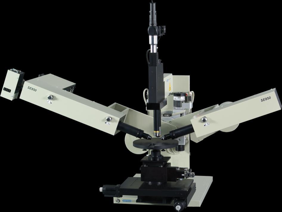


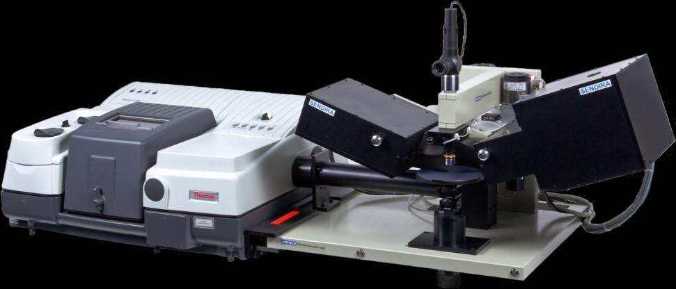

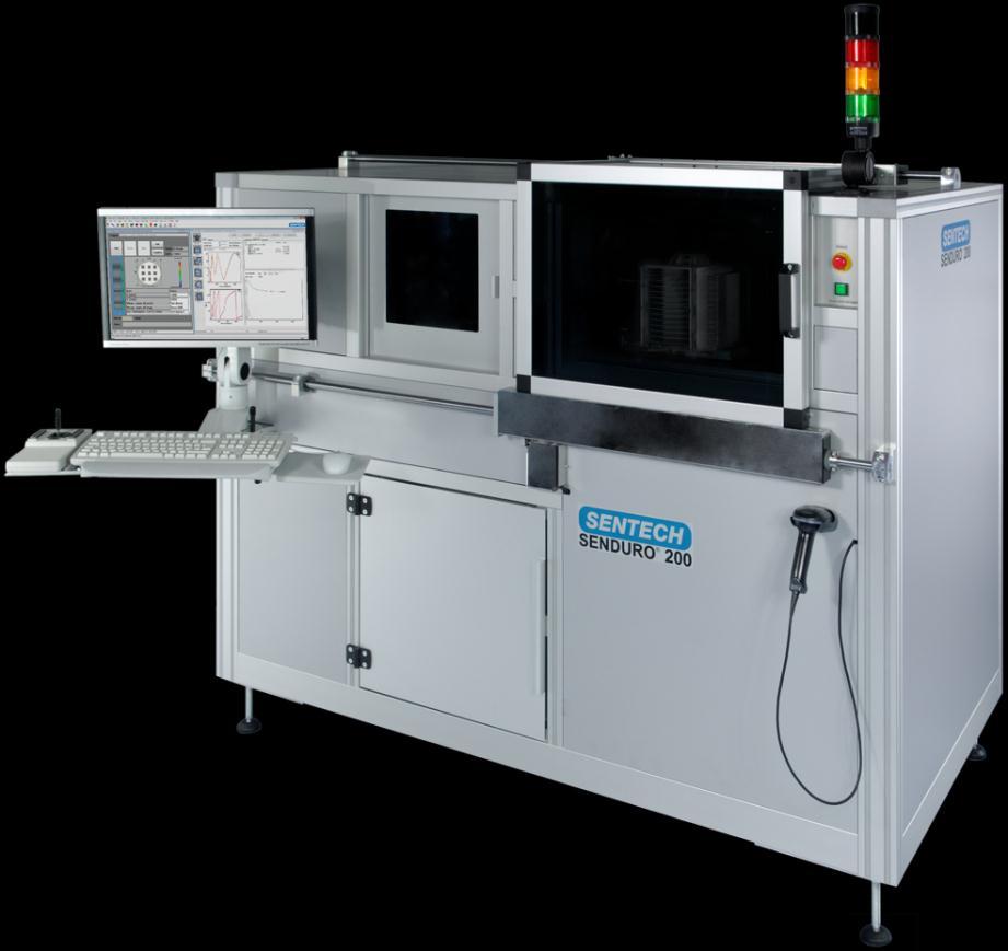
6 6 Spectroscopic ellipsometers SENresearch for R&D and quality control Wide spectral range Highly flexible SE 850 DUV SENDURO 200/300 SENDIRA
7 Low temperature deposition processes Applications of low temperature deposition processes Passivation of organic materials (OLEDs) (T D 80 C) Isolation of interconnects on small gap compound semiconductors (T D C) Passivation of pn-structures (mesas) of compound semiconductors (T D 200 C) 7
8 Low temperature deposition processes Deposition methods Inductively coupled plasma enhanced chemical deposition (ICPECVD) Plasma enhanced atomic layer deposition (PEALD) 8

9 Low temperature deposition processes ICPECVD SI 500 D ICP planar plasma source RT-400 C Gasses: SiH4, O2, NH3, N2, H2, CH4 Films :SiO2, SiNx, SiOxNy, a-si, SiC Growth rate: nm/min Conformality:~0.7:1 Low ion energy, <10 ev 9
10 Capacitance [F] compressiv - (10 8 Pa) - tensil Main properties of ICPECVD films T = 130 C, n = ICPECVD PECVD 0-1 Si-H Absorption /cm P ICP, flow NH 3 flow p ( Pa ) Deposition temperature / C f=1mhz QSCV HFCV and QSCV ICPJ6 2.2E E-10 2E E E E E E E E E Bias Voltage [V] MOS barrier ICPECVD: SiO x, T= 260 C n B = N ss = 0.2*10 11 cm -2 ev -1 E B = 8.6 MV/cm r = 1.1*10 18 Ohm cm 10
11 11 Low temperature deposition processes Atomic Layer Deposition Complete control of deposition process in a nanometer scale Conformal coatings into high aspect ratio structures Pin-hole and particle free depositions Low temperature deposition by plasma enhanced ALD PEALD removes water as precursor Wide range of chemistry for film deposition
 TMA chemisorption 2) Purging step 3) Water chemisorption 4)")

![solar cells [1] - Diffusion barriers in organic electronics [2] - Gate](/docs-images/73/68871963/images/12-3.jpg "dielectrics in transistors [3, 4] - Passivation layers in Li-Ion")
12 12 Atomic Layer Deposition of Al 2 O 3 ALD cycle using TMA and water vapor: 1) TMA chemisorption 2) Purging step 3) Water chemisorption 4) Purging step Applications: ALD Al 2 O 3 films have been investigated in different applications, such as: - Charge-recombination layers in solar cells [1] - Diffusion barriers in organic electronics [2] - Gate dielectrics in transistors [3, 4] - Passivation layers in Li-Ion batteries [5]
13 SENTECH SI ALD LL System Specifications Substrate size up to 8 Substrate temperature 400 (up to 600 C optional) Reactor wall temperature 150 C (optional 200 C) Precursor lines up to 4 separate inlets direct draw or bubble line 200 C heated heater jacket for container Gas lines up to 7 Plasma source true remote CCP source (option) In-situ diagnostic SENTECH ellipsometer QMS, QMC Options TMP with isolation valve Ozone line, Glove box Clusterable to other process modules 13

 - Manual and")
14 14 SENTECH SI ALD LL System Systeme software - User-friendly, based on SENTECH plasma system software - Special tool for operating ALD-pulses - Reliable remote field controller (RFC) - Manual and automatic operation
15 15 SENTECH SI ALD LL System In-situ analysis Optional available: - Ellipsometry (laser, spectroscopic) - Mass Spectrometer (QMS) - Quartz Crystal Microbalance (QCM) Applications: Growth Satturation Resistivity Reation mechanismus Chamber conditions Precursor behavior LE, SE, QMC LE, SE, QMC SE QMC, QMS QMS QMS
16 16 SENTECH SI ALD LL System In-situ analysis by laser ellipsometry 25 / / d = 0 nm calculated transients for n= measured transient / Al 2 O 3 thickness / nm thickness / nm growth start time / s / d = 40 nm d Al2O3 = nm n Al2O3 = 1.64 = 65 T = 200 C n=1.55 n=1.65 n= n=1.85 n= /

17 17 SENTECH SI ALD LL System Key features of SI PEALD LL Flexible system architecture A wide range of processes and applications Thermal and plasma enhanced processing Plasma source can be separated from the system True remote plasma source Substrate outside of the plasma generation region In-situ diagnostic capability SENTECH ellipsometers, QMS Rugged design and small footprint System can be connected to cluster tool L x W x H: 1800 x 680 x 1840 mm²
 Sigma 0,283nm Growth rate 0,8 Å/cycle")
18 18 Properties of ALD Al 2 O 3 films Thermal ALD on 8" Wafer, thickness and R.I uniformity Layer thickness Refractive index TMA + H 2 O: Layer thickness: 8" Wafer 49,9nm (± 1,2%) Sigma 0,283nm Growth rate 0,8 Å/cycle Substrate temperature 200 C n (@632,8 nm) 1,639 (± 0,15%) Cycle time 2 s

 Sigma 0,232nm Growth rate 1,1 Å/cycle")
19 19 Properties of ALD Al 2 O 3 films Plasma enhanced ALD on 8" Wafer, thickness and R.I. uniformity Layer thickness Refractive index TMA + O 2 -Plasma: Layer thickness: 8" Wafer 26,8nm (± 1,6%) Sigma 0,232nm Growth rate 1,1 Å/cycle Substrate temperature 200 C n (@632,8 nm) 1,642 (± 0,58%) Cycle time 10,5 s
20 20 Properties of ALD Al 2 O 3 films Linearity of growth - Al 2 O 3 film thickness shows linear dependence on the number of cycles in ALD and PEALD. - PEALD provides a higher growth rate of 1.2 Å/cycle compared to ALD. The growth rate in ALD amounts 0.8 Å/cycle. Process parameter ALD PEALD Substrate temperature ( C) Process pressure (Pa) Plasma power (W) Growth rate (Å/Cycle) Cycle time (s) 4 8
 Prepared samples were treated with O 2 -plasma to remove resist and examined with REM*. Very good conformality to 3D structures *) Thanks to Dr.")
21 21 Properties of ALD Al 2 O 3 films Conformality 18 nm ALD-Al 2 O 80 C 21 nm PEALD-Al 2 O 80 C 1) 3D resist structures were prepared on Si-Wafers* and coated with ALD and PEALD Al 2 O 3 at 80 C substrate temperature. 2) Prepared samples were treated with O 2 -plasma to remove resist and examined with REM*. Very good conformality to 3D structures *) Thanks to Dr. Hübner, IPHT-Jena, Germany, for preparing the 3D structures and doing the REM-measurement.
22 Depositionsrate [Å/cycle] Refractive index n 22 Properties of ALD Al 2 O 3 films Low temperature deposition of Al 2 O 3 by PEALD PEALD Al 2 O 3 PEALD Al 2 O ALD Al 2 O ALD Al 2 O Substrate temperature [ C] Substrate temperature [ C]
23 C/Al [a.u.] Absorption index 23 Properties of ALD Al 2 O 3 films Chemical information XPS Al-O 200 C IR spectroscopy IR ellipsometer SENDIRA C C Substrate temperature [ C] Impurities, methyl groups Wavenumber / cm -1


24 24 Summary - Outstanding features of SI PEALD-systems: Flexible system configuration for a wide range of processes and applications True remote plasma CCP source In-situ control by ellipsometry Rugged design and small footprint - Process results: Thermal and plasma enhanced deposition: very good uniformity Thermal and plasma enhanced deposition: very good conformality Incorporation of methyl groups at low temperature depositions Outlook Process optimization based on IR ellipsometry, in-situ laser ellipsometry

25 25 Thank you for your attention Visit us at booth of Energo Avangard SENTECH Instruments GmbH (Berlin)
ALD systems and SENTECH Instruments GmbH
 ALD systems and processes @ SENTECH Instruments GmbH H. Gargouri, F. Naumann, R. Rudolph and M. Arens SENTECH Instruments GmbH, Berlin www.sentech.de 1 2 Agenda 1. Company Introduction 2. SENTECH-ALD-Systems
Activities in Plasma Process Technology at SENTECH Instruments GmbH, Berlin. Dr. Frank Schmidt
 Activities in Plasma Process Technology at SENTECH Instruments GmbH, Berlin Dr. Frank Schmidt The Company Company Private company, founded 1990 80 employees ISO 9001 Location Science & Technology Park,
Atomic Layer Deposition. ALD process solutions using FlexAL and OpAL
 Atomic Layer Deposition process solutions using FlexAL and OpAL Introduction to Self limiting digital growth Atomic Layer Deposition () offers precisely controlled ultra-thin films for advanced applications
In-situ Monitoring of Atomic Layer Deposition Processes
 Faculty of Electrical and Computer Engineering - Institute of Semiconductors and Microsystems NanoZEIT seminar @ SEMICON 2011 Deposition Processes M. Knaut*, M. Junige, M. Geidel, M. Albert, and J. W.
CORIAL D500. Large capacity batch system for 24/7 production environment
 CORIAL D500 Large capacity batch system for 24/7 production environment High-quality films for a wide range of materials, incl. SiO2, Si3N4, SiOCH, SiOF, SiC and asi-h films Film deposition from 120 C
Atomic Layer Deposition (ALD)
") Atomic Layer Deposition (ALD) ALD provides Uniform, controlled, conformal deposition of oxide, nitride, and metal thin films on a nanometer scale. ALD is a self limiting thin film deposition technique
Atomic Layer Deposition (ALD) ALD provides Uniform, controlled, conformal deposition of oxide, nitride, and metal thin films on a nanometer scale. ALD is a self limiting thin film deposition technique
Corial D500 No mechanical cleaning
 Corial D500 No mechanical cleaning Large capacity batch system for 24/7 production environment High-quality films for a wide range of materials, incl. SiO2, Si3N4, SiOCH, SiOF, SiC and asi-h films Film
Corial PS200 4-sided multi-module platform
 Corial PS200 4-sided multi-module platform Single wafer platform equipped with 200 mm modules Integration of ICP-CVD or PECVD process chambers Fully automated platform with cassette-to-cassette handler
PEAK EFFICIENCIES WITH FALLING MANUFACTURING COSTS
 PEAK EFFICIENCIES WITH FALLING MANUFACTURING COSTS Simple and cost-effective introduction of PERC technology into the mass production of solar cells Kerstin Strauch, Florian Schwarz, Sebastian Gatz 1 Introduction
Atomic Layer Deposition
 Atomic Layer Deposition FlexAL and OpAL TM The Business of Science Introduction to ALD Self limiting digital growth Atomic Layer Deposition (ALD) offers the opportunity to create precisely controlled ultra-thin
State of the art quality of a GeOx interfacial passivation layer formed on Ge(001)
") APPLICATION NOTE State of the art quality of a Ox interfacial passivation layer formed on (001) Summary A number of research efforts have been made to realize Metal-Oxide-Semiconductor Field Effect Transistors
APPLICATION NOTE State of the art quality of a Ox interfacial passivation layer formed on (001) Summary A number of research efforts have been made to realize Metal-Oxide-Semiconductor Field Effect Transistors
Photovoltaics & Solar Thermals. Thin-film equipment. Customized. FHR Anlagenbau GmbH I
 Photovoltaics & Solar Thermals Thin-film equipment. Customized. FHR Anlagenbau GmbH I www.fhr.de FHR Anlagenbau GmbH is an innovative enterprise in the branch of vacuum processing and thin-film technologies.
PlasmaPro TM System100 & System133. Modular tools for wafer processing100
 TM System100 & System133 Modular tools for wafer processing100 System100 & System133 Plasma etch & deposition process modules Oxford Instruments System100 and System133 process modules are built on 200mm
Lecture 8. Deposition of dielectrics and metal gate stacks (CVD, ALD)
") Lecture 8 Deposition of dielectrics and metal gate stacks (CVD, ALD) Thin Film Deposition Requirements Many films, made of many different materials are deposited during a standard CMS process. Gate Electrodes
Lecture 8 Deposition of dielectrics and metal gate stacks (CVD, ALD) Thin Film Deposition Requirements Many films, made of many different materials are deposited during a standard CMS process. Gate Electrodes
Atomic Layer Deposition of Novel High Dielectric Constant Materials
 Atomic Layer Deposition of Novel High Dielectric Constant Materials Adam Kueltzo # & Julie Lam * Thornton Fractional North High School # and Maine East High School * August 2, 2007 University of Illinois
"Plasma CVD passivation; Key to high efficiency silicon solar cells",
 "Plasma CVD passivation; Key to high efficiency silicon solar cells", David Tanner Date: May 7, 2015 2012 GTAT Corporation. All rights reserved. Summary: Remarkable efficiency improvements of silicon solar
Lecture Day 2 Deposition
 Deposition Lecture Day 2 Deposition PVD - Physical Vapor Deposition E-beam Evaporation Thermal Evaporation (wire feed vs boat) Sputtering CVD - Chemical Vapor Deposition PECVD LPCVD MVD ALD MBE Plating
Instructor: Dr. M. Razaghi. Silicon Oxidation
 SILICON OXIDATION Silicon Oxidation Many different kinds of thin films are used to fabricate discrete devices and integrated circuits. Including: Thermal oxides Dielectric layers Polycrystalline silicon
Growth of Y 2 O 3 and HfO 2 as Single Compounds and as Nanolaminates on Si using Atomic Layer Deposition Adam Kueltzo
 Growth of Y 2 O 3 and HfO 2 as Single Compounds and as Nanolaminates on Si using Atomic Layer Deposition Adam Kueltzo Thornton Fractional North High School July 31 st, 2008 University of Illinois at Chicago
FIBRE-COUPLED HIGH-INDEX PECVD SILICON- OXYNITRIDE WAVEGUIDES ON SILICON
 FIBRE-COUPLED HIGH-INDEX PECVD SILICON- OXYNITRIDE WAVEGUIDES ON SILICON Maxim Fadel and Edgar Voges University of Dortmund, High Frequency Institute, Friedrich-Woehler Weg 4, 44227 Dortmund, Germany ABSTRACT
Manipulation and control of spatial ALD layers for flexible devices. Aimcal Memphis 2016; Edward Clerkx
 Manipulation and control of spatial ALD layers for flexible devices Meyer Burger Netherlands Equipment manufacturer Functional inkjet printing Based in Eindhoven, the Netherlands Part of world-wide Meyer
Chapter 3 Silicon Device Fabrication Technology
 Chapter 3 Silicon Device Fabrication Technology Over 10 15 transistors (or 100,000 for every person in the world) are manufactured every year. VLSI (Very Large Scale Integration) ULSI (Ultra Large Scale
WŝŽŶĞĞƌŝŶŐ > ĞdžƉĞƌŝĞŶĐĞ ƐŝŶĐĞ ϭϵϳϰ WŝĐŽƐƵŶ ^he > Ρ WͲƐĞƌŝĞƐ > ƐLJƐƚĞŵƐ ƌŝěőŝŷő ƚśğ ŐĂƉ ďğƚǁğğŷ ƌğɛğăƌđś ĂŶĚ ƉƌŽĚƵĐƟŽŶ d, &hdhz K& d,/e &/>D /^, Z
 The ALD Powerhouse Picosun Defining the future of ALD Picosun s history and background date back to the very beginning of the field of atomic layer deposition. ALD was invented in Finland in 1974 by Dr.
New Materials as an enabler for Advanced Chip Manufacturing
 New Materials as an enabler for Advanced Chip Manufacturing Drive Innovation, Deliver Excellence ASM International Analyst and Investor Technology Seminar Semicon West July 10 2013 Outline New Materials:
High-end solutions for high-tech industries. Dr. Sebastian Gatz, Klaus Ruhmer
 High-end solutions for high-tech industries Dr. Sebastian Gatz, Klaus Ruhmer 14.11.2017 Focus on technology Meyer Burger is a leading global technology company specializing in innovative systems and processes
Roll-to-roll ALD prototype for 500 mm wide webs
 Roll-to-roll ALD prototype for 500 mm wide webs Tapani Alasaarela, Mikko Söderlund, Pekka Soininen Beneq Oy, Ensimmäinen Savu, 01510 Vantaa, Finland Roll-to-roll (R2R) atomic layer deposition (ALD) technology
ALD of Copper and Copper Oxide Thin Films for Applications in Metallization Systems of ULSI Devices
 ALD of Copper and Copper Oxide Thin Films for Applications in Metallization Systems of ULSI Devices a, Steffen Oswald b, Nina Roth c, Heinrich Lang c, Stefan E. Schulz a,d, and Thomas Gessner a,d a Center
New Materials and Processes for Advanced Chip Manufacturing
 New Materials and Processes for Advanced Chip Manufacturing Bob Hollands Director Technical Marketing EXANE BNP Paribas Tech Expert Access Event London June 27, 2013 Outline New Materials: Moore s Law
Ultra High Barrier Coatings by PECVD
 Society of Vacuum Coaters 2014 Technical Conference Presentation Ultra High Barrier Coatings by PECVD John Madocks & Phong Ngo, General Plasma Inc., 546 E. 25 th Street, Tucson, Arizona, USA Abstract Silicon
Fiji Thermal and Plasma Atomic Layer Deposition System (ALD) By Ultratech (Cambridge)
 By Ultratech (Cambridge)") Fiji Thermal and Plasma Atomic Layer Deposition System (ALD) By Ultratech (Cambridge) PREPARED BY: You-Sheng (Wilson) Lin, Nanolab Staff 7-30-2013 Superusers: Steve Franz You-Sheng Lin Max Ho X68923 X68923
Fiji Thermal and Plasma Atomic Layer Deposition System (ALD) By Ultratech (Cambridge) PREPARED BY: You-Sheng (Wilson) Lin, Nanolab Staff 7-30-2013 Superusers: Steve Franz You-Sheng Lin Max Ho X68923 X68923
ECSE-6300 IC Fabrication Laboratory Lecture 4: Dielectrics and Poly-Si Deposition. Lecture Outline
 ECSE-6300 IC Fabrication Laboratory Lecture 4: Dielectrics and Poly-Si Deposition Prof. Rensselaer Polytechnic Institute Troy, NY 12180 Office: CII-6229 Tel.: (518) 276-2909 e-mails: luj@rpi.edu http://www.ecse.rpi.edu/courses/s18/ecse
Device Fabrication: CVD and Dielectric Thin Film
 Device Fabrication: CVD and Dielectric Thin Film 1 Objectives Identify at least four CVD applications Describe CVD process sequence List the two deposition regimes and describe their relation to temperature
200mm Next Generation MEMS Technology update. Florent Ducrot
 200mm Next Generation MEMS Technology update Florent Ducrot The Most Exciting Industries on Earth Semiconductor Display Solar 20,000,000x reduction in COST PER TRANSISTOR in 30 years 1 20x reduction in
EE 330 Lecture 9. IC Fabrication Technology Part II. -Oxidation -Epitaxy -Polysilicon -Planarization -Resistance and Capacitance in Interconnects
 EE 330 Lecture 9 IC Fabrication Technology Part II -Oxidation -Epitaxy -Polysilicon -Planarization -Resistance and Capacitance in Interconnects Review from Last Time Etching Dry etch (anisotropic) SiO
Silicon Epitaxial CVD Want to create very sharp PN boundary grow one type layer on other in single crystal form High dopant layers on low dopant
 Silicon Epitaxial CVD Want to create very sharp PN boundary grow one type layer on other in single crystal form High dopant layers on low dopant substrate Creates latch up protection for CMOS Buried Epi
A Novel Low Temperature Self-Aligned Field Induced Drain Polycrystalline Silicon Thin Film Transistor by Using Selective Side-Etching Process
 Chapter 3 A Novel Low Temperature Self-Aligned Field Induced Drain Polycrystalline Silicon Thin Film Transistor by Using Selective Side-Etching Process 3.1 Introduction Low-temperature poly-si (LTPS) TFTs
Silicon Epitaxial CVD Want to create very sharp PN boundary grow one type layer on other in single crystal form High dopant layers on low dopant
 Silicon Epitaxial CVD Want to create very sharp PN boundary grow one type layer on other in single crystal form High dopant layers on low dopant substrate Creates latch up protection for CMOS Buried Epi
Photovoltaics. Thin film equipment from Oxford Instruments. The Business of Science
 Photovoltaics Thin film equipment from Oxford Instruments The Business of Science Photovoltaics Plasmalab System100Pro and Plasmalab System133Pro Flexible systems for front end PV research With over 20
Nucleation and growth of nanostructures and films. Seongshik (Sean) Oh
 Oh") Nucleation and growth of nanostructures and films Seongshik (Sean) Oh Outline Introduction and Overview 1. Thermodynamics and Kinetics of thin film growth 2. Defects in films 3. Amorphous, Polycrystalline
Nucleation and growth of nanostructures and films Seongshik (Sean) Oh Outline Introduction and Overview 1. Thermodynamics and Kinetics of thin film growth 2. Defects in films 3. Amorphous, Polycrystalline
Si DRIE APPLICATION In Corial 210IL
 Si DRIE APPLICATION In Corial 210IL CORIAL 210IL ICP-RIE equipment for deep Si etching applications Enlarged functionality with capability to deep etch silicon, silicon carbide, glass, sapphire, and quartz
EXCIMER LASER ANNEALING FOR LOW- TEMPERATURE POLYSILICON THIN FILM TRANSISTOR FABRICATION ON PLASTIC SUBSTRATES
 EXCIMER LASER ANNEALING FOR LOW- TEMPERATURE POLYSILICON THIN FILM TRANSISTOR FABRICATION ON PLASTIC SUBSTRATES G. Fortunato, A. Pecora, L. Maiolo, M. Cuscunà, D. Simeone, A. Minotti, and L. Mariucci CNR-IMM,
Copper Interconnect Technology
 Tapan Gupta Copper Interconnect Technology i Springer Contents 1 Introduction 1 1.1 Trends and Challenges 2 1.2 Physical Limits and Search for New Materials 5 1.3 Challenges 6 1.4 Choice of Materials 7
O2 Plasma Damage and Dielectric Recoveries to Patterned CDO Low-k Dielectrics
 O2 Plasma Damage and Dielectric Recoveries to Patterned CDO Low-k Dielectrics H. Huang 1, J. Bao 1, H. Shi 1, P. S. Ho 1, M L McSwiney 2, M D Goodner 2, M Moinpour 2, and G M Kloster 2 1 Laboratory for
Chapter 5 Thermal Processes
 Chapter 5 Thermal Processes 1 Topics Introduction Hardware Oxidation Diffusion Annealing Post-Implantation Alloying Reflow High Temp CVD Epi Poly Silicon Nitride RTP RTA RTP Future Trends 2 Definition
TECHNICAL SPECIFICATIONS
 TECHNICAL SPECIFICATIONS FOR THE SUPPLY OF A PECVD by LIQUID SOURCE PRECURSOR FOR SCUOLA SUPERIORE SANT ANNA ALLEGATO A LOTTO 1 PROCEDURA APERTA IN LOTTI PER LA FORNITURA DI APPARECCHIATURE SCIENTIFICHE
Technology. Semiconductor Manufacturing. Hong Xiao INTRODUCTION TO SECOND EDITION SPIE PRESS
 INTRODUCTION TO Semiconductor Manufacturing Technology SECOND EDITION Hong Xiao TECHNISCHE INFORMATIONSBiBUOTHEK UNIVERSITATSBIBLIOTHEK HANNOVER SPIE PRESS Bellingham,Washington USA Contents Preface to
Make sure the exam paper has 9 pages total (including cover page)
") UNIVERSITY OF CALIFORNIA College of Engineering Department of Electrical Engineering and Computer Sciences Fall 2010 EE143 Midterm Exam #2 Family Name First name SID Signature Solution Make sure the exam
UNIVERSITY OF CALIFORNIA College of Engineering Department of Electrical Engineering and Computer Sciences Fall 2010 EE143 Midterm Exam #2 Family Name First name SID Signature Solution Make sure the exam
Non-contractual document, specifications subject to change without notice.
 1 ANNEALSYS designs and manufactures Rapid Thermal Processing (RTA, RTCVD) Direct Liquid Injection (DLI-CVD, DLI-ALD) systems for research laboratories and companies for semiconductor, MEMS, nanotechnologies,
Novel Reactor Design and Metrology Study for Tungsten ALD process Laurent Henn-Lecordier, Wei Lei, Gary W. Rubloff
 Novel Reactor Design and Metrology Study for Tungsten ALD process Laurent Henn-Lecordier, Wei Lei, Gary W. Rubloff Department of Materials Science and Engineering University of Maryland OUTLINE Design
Low Temperature Dielectric Deposition for Via-Reveal Passivation.
 EMPC 2013, September 9-12, Grenoble; France Low Temperature Dielectric Deposition for Via-Reveal Passivation. Kath Crook, Mark Carruthers, Daniel Archard, Steve Burgess, Keith Buchanan SPTS Technologies,
ise J. A. Woollam Ellipsometry Solutions
 ise J. A. Woollam Ellipsometry Solutions Capabilities The ise is a new in-situ spectroscopic ellipsometer developed for real-time monitoring of thin film processing. Using our proven technology, the ise
Roll-to-Roll ALD Deposition of Al 2 O 3 Barrier Layers on PET
 Roll-to-Roll ALD Deposition of Al 2 O 3 Barrier Layers on PET W. A. Barrow and E. R. Dickey Lotus Applied Technology AIMCAL Fall Technical Conference 2009 Amelia Island Plantation, Florida 20-Oct-2009
FABRICATION OF GaAs DEVICES
 FABRICATION OF GaAs DEVICES by Albert G. Baca and Carol I. H. Ashby Sandia National Laboratories Albuquerque, NM, USA CONTENTS Acknowledgment Abbreviations xiii 1 Introduction to GaAs devices 1 1.1 Scope
Application of ultra-thin aluminum oxide etch mask made by atomic layer deposition technique
 IOP Publishing Journal of Physics: Conference Series 61 (2007) 369 373 doi:10.1088/1742-6596/61/1/074 International Conference on Nanoscience and Technology (ICN&T 2006) Application of ultra-thin aluminum
Uniformity and passivation research of Al 2 O 3 film on silicon substrate prepared by plasma-enhanced atom layer deposition
 Jia et al. Nanoscale Research Letters (2015) 10:129 DOI 10.1186/s11671-015-0831-5 NANO EXPRESS Open Access Uniformity and passivation research of Al 2 O 3 film on silicon substrate prepared by plasma-enhanced
Chapter 7 Polysilicon and Dielectric Film Deposition
 Chapter 7 Polysilicon and Dielectric Film Deposition Professor Paul K. Chu Thin Films in Microelectronics Polycrystalline silicon or polysilicon Doped or undoped silicon dioxide Stoichiometric or plasma-deposited
Research Article Silicon Nitride Film by Inline PECVD for Black Silicon Solar Cells
 Photoenergy Volume 2012, Article ID 971093, 5 pages doi:10.1155/2012/971093 Research Article Silicon Nitride Film by Inline PECVD for Black Silicon Solar Cells Bangwu Liu, Sihua Zhong, Jinhu Liu, Yang
Via etching in BCB for HBT technology
 Via etching in for HBT technology H.Stieglauer, T.Wiedenmann, H.Bretz, H.Mietz, D.Traulsen, D.Behammer United Monolithic Semiconductors GmbH, Wilhelm-Runge-Strasse 11, D-89081 Ulm, Germany Phone: +49-731-505-3075,
Examples of dry etching and plasma deposition at Glasgow University
 Examples of dry etching and plasma deposition at Glasgow University Glasgow has pioneered and established many novel research activities involving the development of new dry etch processes and dry etch
GeTe films for PCRam elaborate by pulsed injection MOCVD and PEMOCVD for phase change memory
 GeTe films for PCRam elaborate by pulsed injection MOCVD and PEMOCVD for phase change memory P. Michallon 1, E. Gourvest 2, C. Vallée 3, J. Vitiello 4, R. Blanc 3, D. Jourde 1, L. Dussault 3, P.Noé 1,
EE 330 Lecture 9. IC Fabrication Technology Part 2
 EE 330 Lecture 9 IC Fabrication Technology Part 2 Quiz 8 A 2m silicon crystal is cut into wafers using a wire saw. If the wire diameter is 220um and the wafer thickness is 350um, how many wafers will this
EE 330 Lecture 9. IC Fabrication Technology Part II. -Oxidation -Epitaxy -Polysilicon -Planarization -Resistance and Capacitance in Interconnects
 EE 330 Lecture 9 IC Fabrication Technology Part II -Oxidation -Epitaxy -Polysilicon -Planarization -Resistance and Capacitance in Interconnects Review from Last Time IC Fabrication Technology Crystal Preparation
DEPOSITION AND CHARACTERISTICS OF TANTALUM NITRIDE FILMS BY PLASMA ASSISTED ATOMIC LAYER DEPOSITION AS CU DIFFUSION BARRIER
 Mat. Res. Soc. Symp. Proc. Vol. 766 2003 Materials Research Society E3.22.1 DEPOSITION AND CHARACTERISTICS OF TANTALUM NITRIDE FILMS BY PLASMA ASSISTED ATOMIC LAYER DEPOSITION AS CU DIFFUSION BARRIER Kyoung-Il
Gas and surface applications of atmospheric pressure plasmas
 Gas and surface applications of atmospheric pressure plasmas Eugen Stamate Technical University of Denmark Roskilde 4000, Denmark OUTLINE Introduction of DTU Energy Conversion and Storage Activities in
Future Thin and Flexible Systems?
 Packaging and Thermal Management Challenges for Future 1-mm Thin Smartphones? Y. C. Lee, University of Colorado - Boulder Three CU technologies: Flexible thermal ground planes All solid state battery Atomic
ATOMIC LAYER DEPOSITION OF 2D TRANSITION METAL DICHALOGENIDES
 ATOMIC LAYER DEPOSITION OF 2D TRANSITION METAL DICHALOGENIDES Annelies Delabie, M. Caymax, B. Groven, M. Heyne, K. Haesevoets, J. Meersschaut, T. Nuytten, H. Bender, T. Conard, P. Verdonck, S. Van Elshocht,
1 MARCH 2017 FILM DEPOSITION NANOTECHNOLOGY
 1 MARCH 2017 FILM DEPOSITION NANOTECHNOLOGY PRESENTATION Pedro C. Feijoo E-mail: PedroCarlos.Feijoo@uab.cat FABRICATION TECHNOLOGIES FOR NANOELECTRONIC DEVICES. PEDRO C. FEIJOO 2 FILM GROWTH Chemical vapor
Deposition of AlOx/SiN stack and SiN for high efficient bifacial PERC solar cells using only one deposition system MAiA 3in1
 SNEC PV Power Expo and Conference 2017 Deposition of AlOx/SiN stack and SiN for high efficient bifacial PERC solar cells using only one deposition system MAiA 3in1 E. Vetter 1, T. Grosse 1, H.P. Sperlich
ECE 440 Lecture 27 : Equilibrium P-N Junctions I Class Outline:
 ECE 440 Lecture 27 : Equilibrium P-N Junctions I Class Outline: Fabrication of p-n junctions Contact Potential Things you should know when you leave Key Questions What are the necessary steps to fabricate
Review of CMOS Processing Technology
 - Scaling and Integration Moore s Law Unit processes Thin Film Deposition Etching Ion Implantation Photolithography Chemical Mechanical Polishing 1. Thin Film Deposition Layer of materials ranging from
STUDY OF INFLUENCE OF IN SITU CLEANING PROCESS ON THE QUALITY OF PECVD SiO 2 / LPCVD POLYSILICON INTERFACE
 STUDY OF INFLUENCE OF IN SITU CLEANING PROCESS ON THE QUALITY OF PECVD SiO 2 / LPCVD POLYSILICON INTERFACE Abstract ANA NEILDE R. DA SILVA, NILTON MORIMOTO, OLIVIER BONNAUD* neilde@lsi.usp.br - morimoto@lsi.usp.br
OverVizGlow. Spark EM Flow Grain Multiphysics Simulation Suite. VizGlow CCP Simulation. VizGlow ICP Simulation
 OverVizGlow Spark EM Flow Grain Multiphysics Simulation Suite VizGlow CCP Simulation VizGlow ICP Simulation www.esgeetech.com 2 OverViz VizGlow VizSpark Parallelized, scalable framework for creating 1D/2D/3D,
ALD Atomic Layer Deposition
 ALD Atomic Layer Deposition Christophe Vallée Laboratoire des Technologies de la Microélectronique (LTM) Univ. Grenoble Alpes, Lab. LTM (CEA-LETI/MINATEC) - Grenoble France christophe.vallee@cea.fr 1.
Most semiconductor devices contain at least one junction between p-type and n-type material. These p-n junctions are fundamental to the performance
 Ch. 5: p-n Junction Most semiconductor devices contain at least one junction between p-type and n-type material. These p-n junctions are fundamental to the performance of functions such as rectification,
Processing guidelines. Negative Tone Photoresist Series ma-n 2400
 Characteristics Processing guidelines Negative Tone Photoresist Series ma-n 2400 ma-n 2400 is a negative tone photoresist series designed for the use in micro- and nanoelectronics. The resists are available
X-Ray Reflectivity Study of Hafnium Silicate Thin Films Prepared by Thermal Chemical Vapor Deposition
 X-Ray Reflectivity Study of Hafnium Silicate Thin Films Prepared by Thermal Chemical Vapor Deposition Hideyuki YAMAZAKI, Advanced LSI Technology Laboratory, Toshiba Corporation hideyuki.yamazaki@toshiba.co.jp
EE 143 CMOS Process Flow
 EE 143 CMOS rocess Flow CT 84 D D G Sub G Sub S S G D S G D S + + + + - MOS Substrate Well - MOS Substrate EE 143 CMOS rocess Flow CT 85 hotoresist Si 3 4 SiO 2 Substrate selection: moderately high resistivity,
Institute of Solid State Physics. Technische Universität Graz. Deposition. Franssila: Chapters 5 & 6. Peter Hadley
 Technische Universität Graz Institute of Solid State Physics Deposition Franssila: Chapters 5 & 6 Peter Hadley Silicon wafers Total Thickness Variation: a good 8" Prime wafer would be < 15 m Site flatness
Passivation of SiO 2 /Si Interfaces Using High-Pressure-H 2 O-Vapor Heating
 Jpn. J. Appl. Phys. Vol. 39 (2000) pp. 2492 2496 Part, No. 5A, May 2000 c 2000 The Japan Society of Applied Physics Passivation of O 2 / Interfaces Using High-Pressure-H 2 O-Vapor Heating Keiji SAKAMOTO
Oxide Growth. 1. Introduction
 Oxide Growth 1. Introduction Development of high-quality silicon dioxide (SiO2) has helped to establish the dominance of silicon in the production of commercial integrated circuits. Among all the various
Power Vision Ltd. PV Research. Power Vision Ltd. Unit R2, Herald Park, Crewe, Cheshire, CW1 6EA, UK Tel:
 Power Vision Ltd PV Research Power Vision Ltd Unit R2, Herald Park, Crewe, Cheshire, CW1 6EA, UK www.pvoptical.com Tel: +44 1270 253000 Flexible Whether it be fast AR coating onto temperature sensitive
micro resist technology
 Characteristics Processing guidelines Negative Tone Photoresist Series ma-n 2400 ma-n 2400 is a negative tone photoresist series designed for the use in micro- and nanoelectronics. The resists are available
Atomic Layer Deposition
 Atomic Layer Deposition Ville Malinen R&D Engineer Nanopinnoitteita koneenrakentajille 2010 1 Introduction 1) Overview of Beneq 2) Atomic Layer Deposition (ALD), to deposit thin films, which Are dense
EE 330 Lecture 8. IC Fabrication Technology Part II. - Oxidation - Epitaxy - Polysilicon - Interconnects
 EE 330 Lecture 8 IC Fabrication Technology Part II - Oxidation - Epitaxy - Polysilicon - Interconnects Review from Last Time MOS Transistor Bulk Source Gate Drain p-channel MOSFET Lightly-doped n-type
Amorphous and Polycrystalline Thin-Film Transistors
 Part I Amorphous and Polycrystalline Thin-Film Transistors HYBRID AMORPHOUS AND POLYCRYSTALLINE SILICON DEVICES FOR LARGE-AREA ELECTRONICS P. Mei, J. B. Boyce, D. K. Fork, G. Anderson, J. Ho, J. Lu, Xerox
Atomic Layer Deposition(ALD)
") Atomic Layer Deposition(ALD) AlO x for diffusion barriers OLED displays http://en.wikipedia.org/wiki/atomic_layer_deposition#/media/file:ald_schematics.jpg Lam s market-leading ALTUS systems combine CVD
Atomic Layer Deposition(ALD) AlO x for diffusion barriers OLED displays http://en.wikipedia.org/wiki/atomic_layer_deposition#/media/file:ald_schematics.jpg Lam s market-leading ALTUS systems combine CVD
About Cambridge NanoTech Atomic Layer Deposition (ALD) Selected Applications Manufacturing Considerations ALD Reactors Summary
 Selected Applications Manufacturing Considerations ALD Reactors Summary") About Cambridge NanoTech Atomic Layer Deposition (ALD) Selected Applications Manufacturing Considerations ALD Reactors Summary Founded in 2003 by Dr. Jill Becker Located in Cambridge, MA Grew directly
About Cambridge NanoTech Atomic Layer Deposition (ALD) Selected Applications Manufacturing Considerations ALD Reactors Summary Founded in 2003 by Dr. Jill Becker Located in Cambridge, MA Grew directly
IC Fabrication Technology Part III Devices in Semiconductor Processes
 EE 330 Lecture 10 IC Fabrication Technology Part III Metalization and Interconnects Parasitic Capacitances Back-end Processes Devices in Semiconductor Processes Resistors Diodes Review from Last Lecture
EE40 Lec 22. IC Fabrication Technology. Prof. Nathan Cheung 11/19/2009
 Suggested Reading EE40 Lec 22 IC Fabrication Technology Prof. Nathan Cheung 11/19/2009 300mm Fab Tour http://www-03.ibm.com/technology/manufacturing/technology_tour_300mm_foundry.html Overview of IC Technology
INTEGRATED-CIRCUIT TECHNOLOGY
 INTEGRATED-CIRCUIT TECHNOLOGY 0. Silicon crystal growth and wafer preparation 1. Processing Steps 1.1. Photolitography 1.2. Oxidation 1.3. Layer Deposition 1.4. Etching 1.5. Diffusion 1.6 Backend: assembly,
Research Article RF Magnetron Sputtering Aluminum Oxide Film for Surface Passivation on Crystalline Silicon Wafers
 Photoenergy Volume 13, Article ID 792357, 5 pages http://dx.doi.org/1.1155/13/792357 Research Article RF Magnetron Sputtering Aluminum Oxide Film for Surface Passivation on Crystalline Silicon Wafers Siming
High Barrier Multi-Layer Parylene Coating
 High Barrier Multi-Layer Parylene Coating Technology overview Surface Technolgy 2018 Company Profile Swiss company founded in 1979 Experts in Parylene coating technology Parylene Equipment Export rate
ALD of Scandium Oxide from Tris(N,N -diisopropylacetamidinato)scandium and Water
scandium and Water") ALD of Scandium Oxide from Tris(N,N -diisopropylacetamidinato)scandium and Water Philippe P. de Rouffignac, Roy G. Gordon Dept. of Chemistry,, Cambridge, MA gordon@chemistry.harvard.edu (617) 495-4017
ALD of Scandium Oxide from Tris(N,N -diisopropylacetamidinato)scandium and Water Philippe P. de Rouffignac, Roy G. Gordon Dept. of Chemistry,, Cambridge, MA gordon@chemistry.harvard.edu (617) 495-4017
2. High Efficiency Crystalline Si Solar Cells
 2 High Efficiency Crystalline Si Solar Cells Students: Karthick Murukesan, Sandeep S S, Meenakshi Bhaisare, Bandana Singha, Kalaivani S and Ketan Warikoo Faculty members: Anil Kottantharayil, B M Arora,
CMOS Technology. Flow varies with process types & company. Start with substrate selection. N-Well CMOS Twin-Well CMOS STI
 CMOS Technology Flow varies with process types & company N-Well CMOS Twin-Well CMOS STI Start with substrate selection Type: n or p Doping level, resistivity Orientation, 100, or 101, etc Other parameters
is kept at a minimum with low power densities of less than 50 mw/cm 2.
 Production Performance Success with a High Throughput PECVD System David Lishan 1, Ken Mackenzie 1, Mike Fresina 2, Doug Wend 2, John Erickson 2, and Dave Johnson 1 1 Unaxis Wafer Processing, St. Petersburg,
Chemical Vapour Deposition: CVD Reference: Jaeger Chapter 6 & Ruska: Chapter 8 CVD - Chemical Vapour Deposition React chemicals to create a thin film
 Chemical Vapour Deposition: CVD Reference: Jaeger Chapter 6 & Ruska: Chapter 8 CVD - Chemical Vapour Deposition React chemicals to create a thin film layer at the surface Typically gas phase reactions
Ageing Resistance (12 years) of Hard and Oxidation Resistant SiBCN Coatings
 of Hard and Oxidation Resistant SiBCN Coatings") Ageing Resistance (12 years) of Hard and Oxidation Resistant SiBCN Coatings Jiri Houska Department of Physics and NTIS - European Centre of Excellence, University of West Bohemia, Czech Republic Acknowledgment
Ageing Resistance (12 years) of Hard and Oxidation Resistant SiBCN Coatings Jiri Houska Department of Physics and NTIS - European Centre of Excellence, University of West Bohemia, Czech Republic Acknowledgment
PHS6317 NANO-ENGINEERING OF THIN FILMS
 PHS6317 NANO-ENGINEERING OF THIN FILMS Ludvik Martinu, ing., PhD Professor Chairholder: NSERC Multisectorial Industrial Research Chair in Coatings and Surface Engineering ludvik.martinu@polymtl.ca www.polymtl.ca/larfis
ET3034TUx High efficiency concepts of c- Si wafer based solar cells
 ET3034TUx - 4.4 - High efficiency concepts of c- Si wafer based solar cells In the previous block we have discussed various technological aspects on crystalline silicon wafer based PV technology. In this