Magnetron Sputter Cathodes planar & rotatable. Linear ion sources. Reactive gas controller & endpoint detector
|
|
|
- Ralph Sutton
- 6 years ago
- Views:
Transcription
1


2 GENCOA products cover 3 sputtering related areas Magnetron Sputter Cathodes planar & rotatable Reactive gas controller & endpoint detector Linear ion sources Other activities include on-site process implementation, training and tuning
 4 process development & simulation")
 > 3000 magnetrons in the field > 500 speedflo systems in the field 95% market")
3 GENCOA Key Company Facts GENCOA is a private limited company (Ltd) Founded 1995 by Dr Dermot Monaghan Located in Liverpool, UK Employs 34 people 6 design (Pro E 3D CAD) 4 process development & simulation 14 assembly & test 4 sales & tech support (2 Asia based) 3 administration & accounts 3 hardware & software (Speedflo) > 3000 magnetrons in the field > 500 speedflo systems in the field 95% market share

4 GENCOA worldwide company presence Sales agents / distributors located around the world and 95% of output is exported from the UK Main markets are USA, EU, Japan, Taiwan, Korea & China Local Gencoa based staff for technical support in USA, EU & Asia

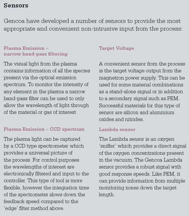
5 Reactive gas process controllers


6 Reactive gas process controllers Speedflo used in glass, solar, display & OLED sectors & makes today s & tomorrow s products possible
7 Coating ra te ( nm. m /m in) Si and SiOx rates at 23 kw (dual rotatable) Setpoint (O2 emission 777nm) Cost of ownership of reactive feedback elements Line speed increase x 3-5 Return on Speedflo (reactive controller) investment < 30 days

8 Reactive Sputtering Monitoring Exhaust Part. Press. Voltage, Freq. Plasma emmission Target Substrate Reactive gas input Transp.,σ,n Control
9 Process Inputs / Outputs Inputs PEM - Plasma emission monitor Metal line / multiple lines Gas line Argon line Plasma spectrum Target voltage Outputs (Actuator) Reactive Gas Flow Target Voltage Target Power Output Gas partial pressure (Ar / throttle valve) lambda sensor gas partial pressure
10 Pro / Cons of Inputs Inputs PEM - Plasma emission monitor Metal line / multiple lines Gas line Argon line Plasma spectrum Target voltage lambda sensor gas partial pressure PEM high speed, most universal / powerful & can be multi-zone but requires fibreoptics Target voltage is high speed and low cost but single zone and in the past for certain material / gas combinations Gas partial pressure - multigas expensive, but single gas lower cost, requires sensor in chamber
 Reactive Gas")

11 The ideal controller handles all Inputs PEM Metal line / multiple lines Gas line Argon line Plasma spectrum Target voltage Gas partial pressure Outputs (Actuator) Reactive Gas Flow Target Voltage Target Power Output Gas partial pressure (Ar / throttle valve) Why is Mulit-function important? Some processes are hard to control and drifts / fluctuations occur

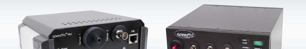
12 Speedflo multi-channel controller

13 Reactive deposition A ready made solution Large area reactive sputtering 30 years old Mature processing products available Reactive sputtering in the high rate metal mode is highly unstable process so appropriate process control the critical factor Gencoa have implemented reactive process control over many different production plants with > 3m glass sizes More than 500 Speedflo systems controlling reactive production plants around the world Gencoa can set-up the process control on-site or connect remotely to the Speedflo box

14 The data processing in the Speedflo box (not PC) for high speed robust operation Digital software drive process controller Typical closed loop feedback times of 5-20 msec from signal receipt to gas delivery in the target area.


15 Multiple sensors control and trim gas over large areas ±1.5% uniformity already commonplace on 1-3m glass Lambda Sensors Choice of sensor types available
16

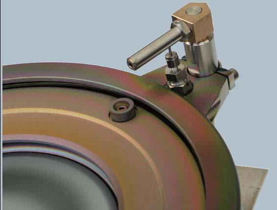
17 P.E.M requires the light signal from the plasma to be transmitted Gencoa have a range of optical components


18 Standard range of internal optical components and an external KF25 based sensor


19 Penning Gauge based P.E.M. sensor used for batch processes with plasma fluctuations Measures excess gas in the process
20 P.E.M, gas pipes and bars provide ~ 10msec process feedback response Gas bar design delivers gas quickly and uniformly Lambda sensors shown


21 Gas bar options and magnetically guided anodes are available to further enhance the performance of your process

22 Speedflo spectrometer based sensor displays the full plasma spectrum information Upto 4 different wavelengths can be combined


23 Gencoa Lambda sensors measure the O2 concentration in the vacuum chamber Additional sensor control box included


24 Different sensor control modes possible for reactive AZO via feedback controller O 2 gas Penning-PEM Lambda Target V Process- PEM

25 Speedflo different sensor responses to a gas ramp - hysteresis
26 The gas flow valves need to have a fast enough response to match the process needs The MKS 1179A is a suitable valve 5 4 Sensor 1 (PENNING) Actuator 1 (METER) Setpoint 1 Sensor 2 (LAMBDA) Actuator 2 (MFC) Setpoint msec

27 Gencoa will advise on with PEM sensor locations and gas delivery method & the sizes of the MFC s required for the process

28 All components need to be integrated correctly to ensure optimum operation
29 Reactive AZO Sputtering Hysteresis but can be controlled with feedback ZnAl dual rotatable + O 2 - TRIPLE RAMP CONDITIONING Signals, % Time, s SetPoint (%) Sensor (%) Actuator (%)

30 Process control window for Speedflo related to response for SiOx in typical AR layer stack for flat screen television
31
32 Example of controlled reactive dual rotatable ITO deposition runs InSn + O 2 Speedflo control during production tests Signals % Transmission 13Ω Sheet resistance time, s Sensor (V) Actuator (V) SetPoint (V)
33 Reactive dual rotatable AZO deposition process window Process control using plasma monitoring ZnAl + O 2 reactive control dual rotatable MFC feedback, sccm Gas Feedback (SCCM) O2 PEM value % O2 PEM setpoint % O2 PEM and target V Sensors (%) 10 Target V % Time, s
34 TCO film property tuning using Speedflo reactive sputtering controller with a dual rotatable magnetron InSn+O 2 using Speedflo control for reactive production of ITO Sheet resistance (ohms) Optimised Development Sheet resistance Transmission Transmission (%) O 2 Set-point (%)
35 The controller requires tuning to provide optimum control reactive AZO sputtering controller with a dual rotatable magnetron ZnAl + O2 reactive control dual rot rotatable MFC feedback, sccm Changed Ks to regain control Time, s Gas Feedback (SCCM) O2 PEM value % O2 PEM setpoint % O2 PEM and target V Sensors %
36 P.E.M based reactive sputtering controllers already work in large scale Low-E glass P.E.M control response to load-lock activity SiOx AC dual 3 Master (A, B & C) and 1 slave (1G) control Sensor B setpoint = 50% Sensor B(%) Sensor target V(%) Actuator 2B(%) Actuator 1G(%) Sensor sig nals target voltage variation Slave O 2 flow 1G=2 x (2B) Actuator sig nal % Master O 2 flow (2B) Time, s
37 Rate enhancement for reactive sputtering controllers Si and SiOx rates at 23 kw (dual rotatable) P.E.M set-point verses dynamic deposition rate 120 Coating ra te ( n m. m /m in ) Setpoint (O2 emission 777nm)
38 Rate enhancement for reactive sputtering controllers P.E.M set-point verses dynamic deposition rate AlO x depasition rate. Dual rotatable magnetron Target voltage setpoint, % Deposition rate (A.U.)
39 Rate or layer properties determine the controller set-point NbOx-SiOx layer gain in thickness after climate tests nm after climate test Layer thickness, nm nm after climate test NbOx (SiOx at 45%) NbOx (SiOx at 60%) SiOx at 45%PEM SiOx at 60%PEM 0 KT1_1 KT1_2 KT1_3 KT1_4 KT1_5 KT1_6 KT1_7 Sample reference

40 On-site process training and support by Gencoa personnel From UK office or local GENCOA employees


41 Gencoa provide process controllers, remote access or on-site process tuning Typical AR production line Speedflo installation


42 Rotatable & planar sputtering modules with speedflo control available


43 Complete process control modules including electronics Rear cabinet will house all the control and components


44 PEM sensors have argon bleed lines (not shown) to prevent coating of the optics All parts have been positioned for optimum process operation
45 Gencoa can provide a range of process control solutions based upon the Speedflo system for high rate oxide & nitride layers. As an example with the DLIM magnets, Speedflo controller and Gencoa gas bars a rate of between 40nm.m/min and 60nm.m/min will be achieved for SiO2 from 1 dual magnetron pair running at around 15kW AC per m length of target. The actual rate will be 40-55nm.m/min and will depend upon the coating properties required from the film. Gencoa can offer on-site process implementation and optimization based upon many years of experience on a wide range of processes and machine platforms. Conclusions
Using a standard Penning Gauge as a powerful means of monitoring and feedback control
 Gencoa - Dermot Monaghan Using a standard Penning Gauge as a powerful means of monitoring and feedback control Victor Bellido-González, Sarah Powell, Benoit Daniel, John Counsell, Dermot Monaghan Structure
Maximizing the Potential of Rotatable Magnetron Sputter Sources for Web Coating Applications
 Maximizing the Potential of Rotatable Magnetron Sputter Sources for Web Coating Applications V.Bellido-Gonzalez, Dermot Monaghan, Robert Brown, Alex Azzopardi, Gencoa, Liverpool UK Structure of presentation
Cracker valve and plasma control process for reactive sputtering with Selenium & Sulphur
 Cracker valve and plasma control process for reactive sputtering with Selenium & Sulphur Victor Bellido-González, Dermot Monaghan, Benoit Daniel, Joseph Brindley, Gencoa Ltd, UK Dr. Iván Fernández- Martínez,
Gencoa Product Portfolio
 Gencoa offer the following range of products & process technology for the thin film industry developed over the last 20 years Planar Magnetrons Plasma Pre- Treaters Reactive Gas Controllers Gencoa Product
Managing Anode Effects and Substrate Heating from Rotatable Sputter Targets
 Managing Anode Effects and Substrate Heating from Rotatable Sputter Targets Frank Papa*, Dermot Monaghan**, Victor Bellido- González**, and Alex Azzopardi** *Gencoa Technical & Business Support in US,
Large Area Coating for Glazing IOP Vacuum Symposium Daresbury 11 th Feb 2010
 Large Area Coating for Glazing IOP Vacuum Symposium Daresbury 11 th Feb 2010 Off-Line Coatings Technology Group Pilkington European Technology Centre 2 NSG Group Pilkington a member of NSG Group from June
Linear Plasma Sources for Surface Modification and Deposition for Large Area Coating
 Linear Plasma Sources for Surface Modification and Deposition for Large Area Coating Dr Tony Williams Gencoa Ltd, UK Victor Bellido-Gonzalez, Dr Dermot Monaghan, Dr Joseph Brindley, Robert Brown SVC 2016,
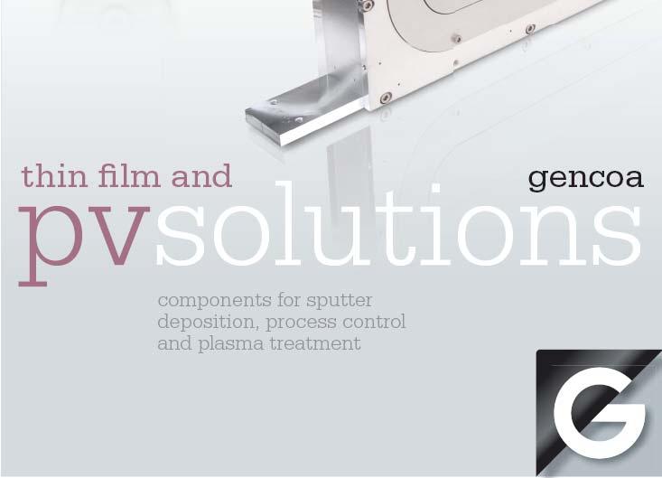
GENCOA. Perfect your process
 GENCOA Perfect your process 02 Introduction Providing expert solutions to a worldwide customer base over three decades, Gencoa is among the world leaders in the design and manufacture of products for the
Power Vision Ltd. PV Research. Power Vision Ltd. Unit R2, Herald Park, Crewe, Cheshire, CW1 6EA, UK Tel:
 Power Vision Ltd PV Research Power Vision Ltd Unit R2, Herald Park, Crewe, Cheshire, CW1 6EA, UK www.pvoptical.com Tel: +44 1270 253000 Flexible Whether it be fast AR coating onto temperature sensitive
HiPIMS Deposition of Metal and Oxide Coatings
 HiPIMS Deposition of Metal and Oxide Coatings 1 GT West, 1 PJ Kelly, 1 P Barker, 2 JW Bradley and 2 A Mishra 1. Surface Engineering Group, Manchester Metropolitan University, UK 2. Electrical Engineering
Roll-to-roll Technology for Transparent High Barrier Films
 Roll-to-roll Technology for Transparent High Barrier Films Presented at the AIMCAL Fall Technical Conference, October 19-22, 2008, Myrtle Beach, SC, USA Nicolas Schiller, John Fahlteich, Matthias Fahland,
Plasma Quest Limited
 Plasma Quest Limited A Remote Plasma Sputter Process for High Rate Web Coating of Low Temperature Plastic Film with High Quality Thin Film Metals and Insulators Dr. Peter Hockley and Prof. Mike Thwaites,
New Dual Magnetron Plasma Source Designed For Large Area Substrate Pretreatment and Oxide Film Deposition P. Morse, R. Lovro, M. Rost, and J.
 New Dual Magnetron Plasma Source Designed For Large Area Substrate Pretreatment and Oxide Film Deposition P. Morse, R. Lovro, M. Rost, and J. German, Road Map Source Design Theory of Operation Experimental
AC Reactive Sputtering with Inverted Cylindrical Magnetrons
 AC Reactive Sputtering with Inverted Cylindrical Magnetrons D.A. Glocker, Isoflux Incorporated, Rush, NY; and V.W. Lindberg and A.R. Woodard, Rochester Institute of Technology, Rochester, NY Key Words:
Barrier Coating Encapsulation Using Rotatable Cylindrical Sputtering Cathodes
 Barrier Coating Encapsulation Using Rotatable Cylindrical Sputtering Cathodes V. Bellido-Gonzalez, D. Monaghan, R. Brown, B. Daniel, J. Brindley, A. Azzopardi, and I. Sorzabal-Bellido, Gencoa Ltd., Liverpool,
Comparison of Different Sputter Processes for ITO: Planar DC versus Planar AC
 Comparison of Different Sputter Processes for ITO: Planar DC versus Planar AC P. Sauer,H.-G.Lotz, A. Hellmich R. Kukla, J. Schröder Applied Films GmbH &,Co. KG, Alzenau, Germany Outline n n n n n n Current
Comparison of Different Sputter Processes for ITO: Planar DC versus Planar AC
 Comparison of Different Sputter Processes for ITO: Planar DC versus Planar AC P. Sauer, H.-G. Lotz, A. Hellmich, R. Kukla, J. Schröder Applied Films GmbH & Co. KG, Alzenau, Germany Key Words: ITO MF PET
High Rate Deposition of Reactive Oxide Coatings by New Plasma Enhanced Chemical Vapor Deposition Source Technology
 General Plasma, Inc. 546 East 25th Street Tucson, Arizona 85713 tel. 520-882-5100 fax. 520-882-5165 High Rate Deposition of Reactive Oxide Coatings by New Plasma Enhanced Chemical Vapor Deposition Source
Solar Selective Absorber Coating Methods Plasma Processes
 Solar Selective Absorber Coating Methods Plasma Processes Paul Gantenbein & Elimar Frank SPF - Institut für Solartechnik University of Applied Sciences Rapperswil (HSR) Optical properties of a selective
Photovoltaics & Solar Thermals. Thin-film equipment. Customized. FHR Anlagenbau GmbH I
 Photovoltaics & Solar Thermals Thin-film equipment. Customized. FHR Anlagenbau GmbH I www.fhr.de FHR Anlagenbau GmbH is an innovative enterprise in the branch of vacuum processing and thin-film technologies.
Advanced Glass Refinement by Thin Films - Trends and Challenges of Thin Film Technologies for Windows and Facade Glasses
 Advanced Glass Refinement by Thin Films - Trends and Challenges of Thin Film Technologies for Windows and Facade Glasses Dr.-Ing. Manuela Junghähnel Fraunhofer Institute for Elect ron Beam and Plasma Technology
Inline Sputtering System for Heterojunction Cells
 GENERIS PVD Inline Sputtering System for Heterojunction Cells GENERIS PVD Inline Sputter System for ITO and Ag Deposition on Heterojunction Solar Cells Sputtering Technology at a Glance has delivered far
Mass Production of Clear Barriers. Requirements on Vacuum Web Coaters for Quality Assurance. Rainer Ludwig, Applied Films, Alzenau, Germany.
 Mass Production of Clear Barriers Requirements on Vacuum Web Coaters for Quality Assurance Rainer Ludwig, Applied Films, Alzenau, Germany Abstract An increasing number of packages using Transparent Barrier
Vacuum Equipment for TCO and AR Coatings Deposition by Reactive Magnetron Sputtering
 Vacuum Equipment for TCO and AR Coatings Deposition by Reactive Magnetron Sputtering E. Yadin; V. Kozlov; E. Machevskis, Sidrabe, Inc., 17 Krustpils str.,riga, LV1073, Latvia. Tel: +371 7249806, Fax: +371
Vacuum Deposition of High Performance Gas Barrier Materials for Electronics Applications
 Vacuum Deposition of High Performance Gas Barrier Materials for Electronics Applications Hélène Suttle DPhil Research Student Department of Materials -University of Oxford AIMCAL Fall Conference October
Intlvac Nanochrome I Sputter System (intlvac_sputter)
") 1. Intlvac_Sputter Specifications The Intlvac Nanochrome I sputter system is configured for DC, AC (40 khz), and RF (13.56 MHz) magnetron sputtering. They system has in-situ quartz lamp heating up to 200C,
1. Intlvac_Sputter Specifications The Intlvac Nanochrome I sputter system is configured for DC, AC (40 khz), and RF (13.56 MHz) magnetron sputtering. They system has in-situ quartz lamp heating up to 200C,
Denton 635 Sputter SOP
 Denton 635 SOP Page 1 of 8 Denton 635 Sputter SOP 1. Scope 1.1 This document provides operating procedures for the Denton 635 automated sputter system.. 2. Table of Contents 1. Scope... 1 2. Table of Contents...
High Performance Optical Coatings Deposited Using Closed Field Magnetron Sputtering
 High Performance Optical Coatings Deposited Using Closed Field Magnetron Sputtering D.R. Gibson, I.T. Brinkley, and J.L. Martin Applied Multilayers LLC, 1801 SE Commerce Avenue, Battle Ground, WA 98604
A Design for an efficient cylindrical magnetron cathode with rotating magnets and optical emission incorporated
 Patent on, A Design for an efficient cylindrical magnetron cathode with rotating magnets and optical emission incorporated Inventors A. Subrahmanyam, Krishna Valleti IIT Madras, Chennai, INDIA. Shrikanth
Energy Efficient Glazing Design. John Ridealgh Off-Line Coatings Technology Group Pilkington European Technology Centre
 Energy Efficient Glazing Design John Ridealgh Off-Line Coatings Technology Group Pilkington European Technology Centre 2 John Ridealgh 30th November 2009 Talk Outline Pilkington Group Limited & NSG Group
ITO SPUTTER COATED FILMS FOR TOUCH PANEL APPLICATIONS USING ROTARY SINTERED CERAMIC ITO TARGETS: WHAT CAN BE LEARNED FROM GLASS COATING?
 ITO SPUTTER COATED FILMS FOR TOUCH PANEL APPLICATIONS USING ROTARY SINTERED CERAMIC ITO TARGETS: WHAT CAN BE LEARNED FROM GLASS COATING? Paul Lippens AIMCAL Web coating conference 2012 Outline Introduction
Nanoparticle generation using sputtering plasmas
 NCCAVS Joint Users Group Technical Symposium Nanomaterials for Energy, Biomedical, and Electronic Devices In Conjunction with the NCCAVS 35th Annual Equipment Exhibition Nanoparticle generation using sputtering
Thin Films: Sputtering Systems (Jaeger Ch 6 & Ruska Ch 7,) Can deposit any material on any substrate (in principal) Start with pumping down to high
 Can deposit any material on any substrate (in principal) Start with pumping down to high") Thin Films: Sputtering Systems (Jaeger Ch 6 & Ruska Ch 7,) Can deposit any material on any substrate (in principal) Start with pumping down to high vacuum ~10-7 torr Removes residual gases eg oxygen from
Thin Films: Sputtering Systems (Jaeger Ch 6 & Ruska Ch 7,) Can deposit any material on any substrate (in principal) Start with pumping down to high vacuum ~10-7 torr Removes residual gases eg oxygen from
GENERIS PVD. Inline Sputtering System for Heterojunction Solar Cells
 GENERIS PVD Inline Sputtering System for Heterojunction Solar Cells GENERIS PVD Inline Sputtering System for Heterojunction Solar Cells Sputtering Competence has delivered far more than 8000 vacuum sputtering
Improvement of gas barrier properties by combination of polymer film and gas barrier layer
 Improvement of gas barrier properties by combination of polymer film and gas barrier Y. Tsumagari, H. Murakami, K. Iseki and S. Yokoyama Toyobo Co., LTD. RESEARCH CENTER, - Katata 2-chome, Otsu, Shiga,
Ion-plasma technologies and equipment
 Ion-plasma technologies and equipment VACUUM ION-PLASMA INSTALLATIONS OF «OPAL» SERIES «Opal» series ion-plasma installations are designed for deposition of low-emission, reflective and toned coatings
Previous Lecture. Vacuum & Plasma systems for. Dry etching
 Previous Lecture Vacuum & Plasma systems for Dry etching Lecture 9: Evaporation & sputtering Objectives From this evaporation lecture you will learn: Evaporator system layout & parts Vapor pressure Crucible
Properties of Highly Transparent Conductive Ga-Doped ZnO Films prepared on Polymer Substrates by Reactive Plasma Deposition with DC Arc Discharge
 Journal of Photopolymer Science and Technology Volume 22, Number 4 (2009) 497-502 2009 CPST Properties of Highly Transparent Conductive Ga-Doped ZnO Films prepared on Polymer Substrates by Reactive Plasma
Applied Research for Vacuum Web Coating: What is Coming Next?
 Applied Research for Vacuum Web Coating: What is Coming Next? Matthias Fahland, John Fahlteich, Steffen Günther, Manuela Junghähnel, Claus Luber, Nicolas Schiller, Cindy Steiner, Steffen Straach, Michiel
Improving coupling coefficient distribution on BAW filters manufactured on 200mm wafers
 Improving coupling coefficient distribution on BAW filters manufactured on 200mm wafers Sergey Mishin Advanced Modular Systems, Inc Goleta, CA/USA smishin@amssb.com Yury Oshmyansky Advanced Modular Systems,
Atomic Layer Deposition. ALD process solutions using FlexAL and OpAL
 Atomic Layer Deposition process solutions using FlexAL and OpAL Introduction to Self limiting digital growth Atomic Layer Deposition () offers precisely controlled ultra-thin films for advanced applications
the Netherlands Key words: Sputtering Deposition; ZnO; Resistivity; Transmittance
 Advanced Materials Research Online: 011-0-1 ISS: 1-95, Vols. 19-19, pp 7-75 doi:.0/www.scientific.net/amr.19-19.7 011 Trans Tech Publications, Switzerland Electrical and Optical Properties of Indium and
Characterisation studies of the pulsed dual cathode magnetron sputtering process for oxide films
 Surface and Coatings Technology 142 144 2001 621 627 Characterisation studies of the pulsed dual cathode magnetron sputtering process for oxide films J. O Brien, P.J. Kelly Centre for Materials Research,
ZnO-based Transparent Conductive Oxide Thin Films
 IEEE EDS Mini-colloquium WIMNACT 32 ZnO-based Transparent Conductive Oxide Thin Films Weijie SONG Ningbo Institute of Material Technology and Engineering, Chinese Academy of Sciences, Ningbo, P. R. China
Energy-efficient glazing
 Energy-efficient glazing Low-E solar reflective coatings Float glass is traditionally used in the building and automotive industries to provide both clear and tinted transparent barriers to the elements.
Ellipsometry as a tool for identifying process issues in roll-to-roll sputter deposited metal-oxide coatings
 Ellipsometry as a tool for identifying process issues in roll-to-roll sputter deposited metal-oxide coatings Sharon Louch Centre for Process Innovation, Wilton Centre, edcar. UK. TS10 3H Abstract Ellipsometry
Photovoltaics. Thin film equipment from Oxford Instruments. The Business of Science
 Photovoltaics Thin film equipment from Oxford Instruments The Business of Science Photovoltaics Plasmalab System100Pro and Plasmalab System133Pro Flexible systems for front end PV research With over 20
PEAK EFFICIENCIES WITH FALLING MANUFACTURING COSTS
 PEAK EFFICIENCIES WITH FALLING MANUFACTURING COSTS Simple and cost-effective introduction of PERC technology into the mass production of solar cells Kerstin Strauch, Florian Schwarz, Sebastian Gatz 1 Introduction
SPUTTERING TECHNOLOGY. for Multiple Applications such as Solar, Display, Semiconductor & 3D-Substrates
 SPUTTERING TECHNOLOGY for Multiple Applications such as Solar, Display, Semiconductor & 3D-Substrates 02 Over 20 Years of Know-how in Physical Vapor Deposition Sputtering PECVD Evaporation SINGULUS TECHNOLOGIES
Durable Neutral Color Anti-Reflective Coating for Mobile Displays
 Durable Neutral Color Anti-Reflective Coating for Mobile Displays By John Madocks and Phong Ngo, General Plasma, Inc. Figure 1: Samsung S4 with top half of cover glass coated with AR+DLC Abstract An in-line
Deposited by Sputtering of Sn and SnO 2
 Journal of the Korean Ceramic Society Vol. 49, No. 5, pp. 448~453, 2012. http://dx.doi.org/10.4191/kcers.2012.49.5.448 Comparative Study of Nitrogen Incorporated SnO 2 Deposited by Sputtering of Sn and
BAK EVAPORATOR FAMILY
 BAK EVAPORATOR FAMILY THE BAK A NEW GENERATION TAKING THE BEST FROM THE PAST, EXPANDING YOUR HORIZONS FOR THE FUTURE! The BAV 2000 - a production giant 2000 BAK SYSTEMS DELIVERED WORLDWIDE 2 BAK EVAPORATOR
Hafnium oxide thin films deposited by reactive middle-frequency dual-magnetron sputtering
 Thin Solid Films 515 (2007) 7984 7989 www.elsevier.com/locate/tsf Hafnium oxide thin films deposited by reactive middle-frequency dual-magnetron sputtering V. Pervak a,, F. Krausz a,b, A. Apolonski b,c
Optical Coatings. Photonics 4 Luxury Coatings , Genève. Dr. Andreas Bächli Head of Optical Coatings at RhySearch, Buchs (SG)
") Optical Coatings Photonics 4 Luxury Coatings 21.06.2017, Genève Dr. Andreas Bächli Head of Optical Coatings at RhySearch, Buchs (SG) RhySearch The Research- and Innovation Center in the Rhine Valley RhySearch
Optical Coatings Photonics 4 Luxury Coatings 21.06.2017, Genève Dr. Andreas Bächli Head of Optical Coatings at RhySearch, Buchs (SG) RhySearch The Research- and Innovation Center in the Rhine Valley RhySearch
Atomic Layer Deposition (ALD)
") Atomic Layer Deposition (ALD) ALD provides Uniform, controlled, conformal deposition of oxide, nitride, and metal thin films on a nanometer scale. ALD is a self limiting thin film deposition technique
Atomic Layer Deposition (ALD) ALD provides Uniform, controlled, conformal deposition of oxide, nitride, and metal thin films on a nanometer scale. ALD is a self limiting thin film deposition technique
Combinatorial RF Magnetron Sputtering for Rapid Materials Discovery: Methodology and Applications
 Combinatorial RF Magnetron Sputtering for Rapid Materials Discovery: Methodology and Applications Philip D. Rack,, Jason D. Fowlkes, and Yuepeng Deng Department of Materials Science and Engineering University
Oerlikon PVD production solution for in-situ large scale deposition of PZT
 Oerlikon PVD production solution for in-situ large scale deposition of PZT 2nd International Workshop on Piezoelectric MEMS Materials - Processes - Tools - Devices Lausanne, 06./07.09.2011 M. Kratzer,
CONFERENCE EVALUATION FORM
 2015 AIMCAL Web Coating & Handling / SPE FlexPackCon CONFERENCE EVALUATION FORM To upgrade the quality of the Web Coating & Handling / FlexPackCon Conference, we would appreciate your comments. MONDAY,
BAK. Evaporator Family
 BAK Evaporator Family The BAK A new generation Taking the best from the past, expanding your horizons for the future! More than 1500 systems worldwide 2 BAK Evaporator Family more choice than ever Welcome
Plasma-Enhanced Chemical Vapor Deposition
 Plasma-Enhanced Chemical Vapor Deposition Steven Glenn July 8, 2009 Thin Films Lab 4 ABSTRACT The objective of this lab was to explore lab and the Applied Materials P5000 from a different point of view.
Thin Films: Sputtering Systems (Jaeger Ch 6 & Ruska Ch 7,) Sputtering: gas plasma transfers atoms from target to substrate Can deposit any material
 Sputtering: gas plasma transfers atoms from target to substrate Can deposit any material") Thin Films: Sputtering Systems (Jaeger Ch 6 & Ruska Ch 7,) Sputtering: gas plasma transfers atoms from target to substrate Can deposit any material on any substrate (in principal) Start with pumping down
Thin Films: Sputtering Systems (Jaeger Ch 6 & Ruska Ch 7,) Sputtering: gas plasma transfers atoms from target to substrate Can deposit any material on any substrate (in principal) Start with pumping down
Manufacturability of highly doped Aluminum Nitride films
 Manufacturability of highly doped Aluminum Nitride films Sergey Mishin Yury Oshmyansky Advanced Modular Systems, Inc Goleta, CA/USA smishin@amssb.com yoshmyansky@amssb.com Abstract There have been several
Effective Closed-Loop Control for Reactive Sputtering Using Two Reactive Gases
 Effective Closed-Loop Control for Reactive Sputtering Using Two Reactive Gases D.C. Carter, W.D. Sproul, and D.J. Christie, Advanced Energy Industries, Inc., Fort Collins, CO Key Words: Reactive sputtering
High rate reactive magnetron sputtering of ZnO:Al films from rotating metallic targets
 High rate reactive magnetron sputtering of ZnO:Al films from rotating metallic targets H. Zhu 1, 2, *, J. Hüpkes 1, E. Bunte 1 1 IEF5-Photovoltaik, Forschungszentrum Jülich GmbH, D-52425 Jülich, Germany
Gridless end-hall. Ion Sources. For Ion Assisted Thin Film Deposition & Substrate Cleaning
 Gridless end-hall Ion Sources For Ion Assisted Thin Film Deposition & Substrate Cleaning End-Hall Ion Sources mark I Ion Source The Mark I End-Hall is ideal for small research and development and pilot
EQUIPMENT EQUIPMENT FOR HIGH-EFFICIENCY SOLAR CONCEPTS CRYSTALLINE SILICON PV. SCALA XEA nova XENIA
 CRYSTALLINE SILICON PV EQUIPMENT EQUIPMENT FOR HIGH-EFFICIENCY SOLAR CONCEPTS SCALA XEA nova XENIA VON ARDENNE was founded in 1991 as a spin-off of the former Manfred von Ardenne Research Institute. The
A Plasma Emission Controller for Reactive. Magnetron Sputtering of Titanium Dioxide Films
 Adv. Theor. Appl. Mech., Vol. 5, 2012, no. 1, 1-10 A Plasma Emission Controller for Reactive Magnetron Sputtering of Titanium Dioxide Films Raad A. Swady DMPS, College of Arts & Sciences, University of
An innovative approach to coatings on large optics
 An innovative approach to coatings on large optics OpTIC Strategic Conference 16 th -17 th November 2010 "Photographie: Philippe Bourgeois" CILAS - Établissement Marseille Z.I. St Mitre 15 avenue de la
High Rate low pressure PECVD for barrier and optical coatings
 High Rate low pressure PECVD for barrier and optical coatings, Matthias Fahland, John Fahlteich, Björn Meyer, Steffen Straach, Nicolas Schiller Outline Introduction PECVD New developments magpecvd arcpecv
Extending Etch and Deposition Capabilities for Implementation of 3D Packaging of MEMS in Volume Production
 Extending Etch and Deposition Capabilities for Implementation of 3D Packaging of MEMS in Volume Production David Butler, VP Product Management & Marketing SPTS Technologies Contents Industry Trends TSV
Metallization deposition and etching. Material mainly taken from Campbell, UCCS
 Metallization deposition and etching Material mainly taken from Campbell, UCCS Application Metallization is back-end processing Metals used are aluminum and copper Mainly involves deposition and etching,
Innovative Laser Processing Technologies
 Innovative Laser Processing Technologies Reinhard Ferstl Director Sales & Marketing EMEA / Asia Corning Laser Technologies September 21, 2016 2016 Corning Incorporated Corning Market Segments and Additional
Study on Properties of Silicon Oxycarbide Thin Films Prepared by RF Magnetron Sputtering Tao Chen a, Maojin Dong, Jizhou Wang,Ling Zhang and Chen Li
 Study on Properties of Silicon Oxycarbide Thin Films Prepared by RF Magnetron Sputtering Tao Chen a, Maojin Dong, Jizhou Wang,Ling Zhang and Chen Li Science and Technology on Surface Engineering Laboratory,
Model TEM Mill. Tabletop precision preparation for producing high-quality TEM specimens from a wide variety of materials EXCELLENCE MAGNIFIED
 Model 1050 TEM Mill Tabletop precision preparation for producing high-quality TEM specimens from a wide variety of materials EXCELLENCE MAGNIFIED Modular design for basic instrument operation or fully
Oerlikon PVD production solutions for piezoelectric materials
 Oerlikon PVD production solutions for piezoelectric materials Workshop PiezoMEMS Aachen,18. /19.05.2010 M. Kratzer Oerlikon Systems R&D Oerlikon company and products Thin films used for SAW, BAW, MEMS,
Optimization of the Sputtering Process for Depositing Composite Thin Films
 Journal of the Korean Physical Society, Vol. 40, No. 3, March 2002, pp. 511 515 Optimization of the Sputtering Process for Depositing Composite Thin Films M. Farooq Pakistan Council of Renewable Energy
Productivity versus Profitability in Vacuum Web Coating
 Productivity versus Profitability in Vacuum Web Coating Liz Josephson, Applied Films Corp., Longmont, USA Dirk Hoffmann, Applied Films GmbH & Co KG, Alzenau, Germany Gerard Loebig, Applied Films GmbH &
1 Introduction. 2 Basic Technology
 Innovative Clear Barrier Technology for the Packaging Industry Nicolas Schiller 1, Steffen Straach, Steffen Günther Fraunhofer FEP, Germany Alexandra L. Quiceno G., Antonio García Contreras BIOFILM, Columbia
Transparent Heat Mirror Using Plasma Polymer Fluorocarbon Fabricated by Continuous Roll-to-Roll Sputtering
 2R Conference USA 2018 Transparent Heat Mirror Using Plasma Polymer Fluorocarbon Fabricated by Continuous Roll-to-Roll Sputtering Sang-Jin Lee, Ph.D/Principal Researcher Sung Hyun Kim, Mac Kim, Tae-Woon
Thin Films & AR Coated. Viewports. Thin Film & AR Coated. Viewports
 Thin Films & AR Item Page Thin Film Coatings Introduction P 02 Kodial Zero Length with Anti-Reflective Coatings P 04 Kodial Zero Length with Anti-Reflective Coatings-Non-Magnetic P 07 Kodial Zero Length
Latest Development in Vacuum Metallisation
 Latest Development in Vacuum Metallisation Professor Nadir Ahmed Vacuum Metallising Consultant General Vacuum Equipment Ltd. Pennine Business Park, Pilsworth Road, Heywood OL10 2TL England Tel: +44(0)1706
Fullerene-like Carbon Nitride Coatings: From Lab-scale Research to Industrial-scale Production
 Fullerene-like Carbon Nitride Coatings: From Lab-scale Research to Industrial-scale Production Prof. Esteban Broitman Prof. Esteban Broitman Thin Films Physics Division, IFM, Linköping University, Sweden
The Improvement in Energy Efficiency Based on Nano-structure Materials
 International Workshop on 1iGO Science and Technology 2010 The Improvement in Energy Efficiency Based on Nanostructure Materials Chien Chon Chen Department of Energy and Resources, National United University,
Development of Conductive Polymer Film and R2R Coating Process
 Development of Conductive Polymer Film and R2R Coating Process Nizamidin Jappar; Ph.D. General Manager of R&D Kimoto Tech Inc. AIMCAL Web Coating & Handling Conference Outline 1 Background 2 3 4 Develop
PlasmaPro TM System100 & System133. Modular tools for wafer processing100
 TM System100 & System133 Modular tools for wafer processing100 System100 & System133 Plasma etch & deposition process modules Oxford Instruments System100 and System133 process modules are built on 200mm
PRECISION OPTICAL FILTERS BY EOSS - ENHANCED OPTICAL SPUTTERING SYSTEM. Fraunhofer
 PRECISION OPTICAL FILTERS BY EOSS - ENHANCED OPTICAL SPUTTERING SYSTEM EOSS ENHANCED OPTICAL SPUTTERING SYSTEM Fraunhofer IST, Braunschweig Contact: Dr. M. Vergöhl +49 531 2155 640 EOSS Coating System
Si DRIE APPLICATION In Corial 210IL
 Si DRIE APPLICATION In Corial 210IL CORIAL 210IL ICP-RIE equipment for deep Si etching applications Enlarged functionality with capability to deep etch silicon, silicon carbide, glass, sapphire, and quartz
THE INCREASE IN THICKNESS UNIFORMITY OF FILMS OBTAINED BY MAGNETRON SPUTTERING WITH ROTATING SUBSTRATE
 Plasma Physics and Technology 3(3):1 14, 216 Department of Physics, FEE CTU in Prague, 216 THE INCREASE IN THICKNESS UNIFORMITY OF FILMS OBTAINED BY MAGNETRON SPUTTERING WITH ROTATING SUBSTRATE Golosov
Chapter 3 Silicon Device Fabrication Technology
 Chapter 3 Silicon Device Fabrication Technology Over 10 15 transistors (or 100,000 for every person in the world) are manufactured every year. VLSI (Very Large Scale Integration) ULSI (Ultra Large Scale
BAK EVAPORATOR FAMILY
 BAK EVAPORATOR FAMILY THE BAK A NEW GENERATION TAKING THE BEST FROM THE PAST, EXPANDING YOUR HORIZONS FOR THE FUTURE! The BAV 2000 - a production giant 2000 BAK SYSTEMS DELIVERED WORLDWIDE 2 BAK EVAPORATOR
Lecture Day 2 Deposition
 Deposition Lecture Day 2 Deposition PVD - Physical Vapor Deposition E-beam Evaporation Thermal Evaporation (wire feed vs boat) Sputtering CVD - Chemical Vapor Deposition PECVD LPCVD MVD ALD MBE Plating
Excellent Plasma Control over Reactive Sputtering. Plasma Emission Controller
 Excellent Control over Reactive Sputtering Emission Controller The superb feedback control of the reactive gas flow in a reactive sputtering process helps you enhance product quality and achieve greater
Plasma Activated EB-PVD of Titanium and its Compounds by Means of Large Area SAD
 AIMCAL 2005 Myrtle Beach, SC, USA, October 19th, 2005 Plasma Activated EB-PVD of Titanium and its Compounds by Means of Large Area SAD E. Reinhold, C. Steuer VON ARDENNE Anlagentechnik GmbH, Dresden, Germany
Physical Vapor Deposition (PVD) Zheng Yang
 Zheng Yang") Physical Vapor Deposition (PVD) Zheng Yang ERF 3017, email: yangzhen@uic.edu Page 1 Major Fabrication Steps in MOS Process Flow UV light Mask oxygen Silicon dioxide photoresist exposed photoresist oxide
Physical Vapor Deposition (PVD) Zheng Yang ERF 3017, email: yangzhen@uic.edu Page 1 Major Fabrication Steps in MOS Process Flow UV light Mask oxygen Silicon dioxide photoresist exposed photoresist oxide
Excimer Laser Annealing of Hydrogen Modulation Doped a-si Film
 Materials Transactions, Vol. 48, No. 5 (27) pp. 975 to 979 #27 The Japan Institute of Metals Excimer Laser Annealing of Hydrogen Modulation Doped a-si Film Akira Heya 1, Naoto Matsuo 1, Tadashi Serikawa
Activities in Plasma Process Technology at SENTECH Instruments GmbH, Berlin. Dr. Frank Schmidt
 Activities in Plasma Process Technology at SENTECH Instruments GmbH, Berlin Dr. Frank Schmidt The Company Company Private company, founded 1990 80 employees ISO 9001 Location Science & Technology Park,
Barix Multilayers: a Water and Oxygen Barrier for Flexible Organic Electronics. Robert Jan Visser
 Barix Multilayers: a Water and Oxygen Barrier for Flexible Organic Electronics Robert Jan Visser Organic Electronics Is the Future of Electronics Organic? MIT Stanford UC Berkeley Nano Forum Vitex Systems,
Crystallization of Amorphous Silicon Thin Film. by Using a Thermal Plasma Jet. Hyun Seok Lee, Sooseok Choi, Sung Woo Kim, and Sang Hee Hong*
 Crystallization of Amorphous Silicon Thin Film by Using a Thermal Plasma Jet Hyun Seok Lee, Sooseok Choi, Sung Woo Kim, and Sang Hee Hong* Department of Nuclear Engineering, Seoul National University Seoul
"ITO Film Trend for Touch Panel Applications"
 AIMCAL Web Coating Conference 2011 October 23-26 Reno, Nevada USA 1 "ITO Film Trend for Touch Panel Applications" Teijin Chemicals Ltd. Haruhiko Itoh 2 Content 1. Structure and Features of TCF 2. Touch
Advanced Sheet-to-Sheet and Roll-to-Roll thin-film processing on ultra-thin flexible glass for flexible electronic devices
 Advanced Sheet-to-Sheet and Roll-to-Roll thin-film processing on ultra-thin flexible glass for flexible electronic devices M. Junghaehnel 1, J. Westphalen 1, F. Naumann 2, G. Lorenz 2, M. Fahland 1, S.