Advanced Lithography Updates and Challenges for Metrology and Inspection
|
|
|
- Lauren James
- 6 years ago
- Views:
Transcription
1 Advanced Lithography Updates and Challenges for Metrology and Inspection Center for Semiconductor Research & Development Advanced Lithography Process Technology Dept. Tatsuhiko Higashiki

2 Contents Device Roadmap and Lithography Extendibility toward 1x nm hp and beyond with New Lithography EUVL NIL DSA Conclusion 2
3 Contents Device Roadmap and Lithography Extendibility toward 1x nm hp and beyond with New Lithography EUVL NIL DSA Conclusion 3
4 Rapid Increase of Information Volume Demand All information that is created, captured, replicated and/or consumed by all human on the planet. 1ZB=1,000,000,000,000,000,000,000=10^21B Pressed by IDC on Jan.24, 2013 All information is not fully stored, but partially stored. Need for larger-capacity memory in the future. 4
, etc BiCS")
5 3D Roadmap of the Memory hp3xnm hp2xnm hp1xnm hp0xnm FG FG FG FG CG STI FG FG FG CG STI FG CG FG FG STI CP(Cross Point), etc BiCS 5
6 More than Moore Lithography Challenges ArF im NA>1~1.35 Light Source EUVL NA0.32 >0.4x? ArF im SADP More Moore hp56nm hp43nm hp32nm hp2xnm hp1xnm hp0xnm Tool Defect ML2 NIL Resist, Mask, Inspection, etc Cost EUVL+SADP EUVL+DSA ArF imsaqp/saop? Arf im SAQP+DSA NIL+DSA Performance & Economics ML2+DSA SADP : self-aligned double patterning SAQP : self-aligned quadruple patterning SAOP : self-aligned octuplet patterning 6
7 Contents Device Roadmap and Lithography Extendibility toward 1x nm hp and beyond with New Lithography EUVL NIL DSA Conclusion 7
8 More than Moore Lithography Challenges ArF im NA>1~1.35 Light Source EUVL NA0.32 >0.4x? ArF im SADP More Moore hp56nm hp43nm hp32nm hp2xnm hp1xnm hp0xnm Tool Defect ML2 NIL Resist, Mask, Inspection, etc Cost EUVL+SADP EUVL+DSA ArF imsaqp/saop? Arf im SAQP+DSA NIL+DSA Performance & Economics ML2+DSA SADP : self-aligned double patterning SAQP : self-aligned quadruple patterning SAOP : self-aligned octuplet patterning 8


9 EUVL and SADP Complementally dteos 加工後 hp14nm Exposure was Realized by EUVL + SADP EUVL Resist 28nm Spacer Film 14nm Si ウェハ hp28nm Spacer hp14nm Y. Watanabe et al, Photomask Japan 2010(April) 9
 Specification Design for Tools Mask process Resist process")

10 EUV Collaboration Device & design Si Process Lithography Pattern Layout Tech. (OPC/DFM) Specification Design for Tools Mask process Resist process Advanced EUVL Mask Quality Mask Inspections Resist Quality High NA Exposure Suppliers Exposure Tool EDA Resist Material Mask Metrology and Inspection 10


 2.0 2.0 2.5 3.")
11 EUV Source Roadmap HVM I HVM II HVM I 10 sources in operation 5 installed at Fabs 5 for development at Cymer / ASML HVM II 1 st source delivered Four in build EUV Source Power Roadmap Source Model HVM I HVM II HVM II HVM II Average Laser Power (kw) In-band CE (%) Clean EUV Power (W)

12 Current Situation of EUVL Light Source Let there be light and there was light "Fiat lux!" Et facta est lux. 12
13 Contents Device Roadmap and Lithography Extendibility toward 1x nm hp and beyond with New Lithography EUVL NIL DSA Conclusion 13
14 More than Moore Lithography Challenges ArF im NA>1~1.35 Light Source EUVL NA0.32 >0.4x? ArF im SADP More Moore hp56nm hp43nm hp32nm hp2xnm hp1xnm hp0xnm Tool Defect ML2 NIL Resist, Mask, Inspection, etc Cost EUVL+SADP EUVL+DSA ArF imsaqp/saop? Arf im SAQP+DSA NIL+DSA Performance & Economics ML2+DSA SADP : self-aligned double patterning SAQP : self-aligned quadruple patterning SAOP : self-aligned octuplet patterning 14
15 MII s Nano-Lithography Solution Jet and Flash Imprint Lithography (J-FIL) 6025 photomask substrate Mask Step 1: Dispense drops Step 2: Lower imprint mask and fill pattern Planarization layer Substrate Mask Planarization layer Substrate Major Advantages Lower cost of ownership - No laser, no track, no lenses, no vacuum No resolution limit by optical projection system Step 3: Polymerize fluid with UV exposure Step 4: Separate mask from substrate Planarization layer Substrate Mask Planarization layer Substrate Step & Repeat or whole wafer imprinting 15


16 Template Wafer Resolution of NIL Printing Template Wafer hp16nm hp24nm Spot Beam VSB 1Month/Shot 1day/Shot Ref. T.Higashiki, ,SPIE
 CDU(on wafer) 0.")
17 CDU Update of MII Tool Imprinted-shots Measured-Metric (12 sites/shot x 20 shots/wafer) CDU(on wafer) 0.5 nm(3σ) 17

18 Mix and Match Overlay X Y Raw Mean Raw 3sigma Mean + 3sigma Achieving less than 10nm 3sigma Mix and Match overlay Ref. T.Higashiki, ,SPIE


19 Counterme asure Example of Image Phenomenon Classification of Nanoimprint Defects 1.Non-fill 2.Template 3.Plug Defect Defect Defect Filling issue by remaining bubble Printed template defect Separation issue, pattern is torn off Template Improvement of the filling process Imprinted Pattern Improvement of template fabrication process Improvement of separation process and materials 19

20 Electrical Test for Overall Evaluation Test chip design Open Test snake pattern Short Test comb pattern 20
21 Yield Improving Imprint Electrical Yield Electrical Defect Testing: Yield vs. Line Length 100% 80% J-FIL 60% 40% 26nm HP 20% 0% Line Length (mm) Steady progress in electrical yield of imprint process. Results are encouraging and improving with mask replica defect improvements
22 Current Status of NIL Attribute Target Status Template Master CDU < 1.0nm 1.2nm Image Placement < 3nm(3σ) 2.5nm(3σ) Master Defectivity < 0.1/cm2 0-1/cm2 Replica Defectivity < 1/cm2 ~5/cm2 Imprint LER < 2nm 2nm CDU on Wafer <1.0nm 0.5nm Overlay Accuracy < 8nm 10nm Defectivity (Short Wafer Runs) < 0.1/cm2 ~2/cm2 Defectivity (Long Wafer Runs) < 1/cm2 50/cm2 Throughput >20 wph 10 wph 22
23 NIL Single Exposure by Mask Technology Revolution SADP Mask (Template) EUVL single NIL single Litho. Exposed Slimming Film depo. etching Requires 20nm hp and beyond High Resolution EB Writer and Resist New Etcher and Repairing New M&I etching Processed 23
 Scan http://www.nuflare.co.jp/ product/ebm.")
 Scan Gap Sensor Special Structure for NIL template Developing Area Cross-sectional view Gap Mask Extreme high uniformity of developing")
24 Rinse Suction Developing Solution Suction Rinse EB writer : EBM8000 (NuFlare) New Infrastructure for NIL Template Scanning-type Developer : PGSD Proximity-Gap-Suction-Development System (Tokyo Electron) Scan product/ebm.html Slit and scan type development Narrow gap Suction slits for removing dissolution products Mask Dry Etching Equipment : ARES TM Mask Stage PGSD Nozzle (Shibaura Mechatronics) Scan Gap Sensor Special Structure for NIL template Developing Area Cross-sectional view Gap Mask Extreme high uniformity of developing solution supply Nearly zero loading effect caused by dissolution products 24
25 Contents Device Roadmap and Lithography Extendibility toward 1x nm hp and beyond with New Lithography EUVL NIL DSA Conclusion 25
26 More than Moore Lithography Challenges ArF im NA>1~1.35 Light Source EUVL NA0.32 >0.4x? ArF im SADP More Moore hp56nm hp43nm hp32nm hp2xnm hp1xnm hp0xnm Tool Defect ML2 NIL Resist, Mask, Inspection, etc Cost EUVL+SADP EUVL+DSA ArF imsaqp/saop? Arf im SAQP+DSA NIL+DSA Performance & Economics ML2+DSA SADP : self-aligned double patterning SAQP : self-aligned quadruple patterning SAOP : self-aligned octuplet patterning 26
27 DSA(Directed Self Assembly) Change in Size Molecular Weight B polymer Spherical Cylindrical Bicontinuos Lamella A polymer Composition Change in Structure Hydrophilic Hydrophobic Chemical bond DSA Molecule Micro-Phase Separated Structures of Block-copolymer K. Asakawa, T. Hiraoka, Jpn. J. Appl. Phys. vol.41, 6112 (2002). 27

28 DSA for Dense Pattern BCP: block co-polymer Under layer with guide pattern Hydrophobic Acrylic styrene Coating Heating and phase separation BCP aligns with guide pattern 28
 Nato et al.")
 Chen et al.")
 Tada, Macromol.")
29 Grapho-Epitaxy & Chemo-Epitaxy Segalmann et al., Adv.Mater. 3,1152(2001) Nato et al., IEEE Trans. Magn.38,1949(2002) Chen et al.,appl.phys.lett.81,3657(2002) Chen et al.,adv.mater. 20,3155(2008) Rulz et al., Science, 321,936(2008) Tada, Macromol.41,9267(2008) 29


30 DSA for Contact Hole Process Flow of DSA Lithography BCP Coat Annealing BC P Hydrophilic Hydrophobic Development Guide DSA 100 nm 100 nm 100 nm 30


31 Guide Hole vs. DSA Hole Guide hole DSA hole Ave. CD 72.1nm Ave. CD 28.5nm 3sigma 7.6nm 3sigma 1.3nm Ref.Y.Seino, SPIE Advanced Lithography


32 Hole Open Yield n=1 93.3% 77.8% 91.1% 82.2% 77.8% 75.6% 100% 100% 100% 100% 100% 97.8% 88.9% 88.9% 80.0% 93.3% 97.8% 100% 100% 100% 100% 100% 100% 95.6% 91.1% 97.8% 100% 100% 100% 100% 100% 97.8% 100% 97.8% 71.1% 93.3% 100% 100% 100% 100% 100% 100% 100% 100% 100% 86.7% 95.6% 100% 100% 100% 100% 100% 100% 100% 100% 100% 71.1% 62.2% 88.9% 97.8% 100% 100% 100% 100% 100% 100% 95.6% 53.3% 57.8% 100% 100% 100% 100% 100% 100% 100% 75.6% 100%: 0hole 95.6% 100% 100% 97.8% 86.7% 96-99%: 1-2hole 89-95%: 3-5hole n= %: 6-13hole 95.6% 91.1% 77.8% 75.6% 84.4% <70%: >14hole 73.3% 97.8% 97.8% 100% 100% 100% 100% 93.3% 100% 77.8% 95.6% 100% 100% 100% 100% 100% 100% 100% 100% 84.4% 100% 100% 100% 100% 100% 100% 100% 100% 100% 68.9% 95.6% 100% 100% 100% 100% 100% 100% 100% 100% 100% 75.6% 86.7% 100% 100% 100% 100% 100% 100% 100% 100% 100% 86.7% 62.2% 100% 100% 100% 97.8% 100% 100% 97.8% 100% 100% 86.7% 57.8% 100% 100% 100% 100% 100% 100% 100% 80.0% 84.4% 95.6% 100% 100% 93.3% 70+-5nm: optimized Circle Guide hole CD >80nm: too large Ellipse % yield on 300mm wafer center! Ref.Y.Seino, SPIE Advanced Lithography

")


33 DSA OPC/DfM/APC Flow OPC EDA Tool DfM Model Condition (material/process) APC Layout Guide Data OPC Litho Simulation GDS DSA Simulation HotSpot result Judge Wafer Process FeedBack EDA Tool FeedForward 33
34 MINDMAP for Engineering Challenges of DSA Computational Lithography Guide Pattern Hole/ L&S Grapho/Chemo DFM/ DR 3D Etching Sim for DSA Etg Model TCAD System HW acceleration FPGA/ GPU Empirical Model OPC/DFM Tradeoff TAT/ accuracy Verification Compare to wafer v c Microphase separation : msec~sec order DSA Simulation Molecular design Microphase separation to design M&I : how? /what? Spec? Big Difference Exists!! v c Issues Prediction accuracy Sim TAT Verification Sim time step MD : nsec Coarse Graining : 100 nsec SCF : usec? more approx. model: Target 1min /10um 2 Root Causes Current status 5nm 5hr Model inadequateness MD/DPD/SCF Parameter uncertainty Solution R&D Collaboration with Univ/Institution,, about Model innovation Measurement, Computer science 34
 Target (5nm) TAT (?")


35 Prediction Accuracy DSA Simulation Model Shroedinger's Equation etc Rigorous Model Impractical model (<0.25nm) Target (5nm) TAT (? years/10μm2) SCF DPD TAT (5h/10μm2) TAT (1m/10μm2) speed Model Self Consistent mean Field Dissipative Particle Dynamics methodology Based on statistical field theory Challenge Modeling of thermal fluctuations Based on Newton's motion equation Difficult to fit to a measured data 35


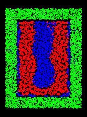

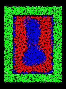
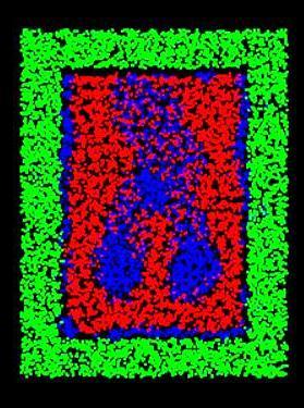

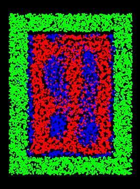


36 Example of DPD Simulation Top-down PS-b-PMMA Top Sidewall Bottom X-section 36
37 Metrology for DSA 3D Profile Tool TEM XSEM AFM CD-SAXS OCD Method Imaging tool Diffraction tool (image is derived from computation) Application Resolution Resolution Nondestructive Non-destructive Frequency analysis Simple model Non-destructive Monitor internal structure High throughput Concerns Destructive Sample damage Destructive Sample damage Only surface topography Resolution Only surface topography Target size Model complexity TEM, XSEM and SAXS are required for DSA material development. OCD is effective for process window analysis and SPC/APC 37
38 Challenges for DSA Lithography High performance DSA material Resolution LWR/LER Etching Long term stability Robust material and tool for environmental control such as surface energy stability, temperature, humidity, pressure and PH, etc. Defectivity, CD and overlay accuracy Development of molecular dynamics based DSA simulator More accurate simulation model BCP and related molecular design Microphase separation (2D/3D) DSA and guide patterning (litho/wet/dry) TAT vs accuracy trade-off DSA OPC/DFM technology Design rule verification Metrology & Inspection Metrology for 3D profile Inspection technology for 1xnmhp and beyond needs to overcome t-put vs accuracy/sensitivity trade-off. 38
39 Half pitch [nm] Key Challenges for Shrinking 40 Immersion SADP DRAM metal MPU metal Flash gate SAQP/SAOP?/EUVL /NIL/+DSA/ Year of production? Metrology & Inspection technologies should be prepared for NGL? 39
40 Contents Device Roadmap and Lithography Extendibility toward 1x nm hp and beyond with New Lithography EUVL NIL DSA Conclusion 40
41 Conclusion EUVL We are waiting EUVL for HV production. Light source performance is a significant concern. NIL NIL performance has been improving as alternative lithography for next generation devises to reduce process cost as well as pattern size. DSA DSA will be a complementary technology for all other lithography Next Challenges Single exposure NIL will be enabled by mask(template) technology revolution. Next generation lithography will depend on innovation of infrastructure technologies such as OPC, DFM, M&I, etching and cleaning. 41
42 2013/6/13 42
NIL defect performance toward High volume mass production
 NIL defect performance toward High volume mass production Masayuki Hatano a, Kei Kobayashi a, Hiroyuki Kashiwagi a, Hiroshi Tokue a, Takuya Kono a, Nakasugi Tetsuro a, Eun Hyuk Choi b, Wooyung Jung b a
Integration of Block-Copolymer with Nano- Imprint Lithography: Pushing the Boundaries of Emerging Nano-Patterning Technology
 Integration of Block-Copolymer with Nano- Imprint Lithography: Pushing the Boundaries of Emerging Nano-Patterning Technology April 2010 update SNL Geoff Brennecka (PI) Bruce Burckel Matt George Jack Skinner
FIB mask repair technology for EUV mask 1. INTRODUCTION
 FIB mask repair technology for EUV mask Tsuyoshi Amano*, Yasushi Nishiyama*, iroyuki Shigemura*, Tsuneo Terasawa*, Osamu Suga*, Kensuke Shiina**, Fumio Aramaki**, Anto Yasaka** Tsukasa Abe***, iroshi Mohri***
2006 UPDATE METROLOGY
 INTERNATIONAL TECHNOLOGY ROADMAP FOR SEMICONDUCTORS METROLOGY THE ITRS DEVED AND INTENDED FOR TECHNOLOGY ASSESSMENT ONLY AND WITHOUT REGARD TO ANY COMMERCIAL CONSIDERATIONS PERTAINING TO INDIVIDUAL PRODUCTS
THE IMPACT OF 3D DEVICES ON THE FUTURE OF PROCESS MATERIALS TRENDS & OPPORTUNITIES
 THE IMPACT OF 3D DEVICES ON THE FUTURE OF PROCESS MATERIALS TRENDS & OPPORTUNITIES L. Shon Roy K. Holland, PhD. October 2014 Materials Examples Process materials used to make semiconductor devices Gases
Part 3: Test Structures, Test Chips, In-Line Metrology & Inspection
 Part 3: Test Structures, Test Chips, In-Line Metrology & Inspection CTO, Maydan Technology Center Applied Materials, Inc. Mike_Smayling@amat.com Topics Introduction to Test Chips Test Structures Basic
In-Situ Monitoring of Pattern Filling in Nano-Imprint Lithography Using Surface Plasmon Resonance
 Copyright 2011 American Scientific Publishers All rights reserved Printed in the United States of America Journal of Nanoscience and Nanotechnology Vol. 11, 1 6, 2011 In-Situ Monitoring of Pattern Filling
Nanofabrication Prof. Stephen Y. Chou NanoStructure Laboratory
 Nanofabrication Prof. Stephen Y. Chou Department of Electrical Engineering Princeton University 1 Acknowledgment Dr. Paul Fischer Dr. Yun Wang Dr. Jay Guo Dr. Peter Klauss Dr. Jim Wang Dr. Longtin He Dr.
Photolithography I ( Part 2 )
") 1 Photolithography I ( Part 2 ) Chapter 13 : Semiconductor Manufacturing Technology by M. Quirk & J. Serda Bjørn-Ove Fimland, Department of Electronics and Telecommunication, Norwegian University of Science
1 Photolithography I ( Part 2 ) Chapter 13 : Semiconductor Manufacturing Technology by M. Quirk & J. Serda Bjørn-Ove Fimland, Department of Electronics and Telecommunication, Norwegian University of Science
Integrated Process Technology Development for the sub 7nm Era
 Integrated Process Technology Development for the sub 7nm Era July 12, 2017 Alex Oscilowski President TEL Technology Center, America, LLC. TEL s Global R&D Operations Korea U.S. imec (Belgium) TEL Technology
Vertically aligned Ni magnetic nanowires fabricated by diblock-copolymer-directed Al thin film anodization
 Vertically aligned Ni magnetic nanowires fabricated by diblock-copolymer-directed Al thin film anodization Researcher: Kunbae (Kevin) Noh, Graduate Student, MAE Dept. and CMRR Collaborators: Leon Chen,
Next Generation Source Power Requirements. Erik R. Hosler
 Next Generation Source Power Requirements Erik R. Hosler What will we need at the 3 nm node and beyond? Can laser produced plasma sources continue the roadmap? Needs to future EUV manufacturing Lithography
TSV Processing and Wafer Stacking. Kathy Cook and Maggie Zoberbier, 3D Business Development
 TSV Processing and Wafer Stacking Kathy Cook and Maggie Zoberbier, 3D Business Development Outline Why 3D Integration? TSV Process Variations Lithography Process Results Stacking Technology Wafer Bonding
EE40 Lec 22. IC Fabrication Technology. Prof. Nathan Cheung 11/19/2009
 Suggested Reading EE40 Lec 22 IC Fabrication Technology Prof. Nathan Cheung 11/19/2009 300mm Fab Tour http://www-03.ibm.com/technology/manufacturing/technology_tour_300mm_foundry.html Overview of IC Technology
EUV Defect Repair Strategy
 EUV Defect Repair Strategy J.H. Peters, S. Perlitz, U. Matejka, W. Harnisch, D. Hellweg, M. Weiss, M. Waiblinger, T. Bret, T. Hofmann, K. Edinger, K. Kornilov Carl Zeiss SMS / SMT 2011 International Symposium
Laser Produced Plasma for Production EUV Lithography
 TRW / Cutting Edge Optronics Laser Produced Plasma for Production EUV Lithography EUVL Source Workshop October 29, 2001 TRW/CEO Laser-Produced Plasma (LPP) EUV Source Development and Commercialization
Advanced developer-soluble gap-fill materials and applications
 Advanced developer-soluble gap-fill materials and applications Runhui Huang, Dan Sullivan, Anwei Qin, Shannon Brown Brewer Science, Inc., 2401 Brewer Dr., Rolla, MO, USA, 65401 ABSTRACT For the via-first
Micro and nano structuring of carbon based materials for micro injection moulding and hot embossing
 Micro and nano structuring of carbon based materials for micro injection moulding and hot embossing Victor Usov, Graham Cross, Neal O Hara, Declan Scanlan, Sander Paulen, Chris de Ruijter, Daniel Vlasveld,
Novel Spin on Planarization Technology by Photo Curing SOC (P-SOC)
") Journal of Photopolymer Science and Technology Volume 3, Number 3 (17) 373-378 C 17SPST Technical Paper Novel Spin on Planarization Technology by Photo Curing (P-) Takafumi Endo*, Rikimaru Sakamoto, Keisuke
Journal of Photopolymer Science and Technology Volume 3, Number 3 (17) 373-378 C 17SPST Technical Paper Novel Spin on Planarization Technology by Photo Curing (P-) Takafumi Endo*, Rikimaru Sakamoto, Keisuke
From microelectronics down to nanotechnology.
 From microelectronics down to nanotechnology sami.franssila@tkk.fi Contents Lithography: scaling x- and y-dimensions MOS transistor physics Scaling oxide thickness (z-dimension) CNT transistors Conducting
Micro-fabrication and High-productivity Etching System for 65-nm Node and Beyond
 Hitachi Review Vol. 55 (2006), No. 2 83 Micro-fabrication and High-productivity Etching System for 65-nm Node and Beyond Takashi Tsutsumi Masanori Kadotani Go Saito Masahito Mori OVERVIEW: In regard to
TSMC Property. ConFab. Bridging the Fabless-Foundry Gap. BJ Woo. Sr. Director Business Development TSMC TSMC, Ltd
 ConFab Bridging the Fabless-Foundry Gap BJ Woo Sr. Director Business Development TSMC 2 Outline Fabless Requirements Technology Scaling Challenges IP Quality Foundry Integrated Manufacturing Value Summary
Overview of SEMI Standards for EUV Masks. Scott Hector ISMT/Motorola Chairman of SEMI EUV Mask Task Force
 Overview of SEMI Standards for EUV Masks Scott Hector ISMT/Motorola Chairman of SEMI EUV Mask Task Force 1 4 Storage container and attributes of removable protection mechanism (3553) Removable protection
Technology. Semiconductor Manufacturing. Hong Xiao INTRODUCTION TO SECOND EDITION SPIE PRESS
 INTRODUCTION TO Semiconductor Manufacturing Technology SECOND EDITION Hong Xiao TECHNISCHE INFORMATIONSBiBUOTHEK UNIVERSITATSBIBLIOTHEK HANNOVER SPIE PRESS Bellingham,Washington USA Contents Preface to
EUV Mask Image Placement Management in Writing, Registration, and Exposure Tools
 EUV Mask Image Placement Management in Writing, Registration, and Exposure Tools Eric Cotte a *, Uwe Dersch a, Christian Holfeld a, Uwe Mickan b, Holger Seitz c, Thomas Leutbecher c, and Günter Hess c
Proteus. Full-Chip Mask Synthesis. Benefits. Production-Proven Performance and Superior Quality of Results. synopsys.com DATASHEET
 DATASHEET Proteus Full-Chip Mask Synthesis Proteus provides a comprehensive and powerful environment for performing full-chip proximity correction, building models for correction, and analyzing proximity
Lecture 5. SOI Micromachining. SOI MUMPs. SOI Micromachining. Silicon-on-Insulator Microstructures. Agenda:
 EEL6935 Advanced MEMS (Spring 2005) Instructor: Dr. Huikai Xie SOI Micromachining Agenda: SOI Micromachining SOI MUMPs Multi-level structures Lecture 5 Silicon-on-Insulator Microstructures Single-crystal
Filtration on block copolymer solution used in directed self assembly lithography
 Filtration on block copolymer solution used in directed self assembly lithography Toru Umeda*, Tomoyuki Takakura and Shuichi Tsuzuki Nihon Pall Ltd., 46 Kasuminosato, Ami-machi, Inashiki-gun, Ibaraki,
EXCIMER LASER ANNEALING FOR LOW- TEMPERATURE POLYSILICON THIN FILM TRANSISTOR FABRICATION ON PLASTIC SUBSTRATES
 EXCIMER LASER ANNEALING FOR LOW- TEMPERATURE POLYSILICON THIN FILM TRANSISTOR FABRICATION ON PLASTIC SUBSTRATES G. Fortunato, A. Pecora, L. Maiolo, M. Cuscunà, D. Simeone, A. Minotti, and L. Mariucci CNR-IMM,
Step and Flash Imprint Lithography for sub-100nm Patterning
 Step and Flash Imprint Lithography for sub-100nm Patterning Matthew Colburn, Annette Grot, Marie Amistoso, Byung Jin Choi, Todd Bailey, John Ekerdt, S.V. Sreenivasan, James Hollenhorst, C. Grant Willson
Customer Support: Leveraging Value of Ownership
 Customer Support: Leveraging Value of Ownership Bernard Carayon SVP Customer Support WW Analyst Day, 30 September 2004 / Slide 1 Agenda! Customer Support main activities! Worldwide Organization and installed
Electron Beam Lithography - key enabling technology in nanofabrication. Frank Dirne
 Electron Beam Lithography - key enabling technology in nanofabrication Frank Dirne Moore s Law (x2/2 yr) Moore s Law EBL Electron Beam Lithography - key enabling technology in nanofabrication - Principles
Surface Preparation and Cleaning Conference April 19-20, 2016, Santa Clara, CA, USA. Nano-Bio Electronic Materials and Processing Lab.
 Surface Preparation and Cleaning Conference April 19-20, 2016, Santa Clara, CA, USA Issues on contaminants on EUV mask Particle removal on EUV mask surface Carbon contamination removal on EUV mask surface
High Temperature Oxygen Out-Diffusion from the Interfacial SiOx Bond Layer in Direct Silicon Bonded (DSB) Substrates
 Substrates") High Temperature Oxygen Out-Diffusion from the Interfacial SiOx Bond Layer in Direct Silicon Bonded (DSB) Substrates Jim Sullivan, Harry R. Kirk, Sien Kang, Philip J. Ong, and Francois J. Henley Silicon
High Temperature Oxygen Out-Diffusion from the Interfacial SiOx Bond Layer in Direct Silicon Bonded (DSB) Substrates Jim Sullivan, Harry R. Kirk, Sien Kang, Philip J. Ong, and Francois J. Henley Silicon
Measurement of thickness of native silicon dioxide with a scanning electron microscope
 Measurement of thickness of native silicon dioxide with a scanning electron microscope V. P. Gavrilenko* a, Yu. A. Novikov b, A. V. Rakov b, P. A. Todua a a Center for Surface and Vacuum Research, 40 Novatorov
MCC. PMGI Resists NANO PMGI RESISTS OFFER RANGE OF PRODUCTS
 MCC PMGI RESISTS OFFER Sub.25µm lift-off processing Film thicknesses from 5µm Choice of resin blends for optimal undercut control High thermal stability Superior adhesion to Si, NiFe, GaAs, InP
Hybrid BARC approaches for FEOL and BEOL integration
 Hybrid BARC approaches for FEOL and BEOL integration Willie Perez a, Stephen Turner a, Nick Brakensiek a, Lynne Mills b, Larry Wilson b, Paul Popa b a Brewer Science, Inc., 241 Brewer Dr., Rolla, MO 6541
Large-area patterning by roller-based nanoimprint lithography
 JOANNEUM RESEARCH Forschungsgesellschaft Institute MATERIALS, Weiz, Austria Large-area patterning by roller-based nanoimprint lithography Ursula Palfinger, Dieter Nees, Stephan Ruttloff, Markus Leitgeb,
Semicon Europa Wafer Chucks for Lithography. Berliner Glas KGaA Herbert Kubatz GmbH & Co. Sven Götze
 Semicon Europa 2011. Wafer Chucks for Lithography. Berliner Glas KGaA Herbert Kubatz GmbH & Co. Sven Götze 1 Export driven, medium-sized, innovative. Solutions in Optics High Tech in Glass Legal form:
Process Flow in Cross Sections
 Process Flow in Cross Sections Process (simplified) 0. Clean wafer in nasty acids (HF, HNO 3, H 2 SO 4,...) --> wear gloves! 1. Grow 500 nm of SiO 2 (by putting the wafer in a furnace with O 2 2. Coat
PARAMETER EFFECTS FOR THE GROWTH OF THIN POROUS ANODIC ALUMINUM OXIDES
 10.1149/1.2794473, The Electrochemical Society PARAMETER EFFECTS FOR THE GROWTH OF THIN POROUS ANODIC ALUMINUM OXIDES S. Yim a, C. Bonhôte b, J. Lille b, and T. Wu b a Dept. of Chem. and Mat. Engr., San
The Effects of Defects on the Moisture-Barrier Performance of Clear Coatings on Polymer Substrates.
 AIMCAL, CHARLESTON, SC, 2013 The Effects of Defects on the Moisture-Barrier Performance of Clear Coatings on Polymer Substrates. The National Centre for Printed Electronics ALF part SMITH of Centre for
Semiconductor Manufacturing Technology. IC Fabrication Process Overview
 Semiconductor Manufacturing Technology Michael Quirk & Julian Serda October 00 by Prentice Hall Chapter 9 IC Fabrication Process Overview /4 Objectives After studying the material in this chapter, you
Post CMP Cleaning SPCC2017 March 27, 2017 Jin-Goo Park
 Post CMP Cleaning Conference @ SPCC2017 March 27, 2017 Jin-Goo Park Challenges in surface preparation Research trend in cleaning technology Lesson learned from current cleaning technology Challenges in
Enabling Technology in Thin Wafer Dicing
 Enabling Technology in Thin Wafer Dicing Jeroen van Borkulo, Rogier Evertsen, Rene Hendriks, ALSI, platinawerf 2G, 6641TL Beuningen Netherlands Abstract Driven by IC packaging and performance requirements,
Multiphoton lithography based 3D micro/nano printing Dr Qin Hu
 Multiphoton lithography based 3D micro/nano printing Dr Qin Hu EPSRC Centre for Innovative Manufacturing in Additive Manufacturing University of Nottingham Multiphoton lithography Also known as direct
LOT. Contents. Introduction to Thin Film Technology. Chair of Surface and Materials Technology
 Introduction to Thin Film Contents 1. Introduction and Application Examples (2h) 2. Preparation of Thin Films by PVD (Physical Vapor Deposition) (6h) 2.1 Vacuum Technique (1h) 2.1.1 Kinetics of Gases 2.1.2
Solvent pre-wetting as an effective start-up method for point-of-use filter
 Solvent pre-wetting as an effective start-up method for point-of-use filter Toru Umeda* a, Shinichi Sugiyama, Takashi Nakamura, Makoto Momota b, Michael Sevegney c, Shuichi Tsuzuki, Toru Numaguchi a a
Technical Data Sheet Technisches Datenblatt
 AZ ECI 3000 Photoresist Universal i-line/crossover Photoresist Series GENERAL INFORMATION AZ ECI 3000 photoresist series are a family of fast positive resists with high resolution capabilities (0.4 µm
MCC. NANO PMMA and Copolymer
 MCC PRODUCT ATTRIBUTES NANO and Submicron linewidth control (polymethyl methacrylate) is a versatile polymeric material that is well suited Sub 0.1µm imaging for many imaging and non-imaging microelectronic
Metallization deposition and etching. Material mainly taken from Campbell, UCCS
 Metallization deposition and etching Material mainly taken from Campbell, UCCS Application Metallization is back-end processing Metals used are aluminum and copper Mainly involves deposition and etching,
SUSS SOLUTIONS FOR LARGE FORMAT PATTERNING UV Scanning Lithography and Excimer Laser Ablation
 SUSS SOLUTIONS FOR LARGE FORMAT PATTERNING UV Scanning Lithography and Excimer Laser Ablation Kevin Yang, Habib Hichri, Ralph Zoberbier SÜSS MicroTec Photonic Systems Inc. June 18, 2015 MARKET DRIVER Mobile
MICROFABRICATION OF OPTICALLY ACTIVE InO X MICROSTRUCTURES BY ULTRASHORT LASER PULSES
 Journal of Optoelectronics and Advanced Materials Vol. 4, No. 3, September 2002, p. 809-812 MICROFABRICATION OF OPTICALLY ACTIVE InO X MICROSTRUCTURES BY ULTRASHORT LASER PULSES Foundation for Research
Nanoimprint Lithography - Next Generation Nanopatterning Methods for Nanophotonics Fabrication
 14 Nanoimprint Lithography - Next Generation Nanopatterning Methods for Nanophotonics Fabrication Jukka Viheriälä, Tapio Niemi, Juha Kontio and Markus Pessa Optoelectronics Research Centre, Tampere University
Multilayer Development for Extreme Ultraviolet and Shorter Wavelength Lithography
 Multilayer Development for Extreme Ultraviolet and Shorter Wavelength Lithography Eric Louis 1, Igor Makhotkin 1, Erwin Zoethout 1, Stephan Müllender 2 and Fred Bijkerk 1,3 1 FOM Institute for Plasma Physics
Thin Wafers Bonding & Processing
 Thin Wafers Bonding & Processing A market perspective 2012 Why New Handling Technologies Consumer electronics is today a big driver for smaller, higher performing & lower cost device configurations. These
Materials Characterization for Stress Management
 Materials Characterization for Stress Management Ehrenfried Zschech, Fraunhofer IZFP Dresden, Germany Workshop on Stress Management for 3D ICs using TSVs San Francisco/CA, July 13, 2010 Outline Stress
Simulation Analysis of Defect Repair Methods for EUVL Mask Blanks
 Simulation Analysis of Defect Repair Methods for EUVL Mask Blanks Association of Super-Advanced Electronics Technologies (ASET) EUV Process Technology Research Laboratory Takeo Hashimoto and Iao Nishiyama
Photoresist Coat, Expose and Develop Laboratory Dr. Lynn Fuller
 ROCHESTER INSTITUTE OF TECHNOLOGY MICROELECTRONIC ENGINEERING Photoresist Coat, Expose and Develop Laboratory Dr. Lynn Fuller Webpage: http://www.rit.edu/lffeee 82 Lomb Memorial Drive Rochester, NY 14623-5604
If it moves, chop it in half, then simulate it
 Interactions of Double Patterning Technology with wafer processing, OPC and design flows Kevin Lucas, Chris Cork, Alex Miloslavsky, Gerry Luk-Pat, Levi Barnes, John Hapli, John Lewellen, Greg Rollins Synopsys
Processing guidelines
 Processing guidelines mr-uvcur21 series UV-curable Polymer for UV-based Nanoimprint Lithography Characteristics mr-uvcur21 is a liquid UV-curable polymer system with low viscosity and high curing rate
Lecture 19 Microfabrication 4/1/03 Prof. Andy Neureuther
 EECS 40 Spring 2003 Lecture 19 Microfabrication 4/1/03 Prof. ndy Neureuther How are Integrated Circuits made? Silicon wafers Oxide formation by growth or deposition Other films Pattern transfer by lithography
FY06 ACCOMPLISHMENTS. Nanoelectronics Manufacture, Inspection, and Repair using Thermal Dip Pen Nanolithography
 FY06 ACCOMPLISHMENTS Nanoelectronics Manufacture, Inspection, and Repair using Thermal Dip Pen Nanolithography William P. King Georiga Institute of Technology FY06 was the second year of this grant, and
Chips Face-up Panelization Approach For Fan-out Packaging
 Chips Face-up Panelization Approach For Fan-out Packaging Oct. 15, 2015 B. Rogers, D. Sanchez, C. Bishop, C. Sandstrom, C. Scanlan, TOlson T. REV A Background on FOWLP Fan-Out Wafer Level Packaging o Chips
IMPLEMENTATION OF A FULLY MOLDED FAN-OUT PACKAGING TECHNOLOGY
 IMPLEMENTATION OF A FULLY MOLDED FAN-OUT PACKAGING TECHNOLOGY B. Rogers, C. Scanlan, and T. Olson Deca Technologies, Inc. Tempe, AZ USA boyd.rogers@decatechnologies.com ABSTRACT Fan-Out Wafer-Level Packaging
EUVL Mask Defect Strategy
 EUVL Mask Defect Strategy EUV Mask March 4, 2002, Santa Clara, CA Alan Stivers, Ted Liang, Barry Lieberman, Pei-yang Yan, Fu-Chang Lo Intel Corporation, Santa Clara, CA USA Outline Introduction Overall
Self Assembled Heterojunction Solar Cell Active Layers: CFN/USB/CAT Collaboation
 Self Assembled Heterojunction Solar Cell Active Layers: CFN/USB/CAT Collaboation Supported in part by the SensorCat program at NYSTAR,NSF-MRSEC Jennifer A. Segui PhD student in Biomedical Engineering.
Laser Spike Annealing for sub-20nm Logic Devices
 Laser Spike Annealing for sub-20nm Logic Devices Jeff Hebb, Ph.D. July 10, 2014 1 NCCAVS Junction Technology Group Semicon West Meeting July 10, 2014 Outline Introduction Pattern Loading Effects LSA Applications
VLSI Technology. By: Ajay Kumar Gautam
 By: Ajay Kumar Gautam Introduction to VLSI Technology, Crystal Growth, Oxidation, Epitaxial Process, Diffusion Process, Ion Implantation, Lithography, Etching, Metallization, VLSI Process Integration,
Precise Ion and Electron Beam Processing for Nano-Structuring
 Precise Ion and Electron Beam Processing for Nano-Structuring Regina Korntner, Hans Loeschner and Elmar Platzgummer Vienna, Austria 1 Outline Short Introduction to IMS Technology Introduction History of
EV Group 300mm Wafer Bonding Technology July 16, 2008
 EV Group 300mm Wafer Bonding Technology July 16, 2008 EV Group in a Nutshell st Our philosophy Our mission in serving next generation application in semiconductor technology Equipment supplier for the
Fabrication of aligned metallic structures based on block copolymer lithography
 88 Fabrication of aligned metallic structures based on block copolymer lithography Yusuke Takahashi Department ofmicroelectronic Engineering, Rochester Institute of Technology, 82 Lomb Memorial Dr., Rochester,
Ultra High Barrier Coatings by PECVD
 Society of Vacuum Coaters 2014 Technical Conference Presentation Ultra High Barrier Coatings by PECVD John Madocks & Phong Ngo, General Plasma Inc., 546 E. 25 th Street, Tucson, Arizona, USA Abstract Silicon
Laser Micromachining for Industrial Applications and R&D. 3D-Micromac AG. Symposium on Smart Integrated Systems in Chemnitz. 3D-Micromac AG
 3D-Micromac AG Symposium on Smart Integrated Systems in Chemnitz 1 1 microdice - TLS-Dicing for separation of SiC 2 microprep - for high-throughput microstructure diagnostics 3 About 3D-Micromac AG 2 microdice
UV5 POSITIVE DUV PHOTORESIST For Microlithography Applications
 UV5 POSITIVE DUV PHOTORESIST For Microlithography Applications DESCRIPTION UV5 positive DUV photoresist has been optimized to provide vertical profile imaging of isolated and semidense features for device
New Materials as an enabler for Advanced Chip Manufacturing
 New Materials as an enabler for Advanced Chip Manufacturing Drive Innovation, Deliver Excellence ASM International Analyst and Investor Technology Seminar Semicon West July 10 2013 Outline New Materials:
Copyright. Stephen Christopher Johnson
 Copyright by Stephen Christopher Johnson 2005 The Dissertation Committee for Stephen Christopher Johnson Certifies that this is the approved version of the following dissertation: Step and Flash Imprint
Amorphous Oxide Transistor Electrokinetic Reflective Display on Flexible Glass
 Amorphous Oxide Transistor Electrokinetic Reflective Display on Flexible Glass Devin A. Mourey, Randy L. Hoffman, Sean M. Garner *, Arliena Holm, Brad Benson, Gregg Combs, James E. Abbott, Xinghua Li*,
FABRICATION AND RELIABILITY OF ULTRA-FINE RDL STRUCTURES IN ADVANCED PACKAGING BY EXCIMER LASER ABLATION
 FABRICATION AND RELIABILITY OF ULTRA-FINE RDL STRUCTURES IN ADVANCED PACKAGING BY EXCIMER LASER ABLATION NCCAVS Joint Users Group Technical Symposium San Jose, June 7 th, 2017 Markus Arendt, SÜSS MicroTec
FOR SEMICONDUCTORS 2005 EDITION
 INTERNATIONAL TECHNOLOGY ROADMAP FOR SEMICONDUCTORS 2005 EDITION YIELD ENHANCEMENT THE ITRS IS DEVISED AND INTENDED FOR TECHNOLOGY ASSESSMENT ONLY AND IS WITHOUT REGARD TO ANY COMMERCIAL CONSIDERATIONS
Novel Solutions for ESD Sensitive Devices
 Novel Solutions for ESD Sensitive Devices Chris Schreiber Magnecomp cschreiber@magnecomp.com Safely Dissipating ESD Problem Static Charging is created by either Tribocharging or Induction and the uncontrolled
Electron Beam Induced Processes and their Applicability to Mask Repair
 & Electron Beam Induced Processes and their Applicability to Mask Repair Hans W.P. Koops (1), Volker Boegli (1), Klaus Edinger (1), Johannes Bihr (2), Jens Greiser (2), (1) NaWoTec GmbH Rossdorf Germany
MARORA A Plasma Selective-oxidation Apparatus for Metal-gate Devices
 Hitachi Review Vol. 57 (2008), No. 3 127 MARORA A Plasma Selective-oxidation Apparatus for Metal-gate Devices Tadashi Terasaki Masayuki Tomita Katsuhiko Yamamoto Unryu Ogawa, Dr. Eng. Yoshiki Yonamoto,
ULTRA-SMALL VIA-TECHNOLOGY OF THINFILM POLYMERS USING ADVANCED SCANNING LASER ABLATION
 ULTRA-SMALL VIA-TECHNOLOGY OF THINFILM POLYMERS USING ADVANCED SCANNING LASER ABLATION Michael Töpper Fraunhofer Research Institution for Reliability and Microintegration IZM Germany Martin Wilke, Klaus-Dieter
Via Fill in Small Trenches using Hot Aluminum Process. By Alice Wong
 Via Fill in Small Trenches using Hot Aluminum Process By Alice Wong Goals for Project Good Via Fill in Small contact holes using hot aluminum process Be able to get good images of the contact holes using
Visit
 Practical Applications for Nano- Electronics by Vimal Gopee E-mail: Vimal.gopee@npl.co.uk 10/10/12 Your Delegate Webinar Control Panel Open and close your panel Full screen view Raise hand for Q&A at the
Ajay Kumar Gautam [VLSI TECHNOLOGY] VLSI Technology for 3RD Year ECE/EEE Uttarakhand Technical University
![Ajay Kumar Gautam [VLSI TECHNOLOGY] VLSI Technology for 3RD Year ECE/EEE Uttarakhand Technical University](/thumbs/75/72824557.jpg "Ajay Kumar Gautam [VLSI TECHNOLOGY] VLSI Technology for 3RD Year ECE/EEE Uttarakhand Technical University") 2014 Ajay Kumar Gautam [VLSI TECHNOLOGY] VLSI Technology for 3RD Year ECE/EEE Uttarakhand Technical University Page1 Syllabus UNIT 1 Introduction to VLSI Technology: Classification of ICs, Scale of integration,
2014 Ajay Kumar Gautam [VLSI TECHNOLOGY] VLSI Technology for 3RD Year ECE/EEE Uttarakhand Technical University Page1 Syllabus UNIT 1 Introduction to VLSI Technology: Classification of ICs, Scale of integration,
ZERO DEFECTS Entegris Newsletter
 July 215 CONTENTS 1. Entegris News Entegris Reaches Milestones at its i2m Center for Advanced Materials Science Entegris @ SEMICON West 2. Process Stability InVue CR288 Concentration Monitor Application
Lecture 6. Through-Wafer Interconnect. Agenda: Through-wafer Interconnect Polymer MEMS. Through-Wafer Interconnect -1. Through-Wafer Interconnect -2
 Agenda: EEL6935 Advanced MEMS (Spring 2005) Instructor: Dr. Huikai Xie Lecture 6 Through-wafer Interconnect EEL6935 Advanced MEMS 2005 H. Xie 1/21/2005 1 Motivations: Wafer-level packaging CMOS 3D Integration
THIN FILM THICKNESS MEASUREMENT FOR EVALUATION OF RESIDUAL LAYER OF NANO-IMPRINT LITHOGRAPHY USING NEAR-FIELD OPTICS
 9 th INTERNATIONAL SYMPOSIUM ON MEASUREMENT AND QUALITY CONTROL (9 th ISMQC) November 21 24, 27, IIT Madras THIN FILM THICKNESS MEASUREMENT FOR EVALUATION OF RESIDUAL LAYER OF NANO-IMPRINT LITHOGRAPHY
Resist Characterization for EUV- Lithography
 Resist Characterization for EUV- Lithography 2. Int. EUVL-Symposium, Antwerp, B Wolf-Dieter Domke 1, Stefan Hirscher 2, liver Kirch 3, Karl Kragler 1, Klaus Lowack 1, 1 Infineon Technologies AG, 91050
Modeling of Local Oxidation Processes
 Introduction Isolation Processes in the VLSI Technology Main Aspects of LOCOS simulation Athena Oxidation Models Several Examples of LOCOS structures Calibration of LOCOS effects using VWF Field Oxide
Modeling for DFM / DFY
 Modeling for DFM / DFY A Foundry Perspective Walter Ng Senior Director, Platform Alliances 5/24/07 2006 Chartered Semiconductor Manufacturing Ltd. All rights reserved. No part or parts hereof may be reproduced,
CMOS Manufacturing process. Circuit designer. Design rule set. Process engineer. Set of optical masks. Fabrication process.
 CMOS Manufacturing process Circuit design Set of optical masks Fabrication process Circuit designer Design rule set Process engineer All material: Chap. 2 of J. Rabaey, A. Chandrakasan, B. Nikolic, Digital
Device and Process Variability
 IEEE SCV-SF Electron Devices Society Seminar Device and Process Variability Tomasz Brozek PDF Solutions Inc.. Santa Clara, 12 June 2017 Outline Why does it matter Impact on parametric yield, speed, leakage
Optical Profilometry of Substrate Bow Reduction Using Temporary Adhesives
 Optical Profilometry of Substrate Bow Reduction Using Temporary Adhesives a Paul Flynn and b John Moore a FRT of America, LLC 1101 South Winchester Blvd., Suite L-240, San Jose, CA 95128 408-261-2632,
Figure 2.3 (cont., p. 60) (e) Block diagram of Pentium 4 processor with 42 million transistors (2000). [Courtesy Intel Corporation.
 (e) Block diagram of Pentium 4 processor with 42 million transistors (2000). [Courtesy Intel Corporation.") Figure 2.1 (p. 58) Basic fabrication steps in the silicon planar process: (a) oxide formation, (b) selective oxide removal, (c) deposition of dopant atoms on wafer, (d) diffusion of dopant atoms into exposed
Figure 2.1 (p. 58) Basic fabrication steps in the silicon planar process: (a) oxide formation, (b) selective oxide removal, (c) deposition of dopant atoms on wafer, (d) diffusion of dopant atoms into exposed
Total Cost of Operations TCO
 Total Cost of Operations TCO Agenda Introduction Objectives Elements of TCO ABC Costing TCO in a working Fab Fab Cost Product Margin Building TCO Model Summary Introduction Total Cost of Operations is
Optimizing spray coater process parameters
 Optimizing spray coater process parameters Dr. Eleonora Storace, Florian Palitschka, Dr. Dietrich Tönnies SUSS MicroTec Lithography GmbH Germany Published in the SUSS report 01/2014 E-mail: info@suss.com