Welcome to Streamline Circuits Lunch & Learn. Design for Reliability & Cost Reduction of Advanced Rigid-Flex/Flex PCB Technology
|
|
|
- Primrose Franklin
- 6 years ago
- Views:
Transcription
1
2
3 Welcome to Streamline Circuits Lunch & Learn Design for Reliability & Cost Reduction of Advanced Rigid-Flex/Flex PCB Technology
4 Accurate PCB data is critical to the tooling process. Here are some key items that you should always include when ordering PCB s
5 Fabrication drawing that lists the overall & critical dimensions of the PCB graphically. Drawing should also illustrate the layer stack up detail with overall thickness and any critical thicknesses between layers. All other critical information such as Solder Mask color, Silk Screen color, & Final Finish should also be included in your drawing. Indicate on drawing to build per IPC Standards and list the Class & type that best meets your needs. Most PCB S used in consumer products are built to Class II, and most Military, Aerospace, and Medical requiring high reliability will either require Class III or IIIA.
6 As you all may be are aware, our industry has many data formats with Gerber (RS274X or D) being the most commonly used. However most PCB fabricators prefer the ODB++ format, including Streamline Circuits for it s built in intelligence.
7 Technology Factors that influence the PCB cost. Material type Layer count Number of lamination cycles Number of drill cycles Lines & Spaces under 3.5 and some fabricators 5 mils will drive cost. Via fill per IPC 4761 Type 6 or 7 Final finish specifications Tolerances required exceed IPC Turn time PCB size Batch size Class type
8 When High Reliability PCB S are needed Specify Class III plating in the holes. This will increase the amount of copper in the holes by 20% vs. Class II. Add tear drops at all trace to pad junctures for added land area. Via fill your vias per IPC 4761 type 6 or 7 for the best possible via protection. Require your fabricator to show you that they meet or exceed your requirements by providing cross sections & test reports.
9 When High Reliability PCB S are needed Is there a risk that advice provided can actually increase the price of the PCB? In some cases, yes, especially at the prototype stage where perhaps more attention needs to be focused on lowest total cost for when that product is to be produced in volume, and the real benefits of lowest cost is most important.


10 Design Strategies Epoxy fill with copper Vias Resin Fill off set Vias Resin fill/stacked Vias All Copper Fill process
11 HDI Technology

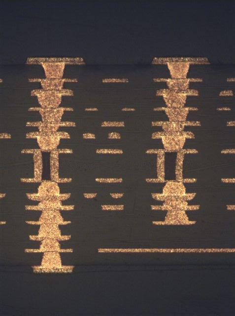
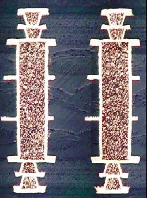
12 What type of via hole plugging is recommended? The preferred type of plugging for standard product is IPC 4761 type VI filled and covered, with target being complete fill. The image below shows type VI with liquid solder mask coverage. Single sided plugging is not recommended (including type II tented and covered) due to concerns over entrapment of chemistry or likelihood of solder balls being present with HASL finishes.
13 Key Benefits to Via filling Improved reliability by reducing the risk of trapped air or liquids. Tighter BGA pitches and higher density interconnects by allowing for via-in-pad instead of dog bone designs. Streamline Circuits can support.25mm BGA requirements. Reliable filled and stacked via constructions. Planar copper surfaces above filled via for more reliable surface mounts and increased assembly yields. Enhanced thermal dissipation.
14 Design Advise Copper thickness of each layer and what is really needed. As a good rule of thumb, the lines and spaces should be a minimum 5x the copper base thickness. Example if you require 1oz finish on outer layers the lines & spaces should be a minimum 3.5 mils. Inner layers can use a multiply of 4.5x if not going through any additional plating processes.
15 Key factors in specifying materials CTE Z axis (Co-efficient of thermal expansion): This is a measure of how much the base material will expand when heated. Td (Decomposition temperature): This is the temperature at which material weight changes by 5%. This parameter determines the thermal survivability of the material. Tg (Glass transition temperature): The temperature at which the material stops acting like a rigid material and begins to behave like a plastic / softer. T260 (Time to delamination): This is the time it take for the base material to delaminate when subjected to a temperature of 260 degrees C. T288 (Time to delamination): This is the time it take for the base material to delaminate when subjected to a temperature of 288 degrees C. Dk (Dielectric constant): The ratio of the capacitance using that material as a dielectric, compared to a similar capacitor which has a vacuum as its dielectric. CTI (Comparative tracking Index): A measure of the electrical breakdown properties of an insulating material. It is used for electrical safety assessment of electrical apparatus.


16 Flex & Rigid Flex Tips Don t suddenly change track widths Don t do this Do this instead

17 Flex & Rigid Flex Tips Added support for pads

18 Flex & Rigid Flex Tips Cover lay openings should be smaller than the pad width in order to help anchor down the pads.

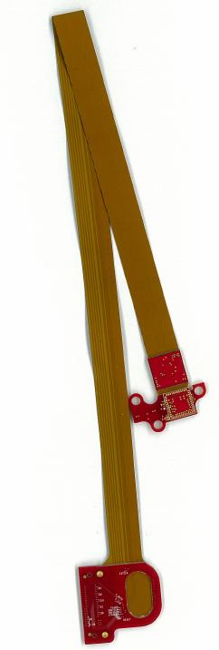
19 Flex & Rigid Flex Tips Transition Zone from Rigid Area to Flexible Area.

20 Flex & Rigid Flex Tips Should always have a minimum 50 mil clearances from any features in Transition Zone.
21 Flex & Rigid Flex Tips Nearly all Flex and Rigid-Flex boards are constructed with polyimide inside and this material is highly hydroscopic. It is strongly recommended to bake the boards to reduce the amount of moisture inside the boards before any type of soldering operation. Without such baking there is risk of delaminating, inner-layer separation or cracking of the hole walls.
22 Flex & Rigid Flex Tips Recommendation for baking per IPC-TM-650 Conditioning The test specimen shall be conditioned by drying in an oven to remove moisture for a minimum of six (6) hours at 105 to 125 C [221 to 257 F]. This conditioning process is mandatory if this method is used for qualification purposes. This method shall replicate the assembly process. The requirement for conditioning (bake/drying) shall be in accordance with product/process lot acceptance criteria. If conditioning of the PCB is not part of the normal assembly process, and this method is being used for acceptance testing, then conditioning is not a requirement Test specimens that are thicker or more complex may require longer baking times to achieve acceptable moisture levels. Record the bake times and temperature if different than those stated in (see 6.2).


23 RIGID-FLEX EXAMPLES 6 Layer Rigid Flex 8 Layer Rigid Flex Microvia 6 Layer Rigid Flex with Cavity 10 Layer Rigid Flex Microvia BGA 10 Layer Rigid Flex with Cavity and 4 flex, Microvia, Buried and Blind vias
24 MANUFACTURING CAPABILITIES STANDARD ADVANCED SINGLE-SIDE FLEXIBLE PANEL SIZE 12"x18" 18"x24" 20"x26" 24"x36" DOUBLE-SIDE FLEXIBLE PANEL SIZE 12"x18" 18"x24" and Up MULTILAYER FLEX PANEL SIZE 12"x18" 18"x24" and Up Layer Count 3 to RIGID FLEX PANEL SIZE 12"x18" 18"x24" and Up Layer Count 2 to Multiple Lamination Copper Foil Weights Internal/ External Kapton Polyimide Stiffener FR4 Stiffener Polyimide Rigid Stiffener 1/4 to 2 ounce Up to 3 ounce.001" to..008" and 007" Up.003" to. 062".063" and Up.003" to. 062".063" and Up Lines, spaces & pad diameters Internal Line Width.0035".001" Internal Spacing.0035".001" External Line Width.0035".001" External Spacing.0035".001" SMT Pitch.010".010" Controlled Impedance 10% 5% Via hole Finish STANDARD ADVANCED Laser Micro Vias.004".002" Blind/buried Vias.004".002" Laser Pads.004".002" Minimum Drilled Hole Size.012".0079" Drilled Hole to Copper.008".007" Castellation Yes Yes Finish surface Tin Lead Plating Thickness.0003" to. 0005" Less.0005" Tin Nickel Plating Thickness 150 Micro Inches 250 Micro Inches Low Stress Nickel 100 Micro Inches 250 Micro Inches Gold Plating Thickness 30 Micro Inches As Specified Electroless Nickel/Immersion Gold Yes Yes Immersion Gold Yes Yes Immersion Silver Yes Yes Entek 106A HT Yes Yes HASL Yes Yes TOLERANCES Plated Hole Tolerances (+/-).002".001" Non-Plated Hole Tolerances (+/-).001".001" Fabrication Tolerance (+/-).005".003" Vision Rout (+/-).003".002" Laser Rout (+/-).002".001"
 FLEX SINGLE-SIDE CIRCUIT CONSTRUCTION SINGLE-SIDED FEATURES: -Very thin construction.003 -.")
 -One conductive layer -Reverse bared or back bared pads, provide access from both sides of the part -Support &")


25 SINGLE-SIDE FLEXIBLE CIRCUITS Single-Side flexible circuits consist of a single conductive layer on a flexible dielectric film. (see constructions below) FLEX SINGLE-SIDE CIRCUIT CONSTRUCTION SINGLE-SIDED FEATURES: -Very thin construction (.075mm-. 20mm) -One conductive layer -Reverse bared or back bared pads, provide access from both sides of the part -Support & unsupported finger areas WHEN TO USE SINGLE-SIDED FLEX: _ Dynamic flexing applications _ Unusual folding and forming applications _ Installation/service applications / repair _ Limitations on space / thickness _ Installation / service flexing Unsupported Finger SCULPTURED FLEX CIRCUITS Sculptured flex circuits have variable copper thicknesses within the part. Thin copper is used for the flexible regions & thicker copper is used at the interconnection point. Sculptured flex circuits provide bare metal connection & are a highly reliable alternative to mechanically crimped contact pins Supported Finger


26 FLEX DOUBLE-SIDE CIRCUIT CONSTRUCTION DOUBLE-SIDE FLEXIBLE CIRCUITS Double-side flexible circuits consist of two conductive layers & can be with or without platedthrough holes, depending on design requirements (see constructions below) DOUBLE-SIDED FEATURES: WHEN TO USE _ DOUBLE-SIDED FLEX:. Two conductive layers _ Component assembly _ Required when circuit density and layout available on both sides can not be routed on a single layer _ Operating high frequency applications _ Signal or ground / power plane _ Supported and unsupported finger/ applications component areas _ Used for shielding applications _ Dense surface mount assembly _ Controlled impedance applications Adhesive Adhesiveless


27 MULTILAYER FLEX CIRCUIT CONSTRUCTION MULTILAYER FLEX CIRCUITS The construction that have three or more conductor layers are referred to as multilayer flex. The layers of the circuit are interconnected with plated-through holes, and with or without stiffeners. Adhesive MULTILAYER FLEX FEATURES: _ Three or more conductive layers _ Component assembly available on both sides _ Controlled impedance and shielding possible _ Supported and unsupported finger/ component areas WHEN TO USE MULTILAYER FLEX: _ Required when circuit density and layout can not be routed on a single layer or double layer _ Signal or ground / power plane applications _ Increased circuit density _ EMI/RFI shielding _ Used for shielding applications _ Dense surface mount assembly _ Controlled impedance with shielding applications Adhesiveless
.")
. RIGID FLEX FEATURES: _ Two or more conductive layers. _ Combined rigid & flex to achieve high-density packaging. _ Eliminate wires and wire harness assemblies.")

28 RIGID-FLEX CIRCUIT CONSTRUCTION RIGID-FLEX CIRCUIT CONSTRUCTION: Rigid flex circuits are a hybrid construction, consisting of rigid and flexible substrates laminated together into a single package and electrically interconnected by means of plated-through holes with solid flexible or loose leaf flexible construction, and with or without stiffener (see construction below). Rigid flex boards are normally multilayer design, but double-sided (two-metal layer) constructions are possible as well, and in fact, have been selected for certain microelectronic chip-packaging applications. (see constructions below). RIGID FLEX FEATURES: _ Two or more conductive layers. _ Combined rigid & flex to achieve high-density packaging. _ Eliminate wires and wire harness assemblies. _ Folded/bended/positioned into package size. _ Easy assembly and installation. WHEN TO USE RIGID FLEX: _ Required when circuit density and layout can not be routed on a single layer. _ Used when components are mounted on both sides of the rigid and flex section. _ Used to solve high-density packaging problems. _ EMI/RFI shielding. _ Used for shielding applications. _ Dense surface mount assembly. _ Controlled impedance with shielding applications. _ Used to connect rigid boards together. Expose Finger 6 LAYER RIGID FLEX STACKUP 8 LAYER RIGID FLEX WITH UNBONDED STACKUP 6 LAYER RIGID FLEX WITH SILVER SHIELD STACKUP


29 SOLID COPPER: Solid copper is the most common method of shielding. Copper shield can be put on one or both sides of the circuit. Solid copper can also cover selective conductors. Solid copper shields increase the rigidity of the circuit, and should be included in thickness to bend radius ratios. CROSSHATCHED COPPER: Crosshatching is an artwork design that relieves much of the copper shield areas by the use of a pattern. Crosshatch shielding can also cover selective conductor. It also helps the circuit to retain its flexibility and can be put on one or both side. SHIELDING Shielding: If the application requires limits in electromagnetic interference/radiofrequency interference (EMI/RFI) shielding on-board or to fabricate low-voltage circuitry, on rigid or flexible substrates. Shields are material around a conductor or group of conductors that limit these factors. CONDUCTIVE SILVER: Conductive silver can be substituted for the copper for shielding purposes in some applications. Silver can be a solid or crosshatched shield and can be put on one or both sides of the circuit. It can also cover selected conductors only. Silver shielding is not recommended for a dynamic flexing application due to its brittle characteristic, and may be prone to cracking in severe bending applications. MINIMUM EDGE OF SILVER SHIELD: The minimum distance edge of silver epoxy to edge of non common electrical feature of pad / trace coverlay openings exposed pads / traces is and the edge of flex is (See Clearance picture below). Clearance


30 Finish Surface Dielectrics Surface dielectrics are applied to the outside layers of the circuit to insulate the copper conductors. Following are types of surface dielectrics used at all flex. COVERLAY: Coverlay is the layer of insulation film and adhesive that is applied totally or partially over a conductive pattern on the out surfaces of a printed board. This material is normally produced with laser CO2 drill/rout or mechanical drill/rout process. The common via holes are covered with coverlay. The minimum coverlay openings exposed pads for the component holes are. 005 larger than the copper pads. The coverlay openings can be individual barrel pads or gang relief pads depending on area available. LIQUID PHOTOIMAGEABLE SOLDERMASK: Liquid Photoimageable Solder Mask (LPI) is produced by a photo controlled process and used of tight pad spaces. This process enables unique openings to be applied anywhere on the circuit. LPI is usually not used with 2oz copper or above due to the thickness of the copper as it may not conform around the area of some copper features. The via holes are covered with solder mask. The LPI openings expose pads are.003 larger than the copper pads with.003 minimum web spacing. LPI is not recommended for dynamic flex applications.
, the minimum bend radius should be six times the overall thickness and at least.")
 PLATING: The button or barrel plating is a process that allows for the plated")
, the minimum bend radius should be 12 times overall thickness.")
31 Even though flex circuits are very pliable and flexible, there are limits to their flexibility. If the bend radius is too tight, the result can be de-lamination and conductor fracture. Bending and Folding Guidelines BEND RADIUS: For single and double-sided flexible printed wiring boards (PWBs), the minimum bend radius should be six times the overall thickness and at least.050 away from the plated through hole (see diagram below). Example: If the overall thickness of the flex circuits is.012, the minimum bend radius should be.072 RADIUSED TRACES: The radiused traces help to alleviate breading during folding and bending BUTTON OR PADS (BARREL) PLATING: The button or barrel plating is a process that allows for the plated through holes to maintain their connection while the traces are not plated, allowing the circuit to have increased flexibility. For multilayer flexible PWBs and multilayer rigid and flexible PWBs (bonded inner layers), the minimum bend radius should be 12 times overall thickness. Example: If the overall thickness of the flex circuit is.030, the minimum bend radius should be.360 FOLD LINES: The fold lines may be designated by tick marks which may be either in the copper layers or silkscreen layers. These features aid in bending and designating bend location. CIRCUIT TRACE WIDTH: The circuit trace width should not change in bend areas the transition should be at least.030 (.76mm) from the fold line.
,.010 (.25mm) or higher. Can be used to give added rigidity under a component area.")
 STIFFENER: Come in a variety of thickness from.001 (.02mm) up to.007 (.14mm) or higher. Can be used to give added thickness under conductors to meet ZIF connector requirement.")

32 STIFFENERS/PSA STIFFENERS The common stiffeners require support in areas where connectors or other components are applied. Here are the recommended types of guidelines for stiffeners. FR4/POLYIMIDE RIGID STIFFENER: Come in a variety of thicknesses such as.003 (.076mm),.010 (.25mm) or higher. Can be used to give added rigidity under a component area. Can be used as carrier panel for automated assembly processing. Can be bonded to a flex circuit using a pressure sensitive adhesive or a thermoset adhesive. POLYIMIDE (KAPTON) STIFFENER: Come in a variety of thickness from.001 (.02mm) up to.007 (.14mm) or higher. Can be used to give added thickness under conductors to meet ZIF connector requirement. Can be used to give added strength in high wear areas. Can be blanked at the same time as the circuit outline to meet tight tolerance requires. Can be bonded to flex circuits using a pressure sensitive adhesive or a thermoset adhesive AREA OF STIFFENER: The stiffener and coverlay termination points should overlap a minimum of.030 (.76mm) to void stress points. Eliminating stress points reduce the chance of traces breaking and cracking. COMPONENT HOLES: The holed size in the stiffener is recommended.015 (.38mm) minimum larger than the circuit component holes to allow for registration tolerances. PSA: Pressure Sensitive Adhesive is used to bond flex circuits or rigid circuits without heat requirement. The common PSA is used to bond flex circuits to stiffener to support in areas where connectors are applied. PSA also placed in key location to improve circuit placement and mounting.

33 Streamline Circuit s Facility Located in Silicon Valley Manufacturing all levels of technology Time sensitive prototyping through production The facility was established in 1982 New management team installed September ,000 sq ft PCB manufacturing facility Complete manufacturing process under one roof 1 mile from the San Jose Airport Delivery convenience for out of state customers Located in Silicon Valley Short car ride away for pick up & deliveries Financially secure in current market conditions Low cost infrastructure 33
34 Thank you for attending Streamline Circuits Lunch & Learn!
Flexible Printed Circuits Design Guide
 www.tech-etch.com/flex Flexible Printed Circuits Design Guide Multilayer SMT Assembly Selective Plating of Gold & Tin-Lead Fine Line Microvias Cantilevered & Windowed Leads 1 MATERIALS CONDUCTOR Copper
FLEXIBLE & RIGID-FLEX CIRCUITS TECHNICAL ENGINEERING GUIDE. Delivering Quality Since 1952.
 FLEXIBLE & RIGID-FLEX CIRCUITS TECHNICAL ENGINEERING GUIDE Delivering Quality Since 1952. DELIVERING QUALITY SINCE 1952. Epec Engineered Technologies designs and manufactures customized, built-to-print,
Flex and Rigid-Flex Printed Circuit Design
 Flex and Rigid-Flex Printed Circuit Design Old Content - visit altium.com/documentation Modified by on 29-Nov-2016 Related Videos Bending Lines Enhanced Layer Stack Management Layer Stack Regions A rigid-flex
GRAPHIC MANUFACTURING CAPABILITY Q217-18
 All features are design dependent and may not be achievable in combination Reduced Yield / Special values up ( or down ) to the standard limit are design and application dependent Standard features only
Qualification and Performance Specification for Flexible Printed Boards
 Qualification and Performance Specification for Flexible Printed Boards Developed by the Flexible Circuits Performance Specifications Subcommittee (D-12) of the Flexible Circuits Committee (D-10) of IPC
Precision Engineered Parts
 Precision Engineered Parts Photoetching Laser Cutting Forming Finishing Thin Metal Parts Flexible Circuits EMI Shielding Gaskets www.tech-etch.com PHOTOETCHING Tech-Etch specializes in the manufacture
Introduction Conductors. Supply Planes. Dielectric. Vias PCB Manufacturing Process Electronic Assembly Manufacturing Process
 PCBs/Overview Printed Circuit Boards (PCB) Introduction Conductors. Supply Planes. Dielectric. Vias PCB Manufacturing Process Electronic Assembly Manufacturing Process 29/09/2005 EE6471 (KR) 263 PCBs/Overview
ATS Document Cover Page
 221-008 Item Rev Status: RELEASED printed 9/20/2017 2:27:42 PM by Les Deenin ATS: OPERATIN PROCEDURE ATS Document Cover Page Responsible Department: Supply Chain This copy is uncontrolled unless otherwise
IMPACT OF MICROVIA-IN-PAD DESIGN ON VOID FORMATION
 IMPACT OF MICROVIA-IN-PAD DESIGN ON VOID FORMATION Frank Grano, Felix Bruno Huntsville, AL Dana Korf, Eamon O Keeffe San Jose, CA Cheryl Kelley Salem, NH Joint Paper by Sanmina-SCI Corporation EMS, GTS
PCB Production Process HOW TO PRODUCE A PRINTED CIRCUIT BOARD
 NCAB Group Seminars PCB Production Process HOW TO PRODUCE A PRINTED CIRCUIT BOARD NCAB GROUP PCB Production Process Introduction to Multilayer PCBs 2 Introduction to multilayer PCB s What is a multilayer
Optimizing the Insulated Metal Substrate Application with Proper Material Selection and Circuit Fabrication
 Abstract Optimizing the Insulated Metal Substrate Application with Proper Material Selection and Circuit Fabrication Dave Sommervold, Chris Parker, Steve Taylor, Garry Wexler. The Bergquist Company Prescott,
Interconnection Reliability of HDI Printed Wiring Boards
 Presented in the ECWC 10 Conference at IPC Printed Circuits Expo, SMEMA Council APEX and Designers Summit 05 Interconnection Reliability of HDI Printed Wiring Boards Tatsuo Suzuki Nec Toppan Circuit Solutions,
Process & Capability Manual (Vol )
") Process & Capability Manual (Vol. 12-2015) Seite 1 von 13 1 CHAPTER OVERVIEW 1 CHAPTER OVERVIEW... 2 2 MICROCIRTEC A SHORT PROFILE... 3 2.1 WHO WE ARE... 3 2.2 OBJECTIVES & MARKETS... 3 2.3 DECLARATION
Process & Capability Manual (Vol. 12-2015) Seite 1 von 13 1 CHAPTER OVERVIEW 1 CHAPTER OVERVIEW... 2 2 MICROCIRTEC A SHORT PROFILE... 3 2.1 WHO WE ARE... 3 2.2 OBJECTIVES & MARKETS... 3 2.3 DECLARATION
Freescale Semiconductor Tape Ball Grid Array (TBGA) Overview
 Overview") Freescale Semiconductor Tape Ball Grid Array (TBGA) Overview Revision 0 2006 Freescale and the Freescale logo are trademarks of Freescale Semiconductor, Inc. All other product or service names are the
Freescale Semiconductor Tape Ball Grid Array (TBGA) Overview Revision 0 2006 Freescale and the Freescale logo are trademarks of Freescale Semiconductor, Inc. All other product or service names are the
UL PCB Recognition what is it & why do you need to know about it
 UL PCB Recognition what is it & why do you need to know about it Presented by Emma Hudson NCAB Customer Event March 2015 UL and the UL logo are trademarks of UL LLC 2015 Agenda What is UL and what are
14. Designing with FineLine BGA Packages
 14. Designing with FineLine BGA Packages S51014-1.0 Chapter 14, Designing with FineLine BGA Packages, replaces AN 114: Designing with FineLine BGA Packages. Introduction As programmable logic devices (PLDs)
PEC (Printed Electronic Circuit) process for LED interconnection
 process for LED interconnection") PEC (Printed Electronic Circuit) process for LED interconnection Higher wattage LED s/ power components or their placement in higher densities, requires a larger dissipation of heat in a more effective
PEC (Printed Electronic Circuit) process for LED interconnection Higher wattage LED s/ power components or their placement in higher densities, requires a larger dissipation of heat in a more effective
Low CTE / High Tg FR-4 with High Heat Resistance
 Low CTE / High Tg FR-4 with High Heat Resistance Laminate: EM-827 Prepreg: EM-827B 1 Features Tg(DSC) > 170 Z direction CTE < 3.0% (50~260 ) High thermal degradation temperature: Td > 340 Excellent thermal
NCAB Group PCB Specification
 NCAB Group Seminar no. 9 NCAB Group PCB Specification NCAB GROUP NCAB Group PCB Specification 14 key features for durable and reliable PCB s NCAB GROUP NCAB Group PCB Specification 2 Are all PCB s created
10 Manor Parkway, Suite C Salem, New Hampshire
 Micro-Precision Technologies (MPT) is an independent manufacturer of hybrid integrated circuits, multichip modules, and high-precision thick film substrates for the military, medical, avionics, optoelectronics,
Lead Free Assembly: A Practical Tool For Laminate Materials Selection
 Lead Free Assembly: A Practical Tool For Laminate Materials Selection Erik J. Bergum David Humby Isola Abstract: The impending European RoHS legislation, restricting the use of lead containing solders,
TMS320C6000 BGA Manufacturing Considerations
 TMS320C6000 BGA Manufacturing Considerations David Bell C6000 Applications Team Abstract When designing with a high-density BGA package, it is important to be aware of different techniques that aid in
Advances in Printing nano Cu and Using Existing Cu Based Manufacturing Processes. Michael J. Carmody Chief Scientist, Intrinsiq Materials
 Advances in Printing nano Cu and Using Existing Cu Based Manufacturing Processes Michael J. Carmody Chief Scientist, Intrinsiq Materials Why Use Copper? Lower Cost than Silver. Print on Numerous Substrates.
High Frequency Circuit Materials Attributes John Coonrod, Rogers Corporation
 High Frequency Circuit Materials Attributes John Coonrod, Rogers Corporation Specialty high frequency circuit materials have been used in the PCB industry for decades and for many different reasons. There
COFAN USA. Meeting your Project needs.
 COFAN USA Meeting your Project needs www.cofangroup.com PCB Substrate Pre-preg Category SEKISUI Laird T-Clad Denka PCB Substrate Pre-preg Category In the PCB industry, there are a couple major Pre-preg
Welcome to the KEMET Ceramic Capacitor Flex Crack Mitigation product training module. This module will review sources of stress in surface mount
 1 Welcome to the KEMET Ceramic Capacitor Flex Crack Mitigation product training module. This module will review sources of stress in surface mount multilayer ceramic capacitors, provide board layout recommendations,
Images of Failures in Microelectronics Packaging and Assembly
 Images of Failures in Microelectronics Packaging and Assembly Ed Hare, Ph.D./SEM Lab, Inc. IMAPS NW - Feb. 11th 2004 Redmond, WA http://www.semlab.com 1 What is this? http://www.semlab.com 2 Inner Layer
YANTAT PRINTED CIRCUIT (SHENZHEN) CO. LTD.
 CO. LTD.") WWW.YANTAT.COM YANTAT GROUP HK HEAD OFFICE Logistic/Sales YANTAT PRINTED CIRCUIT SHANGHAI SALES OFFICE SHENZHEN SALES OFFICE HONG KONG HEAD OFFICE YANTAT PRINTED CIRCUIT YANTAT PRINTED CIRCUIT YANTAT S
WWW.YANTAT.COM YANTAT GROUP HK HEAD OFFICE Logistic/Sales YANTAT PRINTED CIRCUIT SHANGHAI SALES OFFICE SHENZHEN SALES OFFICE HONG KONG HEAD OFFICE YANTAT PRINTED CIRCUIT YANTAT PRINTED CIRCUIT YANTAT S
3M Electrically Conductive Adhesive Transfer Tape 9707
 Technical Data May 2014 3M Electrically Conductive Adhesive Transfer Tape 9707 Product Description 3M Electrically Conductive Adhesive Transfer Tape (ECATT) 9707 is a pressure sensitive adhesive (PSA)
PERFORMANCE SPECIFICATION PRINTED WIRING BOARD, FLEXIBLE OR RIGID FLEX, GENERAL SPECIFICATION FOR
 The documentation and process conversion measures necessary to comply with this amendment shall be completed by: 6 March 2017 (see 3.8). INCH POUND MIL PRF 50884F 28 November 2016 SUPERSEDING MIL P 50884F
3M Anisotropic Conductive Film 5363
 Technical Data November 2013 Product Description 3M Anisotropic Conductive Film (ACF) 5363 is a heat-bondable, electrically conductive adhesive film. The unbonded film is non-tacky at room temperature
ICDs (InterConnect Defects) What are they? Where do they come from? How can we make them go away? Doug Trobough Suixin Zhang
 What are they? Where do they come from? How can we make them go away? Doug Trobough Suixin Zhang") ICDs (InterConnect Defects) What are they? Where do they come from? How can we make them go away? Doug Trobough Suixin Zhang Definition of ICD ICDs are any defect that occurs adjacent to the innerlayer
ICDs (InterConnect Defects) What are they? Where do they come from? How can we make them go away? Doug Trobough Suixin Zhang Definition of ICD ICDs are any defect that occurs adjacent to the innerlayer
3M XYZ / Isotropic Electrically Conductive Adhesive Transfer Tape 9709
 Technical Data October, 2009 3M XYZ / Isotropic Electrically Conductive Adhesive Transfer Tape 9709 Product Description 3M XYZ/Isotropic Electrically Conductive Adhesive Transfer Tape 9709 is a pressure
Troubleshooting. for. Printed Board. Manufacture. and Assembly IPC PE-740. Revision A December Developed by THE INSTITUTE FOR INTERCONNECTING
 IPC PE-740 Revision A December 1997 Troubleshooting for Printed Board Manufacture and Assembly IPC 1997 Developed by THE INSTITUTE FOR INTERCONNECTING AND PACKAGING ELECTRONIC CIRCUITS December 1997 IPC-PE-740
IPC-AJ-820A Assembly and Joining Handbook. The How and Why of All Things PCB & PCA
 IPC-AJ-820A Assembly and Joining Handbook The How and Why of All Things PCB & PCA 1 Scope To provide guidelines and supporting info for the mfg of electronic equipment To explain the HOW TO and WHY Discussions
Insulated Metal Substrates
 Insulated Metal Substrates Presented by Les Round of Spirit Circuits ICT Evening Seminar: 15 th September 2010 Venue: Newtown Hotel, Hayling Island Why use Thermal Management The failure rate of an electronic
3M Electromagnetic Compatible Products
 3M Electromagnetic Compatible Products Selection Guide Revision E 3 Innovation Faster, smaller, lighter, easier the skyrocketing development of today s electronics requires new solutions for significant
APPLICATION NOTE 1891 Understanding the Basics of the Wafer-Level Chip-Scale Package (WL-CSP)
") Maxim > App Notes > GENERAL ENGINEERING TOPICS PROTOTYPING AND PC BOARD LAYOUT WIRELESS, RF, AND CABLE Keywords: chip scale package, flip chip, CSP, UCSP, U-CSP, BGA, WLCSP May 01, 2008 APPLICATION NOTE
Maxim > App Notes > GENERAL ENGINEERING TOPICS PROTOTYPING AND PC BOARD LAYOUT WIRELESS, RF, AND CABLE Keywords: chip scale package, flip chip, CSP, UCSP, U-CSP, BGA, WLCSP May 01, 2008 APPLICATION NOTE
Space product assurance
 -Q-70-11A EUROPEAN COOPERATION FOR SPACE STANDARDIZATION Space product assurance Procurement of printed circuit boards Secretariat ESA-ESTEC Requirements & Standards Division Noordwijk, The Netherlands
Technology by MOS. printed circuit board technology for the future
 Technology by MOS printed circuit board technology for the future Technology by MOS 7th edition, Date of issue: November 2013 Table of contents Table of contents About MOS 8-9 Via filling 32-34 The MOS
3M Electrical, Electronic and EMI Shielding Tapes Selection Guide
 3M Electrical, Electronic and EMI Shielding Tapes Selection Guide 3M Electrical Tapes Operating Temperature ( C) Dielectric Breakdown (Volts) Insulation Resistance (megohms) (lb/in)/(n/10 mm) Elongation
Embedding Passive and Active Components: PCB Design and Fabrication Process Variations
 Embedding Passive and Active Components: PCB Design and Fabrication Process Variations Vern Solberg Solberg Technical Consulting Saratoga, California USA Abstract Embedding components within the PC board
Design for Flip-Chip and Chip-Size Package Technology
 Design for Flip-Chip and Chip-Size Package Technology Vern Solberg Solberg Technology Consulting Madison, Wisconsin Abstract As new generations of electronic products emerge they often surpass the capability
Design Rules & DFM for High-Speed Design
 BEYOND DESIGN C O L U M N Design Rules & DFM for High-Speed Design by Barry Olney IN-CIRCUIT DESIGN PTY LTD AUSTRALIA Summary: Rules are necessary for compatibility with target manufacturing equipment
c/bach, 2-B Pol. Ind Foinvasa Montcada i Reixac (Barcelona) SPAIN Tel FAX
 SPAIN Tel FAX") 1- What is 2- How does it work? 3- How do we make it? 4- Applications 5- Processing? WHAT IS? Thick aluminium based substrate, cladded in ED copper foil. Designed for an effective thermal dissipation and
1- What is 2- How does it work? 3- How do we make it? 4- Applications 5- Processing? WHAT IS? Thick aluminium based substrate, cladded in ED copper foil. Designed for an effective thermal dissipation and
PERFORMANCE SPECIFICATION
 METRI MIL-PRF-31032/3 22 June 1997 PERFORMANE SPEIFIATION PRINTED WIRING BOARD, FLEXIBLE, SINGLE AND DOUBLE LAYER, WITH OR WITHOUT PLATED HOLES, WITH OR WITHOUT STIFFENERS, FOR SOLDERED PART MOUNTING This
ROLINX Laminated Busbar. Design Rules Version 01 (12/2015)
") ROLINX Laminated Busbar Design Rules Version 01 (12/2015) Content 1. Introduction... 03 7. Features... 13 2. Configuration...03 8. Thermal parameters... 14 3. Products... 04 9. General parameters... 14
ROLINX Laminated Busbar Design Rules Version 01 (12/2015) Content 1. Introduction... 03 7. Features... 13 2. Configuration...03 8. Thermal parameters... 14 3. Products... 04 9. General parameters... 14
Device Attachment Methods and Wirebonding Notes for RT/duroid and RO4000 Series High Frequency Laminates
 Device Attachment Methods and Wirebonding Notes for RT/duroid and RO4000 Series High Frequency Laminates Volume production of microwave circuit assemblies requires fast, reliable and efficient methods
Newsletter. Test Services & Failure Analysis Laboratory. April The Reality of Flip-Chip Solder Bump Electromigration Failure INSIDE THIS ISSUE
 Test Services & Failure Analysis Laboratory April 2008 Newsletter INSIDE THIS ISSUE Features Solder Bump Electromigration Failure Solder Joint Failure Criteria External Inspection of PCBs Hollow Fibers
Fairchild Semiconductor Application Note January 2001 Revised September Using BGA Packages
 Introduction AN-5026 Demanding space and weight requirements of personal computing and portable electronic equipment has led to many innovations in IC packaging. Combining the right interface and logic
PARYLENE ENGINEERING. For Longer Lasting Products
 PARYLENE ENGINEERING For Longer Lasting Products PARYLENE ENGINEERING This presentation serves as a quick overview of the conformal coating material and processes currently used in the industry. The field
NiP Resistor Manufacturing Overview
 0 NiP Resistor Manufacturing Overview Thin film NiP resistive alloy material is made by electrodepositing of the NiP alloy onto copper foil (RESISTOR-CONDUCTOR MATERIAL) which is then laminated to a dielectric
Flip Chip - Integrated In A Standard SMT Process
 Flip Chip - Integrated In A Standard SMT Process By Wilhelm Prinz von Hessen, Universal Instruments Corporation, Binghamton, NY This paper reviews the implementation of a flip chip product in a typical
METRIC The documentation and process conversion measures necessary to comply with this revision shall be completed by: 2 December 2017.
 METRIC The documentation and process conversion measures necessary to comply with this revision shall be completed by: 2 December 2017. MIL PRF 31032/2C 2 June 2017 SUPERSEDING MIL PRF 31032/2B w/amendment
RF-43. General Processing Guidelines
 RF-43 General Processing Guidelines Petersburgh, NY Tel: 800-833-1805 Fax: 518-658-3988 Europe Tel: +353-44-38300 Fax: +353-44-44369 Asia Tel: +82-31-704-1858 Fax: +82-31-704-1857 www.taconic-add.com www.taconic.co.kr
Via Life vs. Temperature Stress Analysis of Interconnect Stress Test
 Page 1 of 12 N P All BNP Media LINX Search H i 3 w Want to use this article? CLICK HERE for options!
IBM Laminate Study Group
 IBM Laminate Study Group Lead-Free Laminate Robustness Brett Krull, Dept FM2 Nov 18, 2009 Agenda Introductions Laminate Robustness Background Qualification Methods Contributing Factors Past Work on Laminate
Mastering the Tolerances Required by New PCB Designs. Brad Hammack Multek Doumen, China
 Mastering the Tolerances Required by New PCB Designs Brad Hammack Multek Doumen, China Abstract The packaging industry is driving the Printed Circuit Board (PCB) technology level in the direction of semiconductor
Electronics Manufacturers Turn To Converters For Help In Handling Hot Components and EMI/RFI Shielding Challenges
 Electronics Manufacturers Turn To Converters For Help In Handling Hot Components and EMI/RFI Shielding Challenges Electronics manufacturers face numerous challenges, including how to dissipate heat from
Flexible PCB Plating Through Hole Considerations, Experiences and Solutions
 Presented in the ECWC 10 Conference at IPC Printed Circuits Expo, SMEMA Council APEX and Designers Summit 05 Flexible PCB Plating Through Hole Considerations, Experiences and Solutions Neil Patton Atotech
Fysisk institutt, Universitetet i Oslo Lille Fysiske Auditorium 10. and 17. Mars John Steinar Johnsen Senior Application Engineer PCB
 Fysisk institutt, Universitetet i Oslo Lille Fysiske Auditorium 10. and 17. Mars 2014 John Steinar Johnsen Senior Application Engineer PCB -Printed Circuit Board- www.elmatica.com Program for 10. and 17.
23 rd ASEMEP National Technical Symposium
 THE EFFECT OF GLUE BOND LINE THICKNESS (BLT) AND FILLET HEIGHT ON INTERFACE DELAMINATION Raymund Y. Agustin Janet M. Jucar Jefferson S. Talledo Corporate Packaging & Automation/ Q&R STMicroelectronics,
IPC-6013A Amendment 1
 SSOCITION CONNECTING ELECTRONICS INDUSTRIES IPC-6013 mendment 1 Qualification and Performance Specification for Flexible Printed Boards IPC-6013 mendment 1 January 2005 standard developed by IPC 3000 Lakeside
PRINTED WIRING BOARD, FLEXIBLE AND RIGID FLEX, GENERAL DRAWING DLA LAND AND MARITIME COLUMBUS, OHIO REVISIONS LTR DESCRIPTION DATE APPROVED
 REVISIONS LTR DESCRIPTION DTE PPROVED Prepared in accordance with SME Y14.100 REV PGE REV STTUS OF PGES REV PGE 1 2 3 4 5 6 7 8 9 10 PMIC N/ PREPRED BY David J. Corbett DL LND ND MRITIME COLUMBUS, OHIO
Intel Pentium Processor W/MMX
 Construction Analysis Intel Pentium Processor W/MMX Report Number: SCA 9706-540 Global Semiconductor Industry the Serving Since 1964 15022 N. 75th Street Scottsdale, AZ 85260-2476 Phone: 602-998-9780 Fax:
Low Profile 0.5mm Pitch Connectors For FPC
 Low Profile 0.5mm Pitch Connectors For FPC FH17 Series FH17 (on-board type) flip-lock mechanism Features 1. Low profile 0.5mm pitch FPC connectors As products become lighter/thinner/shorter/smaller, requests
Characterizing the Lead-Free Impact on PCB Pad Craters
 Characterizing the Lead-Free Impact on PCB Pad Craters Brian Roggeman and Wayne Jones Advanced Process Lab Universal Instruments Corp. Binghamton, NY 13902 Abstract Pad cratering in Printed Circuit Boards
Offshore Wind Turbines Power Electronics Design and Reliability Research
 Offshore Wind Turbines Power Electronics Design and Reliability Research F. P. McCluskey CALCE/Dept. Of Mechanical Engineering University of Maryland, College Park, MD (301) 405-0279 mcclupa@umd.edu 1
PCB Technologies for LED Applications Application note
 PCB Technologies for LED Applications Application note Abstract This application note provides a general survey of the various available Printed Circuit Board (PCB) technologies for use in LED applications.
Optimizing Immersion Silver Chemistries For Copper
 Optimizing Immersion Silver Chemistries For Copper Ms Dagmara Charyk, Mr. Tom Tyson, Mr. Eric Stafstrom, Dr. Ron Morrissey, Technic Inc Cranston RI Abstract: Immersion silver chemistry has been promoted
Lead-Free HASL: Balancing Benefits and Risks for IBM Server and Storage Hardware
 Lead-Free HASL: Balancing Benefits and Risks for IBM Server and Storage Hardware November 19, 2009 M.Kelly, P.Eng, MBA Senior Engineer, ECAT Interconnect Technology Lead-Free Server Development Core Team
Engineering Thin Medical Parts Through Photo Etching
 Design Brief Engineering Thin Medical Parts Through Photo Etching www.tech-etch.com Engineering Thin Medical Parts Through Photo Etching Photo etching, also called chemical milling, photochemical machining
Soldermasks - Processes and Properties
 Soldermasks - Processes and Properties Soldermask what is it for Enable mass soldering techniques Prevent solder shorts under components Prevent corrosion to underlying circuitry Plating resist for surface
Pad Crater Project Definition Stage. Joe Smetana Alcatel-Lucent For Member Meeting 2/9/2011 San Jose, CA
 Pad Crater Project Definition Stage Joe Smetana Alcatel-Lucent For Member Meeting 2/9/2011 San Jose, CA The issue(s) Pad Cratering defects are a significant challenge with Pb-free PCB materials and/or
Thermal-Tab and Thermal-Ribbon Sensors
 Thermal-Tab and Thermal-Ribbon Sensors Install these compact sensors anywhere for accurate point sensing and fast response. All Thermal-Tab modules use a thin-film RTD element. All Thermal-Ribbon models
IPC-TM-650 TEST METHODS MANUAL
 3000 Lakeside Drive, Suite 309S Bannockburn, IL 60015-1249 TEST METHODS MNUL Number Conductive nodic Filament (CF) Resistance Test: X-Y xis Originating Task Group Electrochemical Migration Task Group (5-32e)
1/2W, 0805 Low Resistance Chip Resistor (Lead / Halogen free)
") 1. Scope 1/2W, 0805 (Lead / Halogen free) This specification applies to 1.2mm x 2.0mm size 1/2W, fixed metal film chip resistors rectangular type for use in electronic equipment. 2. Type Designation RL
1. Scope 1/2W, 0805 (Lead / Halogen free) This specification applies to 1.2mm x 2.0mm size 1/2W, fixed metal film chip resistors rectangular type for use in electronic equipment. 2. Type Designation RL
HEAT SPREADERS. Heat Spreaders. and C-Wing
 T-Wing TM and C-Wing Chomerics family of thin heat spreaders provides a low-cost, effective means of cooling IC devices in restricted spaces where conventional heat sinks aren t appropriate. T-Wing spreaders
Gage Series Stress Analysis Gages
 GAGE SERIES All Micro-Measurements strain gages incorporate precision foil grids mounted on organic backing materials. The strain-sensing alloys and backing materials cannot be arbitrarily combined in
Typical Properties. THERMATTACH Dielectric Thickness Thermal Material Strength Carrier Color inches (mm) Impedance Features/Typical Applications (Vac)
 Impedance Features/Typical Applications (Vac)") THERMATTACH Typical Applications bonding heat sinks to plastic packages (T410 and T411) bonding heat sinks to metal or ceramic packages (T404,T405 and T412) heat spreader to circuit board attachment (T413
THERMATTACH Typical Applications bonding heat sinks to plastic packages (T410 and T411) bonding heat sinks to metal or ceramic packages (T404,T405 and T412) heat spreader to circuit board attachment (T413
Technical Notes. Introduction. Catastrophic and Corrosive Failure modes. Issue 14 Sept 2013
 Technical Notes Issue14Sept2013 Introduction ProtectionfromtheElementsPartIII:CorrosionofElectronics ThisTechnicalBriefingNoteexaminescorrosionmechanismscommontoelectronic assembliesandsummarizesconformalcoatingandpottingtechnologiesusedtomitigate
ThunderClad 2. TU-883 HF Very Low Loss Material. Laminates & Prepregs Mass Lamination Service Insulated Metal Substrate Materials
 ThunderClad 2 TU-883 HF Very Low Loss Material Laminates & Prepregs Mass Lamination Service Insulated Metal Substrate Materials TUC Product Roadmap 2 ULVP VLP HCF Ultra Low Void Prepreg Very Low Profile
Rockwell R RF to IF Down Converter
 Construction Analysis Rockwell R6732-13 RF to IF Down Converter Report Number: SCA 9709-552 Global Semiconductor Industry the Serving Since 1964 17350 N. Hartford Drive Scottsdale, AZ 85255 Phone: 602-515-9780
Design and Assembly Process Implementation of 3D Components
 IPC-7091 Design and Assembly Process Implementation of 3D Components Developed by the 3-D Electronic Packages Subcommittee (B-11) of the Packaged Electronic Components Committee (B-10) of IPC Users of
Reliability of Interconnects in LED Lighting Assemblies Utilizing Metal Clad Printed Circuit Boards Stefano Sciolè BDM I.M.S.
 Reliability of Interconnects in LED Lighting Assemblies Utilizing Metal Clad Printed Circuit Boards Stefano Sciolè BDM I.M.S. Henkel Electronic Materials Agenda 1. Introduction 2. Motivation 3. Interconnect
Failure Modes in Wire bonded and Flip Chip Packages
 Failure Modes in Wire bonded and Flip Chip Packages Mumtaz Y. Bora Peregrine Semiconductor San Diego, Ca. 92121 mbora@psemi.com Abstract The growth of portable and wireless products is driving the miniaturization
Nano- And Micro-Filled Conducting Adhesives For Z-axis Interconnects
 Nano- And Micro-Filled Conducting Adhesives For Z-axis Interconnects We take a look at micro-filled epoxy-based conducting adhesives modified with nanoparticles for z- axis interconnections, especially
Technology by MOS PRINTED CIRCUIT BOARD TECHNOLOGY FOR THE FUTURE
 Technology by MOS PRINTED CIRCUIT BOARD TECHNOLOGY FOR THE FUTURE Technology by MOS 9th edition, Date of issue: March 2015 Table of contents Table of contents About MOS 8-9 Final surfaces / Coatings 30-31
Corporate Presentation
 Corporate Presentation Sales History NA PCB Industry s Peak NA PCB Industry s Trough Company Profile Established 1985 100% Equity Owners / Full-Time Operators 115,000 ft² Facility (15,000 ft² warehouse)
Ceramic Column Grid Array Design and Manufacturing Rules for Flight Hardware
 GODDARD TECHNICAL STANDARD GSFC-STD-6001 Goddard Space Flight Center Approved: 02-22-2011 Greenbelt, MD 20771 Expiration Date: 02-22-2016 Superseding GSFC-STD-XXXXR Ceramic Column Grid Array Design and
PERFORMANCE SPECIFICATION PRINTED WIRING BOARD, RIGID GENERAL SPECIFICATION FOR
 The document and process conversion measures necessary to comply with this revision shall be completed by 31 December 1997. INCH-POUND MIL-PRF-55110F 31 May 1997 SUPERSEDING MIL-PRF-55110E 31 December
curamik CERAMIC SUBSTRATES AMB technology Design Rules Version #04 (09/2015)
") curamik CERAMIC SUBSTRATES AMB technology Design Rules Version #04 (09/2015) Content 1. Geometric properties 1.01. Available ceramic types / thicknesses... 03 1.02. thicknesses (standard)... 03 3. Quality
curamik CERAMIC SUBSTRATES AMB technology Design Rules Version #04 (09/2015) Content 1. Geometric properties 1.01. Available ceramic types / thicknesses... 03 1.02. thicknesses (standard)... 03 3. Quality
Chips Face-up Panelization Approach For Fan-out Packaging
 Chips Face-up Panelization Approach For Fan-out Packaging Oct. 15, 2015 B. Rogers, D. Sanchez, C. Bishop, C. Sandstrom, C. Scanlan, TOlson T. REV A Background on FOWLP Fan-Out Wafer Level Packaging o Chips
OHMEGA-PLY INTEGRAL PLANAR RESISTORS: THE LOWER COST ALTERNATIVE By Daniel Brandler Ohmega Technologies, Inc.
 OHMEGA-PLY INTEGRAL PLANAR RESISTORS: THE LOWER COST ALTERNATIVE By Daniel Brandler Ohmega Technologies, Inc. Printed circuit board designers are being forced to interconnect electronic devices of increasing