ICDs (InterConnect Defects) What are they? Where do they come from? How can we make them go away? Doug Trobough Suixin Zhang
|
|
|
- Derrick Norton
- 6 years ago
- Views:
Transcription


1 ICDs (InterConnect Defects) What are they? Where do they come from? How can we make them go away? Doug Trobough Suixin Zhang
2 Definition of ICD ICDs are any defect that occurs adjacent to the innerlayer copper post Some common types are smeared resin, hole debris, and post separation ICDs are broken up into 3 categories Type I Between inner layer copper and electroless copper Type II Between electroless copper and electrolytic copper Type III Elsewhere in copper We will only refer to Type I

3 Example of ICD types Type 3 Type 1 or 2


4 Categorizing Type 1 ICDs Debris type (Debris interfering with interconnect bond Drill debris Smear Dielectric filler powder Separation type (Separation of interconnect bond) Copper cleanliness Drill work hardening Rinsing residue Poor electroless copper quality This approach helps communicate root cause
5 Why do we care? Type 1 Debris type ICDs are not closely related to finished product defects Fail IPC and Military specifications Product generally can t be shipped Have been tested at multiple companies without exhibiting significant impact on through hole reliability Type 1 Separation type ICDs are closely related to the formation of open circuits in assembled PCB s. Valid reliability concern Specification failure
6 ICD debugging comments In general, not enough work is done to determine what type of ICD is occurring Dominant response to ICD is to increase desmear level Works on smear and debris But is not necessarily the root cause Can make Separation type ICDs worse Desmear process changes by PCB fabricators are common, but very hesitant to change electroless copper parameters
 the drilled hole wall Debris is not entirely removed during post drill cleaning Primary cleaning is called desmear")
7 Debris Type Where do they come from? Direct Cause Debris generated during the hole drilling process coats (or sticks to) the drilled hole wall Debris is not entirely removed during post drill cleaning Primary cleaning is called desmear process (or smear/debris removal processing) Debris interferes with formation of flawless interconnect interface Debris type ICDs are visible as built, and do not require thermal stress to occur.
8 Primary Debris Type ICD causes Drilling Hot drill bits do not drill cleanly and create more debris, that tends to be adherent to the copper and hole walls Worn drill bits tend to heat up easier and have the same appearance as Hot drill bits. Sub-optimal drill parameters or drill bit design Desmearing Many low Dk, low Df materials are more chemically resistant than standard epoxy (FR-4) type materials More aggressive desmearing is required Plasma etching processing is effective on these material Enhanced chemical desmear processing may be needed Enhanced process control tools may be required


9 Contamination Type Debris This type has gotten the most attention in Asia Main cause Powdery debris after drilling


10 Examples of Debris Type Note lack of wicking and glass protrusion Bad plasma or poor chemical desmear

11 Separation Type ICDs Where do they come from? The primary characteristic of this failure type, is that a copper to copper bond is pulled apart during thermal exposure Normally visible only after thermal stress or reflow Two modes Low strength Copper plating bond is too weak to handle normal stress levels during thermal exposure High stress Design and material related. Additional stress is concentrated on specific interconnect locations
12 Primary Separation Type ICD causes Low bond strength Poor plating adhesion to the hole wall Lack of good bonding surface in hole wall Lack of clean oxide free copper surface in the hole wall Electroless copper properties are poor High Stress during thermal exposure High CTE material Design resin content Very thick copper plating Nickel plating Larger hole size Board thickness Interconnect pad configuration

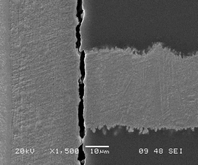
13 Examples of Separation Type ICDs


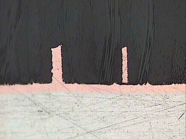
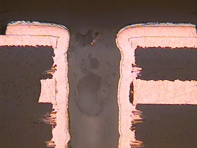
14 Examples of Separation Type ICDs Continued Post Separation Type D-Void Type
15 Getting Rid of ICDs ICD formation is strongly related to two key factors PCB fabricator processes Raw material type Capable and consistent processes in drilling is best approach Avoids creation of ICDs If ICDs are found follow this path Review samples and findings from problem orders Identify the type of ICD Follow troubleshooting method for this type of ICD

16 Debris ICD Type Troubleshooting Drilling Drilling generates the debris that causes most of this type of ICD. Get drill parameters under control Good vacuum levels at drilling Correct chip load Correct cutting speed Bits in good shape, not worn or damaged Beware of combinations of high cutting speed and low chip loads This combination creates high heat levels and more debris Significant copper nailheading is commonly found with Debris based ICDs Reducing nailheading helps reduce debris ICDs Assess drilling quality using SEM of half holes
17 Debris ICD Type Troubleshooting Desmear Desmear removes the debris generated by drilling Good desmear is critical for consistent results If using Plasma Etching, Get weight loss under control Efficient etching Temperature control is the main issue Etch rate rises with time if panels are cool at the start Hot panels may have overetch and plating adhesion issues Dry boards before plasma etching water vapor from dielectric reduces plasma etch effectiveness Measure etch rate on coupon with drilled holes, not surface coupons Weight loss of 30mg/DM2 in holes, or 45-50mg/DM2 for surface coupons is a good target PCB Fab s with good Plasma Etching process have very little ICD issues, when plasma etching is used Best Practices Dry and preheat panels, load panels warm-hot Control weight loss amount and even distribution of weight loss over full load SEM s of half holes is the best tool to characterize Plasma Etching process effectiveness, along with weight loss control.
18 Debris Debugging Chemical Desmear Chemical desmear has two functions Effective at washing out debris Removes resin Removal rate is very dependent on dielectric resin type Chemical desmear issues Sweller type Some materials not compatible with all sweller types particularly NMP type Weight loss Similar to plasma etching, characterize and keep this process under control Chemistry control High MnO2 levels can cause debris to form Agitation, rinsing, ultrasonics Very important on chemical desmear lines Permanganate bathes are very viscous so agitation is critical Good performing PCB fabricators have very good agitation

19 Separation ICDs Strength of Interconnect Creating a strong connection between the innerlayer copper and the electroless copper layer is the best way to avoid ICDs The following is a partial list of factors affecting interconnect strength Good metallurgical copper bond Clean copper, no chemical residues Oxide free copper surface Good grain structure on copper foil Strong electroless copper Appropriate thickness Controlled deposition rate (not to fast) Good grain structure Good hole wall adhesion Copper foil thickness Thicker is better No localized drill damage
20 Separation Type ICD Debugging Strength of bond Determine copper etch weight loss Best over 30u (0.75 um) removed in holes Use good water quality on electroless copper line rinsing Over desmear can also lead to rinsing issues Improve hole wall adhesion Good desmear, with adequate texture Don t over desmear or use too high temperature desmear
21 Separation Type ICD Stress Causes High z-axis expansion High resin content Low TMA Tg High expansion material Poor copper hole wall adhesion Puts strain on interconnects, instead of distributing through out hole wall Design factors Tight grid hole patterns Large hole size Pads only on layers 2 or N-1 Board thickness Localized resin content (regions requiring high resin fill) Solder shrinkage in holes Pulls copper away from hole wall Uncontrolled or over-temperature exposure Poorly controlled solder fountain rework (example) Constraining surface finishes ENIG, Electrolytic Nickel/Gold
22 Separation Type ICD Debugging Stress Reduction Process to achieve good hole wall adhesion Allow options for single ply and heavier glass styles Reduce resin content in the stack-up Do not use nickel plating Avoid design factors As noted on previous slide
23 General Commentary ICDs are rare in the US and Europe Long history of Military and High Reliability electronics has resulted in good processing practices ICDs are PCB process related Strong processes with good process control do not see significant problems Some material types are more likely to have ICDs Materials with inorganic fillers, and more chemically resistant resin systems Require tighter processing windows, or extra desmear steps, to achieve excellent results Plasma etching is more common on these types
24 Summary ICDs are a significant PCB industry issue, primarily in Asia. High performance material systems are more likely to have ICDs Many fabricators have consistently good results, no ICDs Use best practices at drilling and desmear ICD type identification, good engineering, and good controls have been effective at eliminating ICDs Isola and other companies continue to perform Research into the causes of ICDs Working to make the system more robust
FR408 Processing Guide
 FR408 Processing Guide The processing guidelines contained in this document were developed through in-house testing and field experience. However, they should be considered to be starting points that will
Astra MT77 Processing Guide
 Astra MT77 Processing Guide The processing guidelines contained in this document were developed through in-house testing and field experience. However, they should be considered to be starting points that
Low CTE / High Tg FR-4 with High Heat Resistance
 Low CTE / High Tg FR-4 with High Heat Resistance Laminate: EM-827 Prepreg: EM-827B 1 Features Tg(DSC) > 170 Z direction CTE < 3.0% (50~260 ) High thermal degradation temperature: Td > 340 Excellent thermal
PCB Production Process HOW TO PRODUCE A PRINTED CIRCUIT BOARD
 NCAB Group Seminars PCB Production Process HOW TO PRODUCE A PRINTED CIRCUIT BOARD NCAB GROUP PCB Production Process Introduction to Multilayer PCBs 2 Introduction to multilayer PCB s What is a multilayer
Interconnection Reliability of HDI Printed Wiring Boards
 Presented in the ECWC 10 Conference at IPC Printed Circuits Expo, SMEMA Council APEX and Designers Summit 05 Interconnection Reliability of HDI Printed Wiring Boards Tatsuo Suzuki Nec Toppan Circuit Solutions,
Troubleshooting. for. Printed Board. Manufacture. and Assembly IPC PE-740. Revision A December Developed by THE INSTITUTE FOR INTERCONNECTING
 IPC PE-740 Revision A December 1997 Troubleshooting for Printed Board Manufacture and Assembly IPC 1997 Developed by THE INSTITUTE FOR INTERCONNECTING AND PACKAGING ELECTRONIC CIRCUITS December 1997 IPC-PE-740
IS410 Processing Guide
 IS410 Processing Guide The processing guidelines contained in this document were developed through in-house testing and field experience. However, they should be considered to be starting points that will
Flexible PCB Plating Through Hole Considerations, Experiences and Solutions
 Presented in the ECWC 10 Conference at IPC Printed Circuits Expo, SMEMA Council APEX and Designers Summit 05 Flexible PCB Plating Through Hole Considerations, Experiences and Solutions Neil Patton Atotech
IPC-AJ-820A Assembly and Joining Handbook. The How and Why of All Things PCB & PCA
 IPC-AJ-820A Assembly and Joining Handbook The How and Why of All Things PCB & PCA 1 Scope To provide guidelines and supporting info for the mfg of electronic equipment To explain the HOW TO and WHY Discussions
High Frequency Circuit Materials Attributes John Coonrod, Rogers Corporation
 High Frequency Circuit Materials Attributes John Coonrod, Rogers Corporation Specialty high frequency circuit materials have been used in the PCB industry for decades and for many different reasons. There
NCAB Group PCB Specification
 NCAB Group Seminar no. 9 NCAB Group PCB Specification NCAB GROUP NCAB Group PCB Specification 14 key features for durable and reliable PCB s NCAB GROUP NCAB Group PCB Specification 2 Are all PCB s created
Thermal Reliability of Laser Ablated Microvias and Standard Through-Hole Technologies as a Function of Materials and Processing
 Thermal Reliability of Laser Ablated Microvias and Standard Through-Hole Technologies as a Function of Materials and Processing Todd Young Isola Frank Polakovic and Michael Carano Electrochemicals Inc.
Introduction Conductors. Supply Planes. Dielectric. Vias PCB Manufacturing Process Electronic Assembly Manufacturing Process
 PCBs/Overview Printed Circuit Boards (PCB) Introduction Conductors. Supply Planes. Dielectric. Vias PCB Manufacturing Process Electronic Assembly Manufacturing Process 29/09/2005 EE6471 (KR) 263 PCBs/Overview
ATS Document Cover Page
 221-008 Item Rev Status: RELEASED printed 9/20/2017 2:27:42 PM by Les Deenin ATS: OPERATIN PROCEDURE ATS Document Cover Page Responsible Department: Supply Chain This copy is uncontrolled unless otherwise
Via Life vs. Temperature Stress Analysis of Interconnect Stress Test
 Page 1 of 12 N P All BNP Media LINX Search H i 3 w Want to use this article? CLICK HERE for options!
How to select PCB materials for highfrequency
 How to select PCB materials for highfrequency apps Find out how to simplify that choice when striving for the best tradeoff between ease of fabrication and best electrical performance. By John Coonrod
High Tg Bromine-free Laminates for PWB Applications
 Presented at IPC Printed Circuits EXPO www.ipcprintedcircuitexpo.org High Tg Bromine-free Laminates for PWB Applications Marty Choate Isola Abstract The development of halogen free materials has been a
Qualification and Performance Specification for Flexible Printed Boards
 Qualification and Performance Specification for Flexible Printed Boards Developed by the Flexible Circuits Performance Specifications Subcommittee (D-12) of the Flexible Circuits Committee (D-10) of IPC
GRAPHIC MANUFACTURING CAPABILITY Q217-18
 All features are design dependent and may not be achievable in combination Reduced Yield / Special values up ( or down ) to the standard limit are design and application dependent Standard features only
RF-43. General Processing Guidelines
 RF-43 General Processing Guidelines Petersburgh, NY Tel: 800-833-1805 Fax: 518-658-3988 Europe Tel: +353-44-38300 Fax: +353-44-44369 Asia Tel: +82-31-704-1858 Fax: +82-31-704-1857 www.taconic-add.com www.taconic.co.kr
U.S. EPA-IPC Design for the Environment Printed Wiring Board Project Making Holes Conductive Performance Testing Results
 U.S. EPA-IPC Design for the Environment Printed Wiring Board Project Making Holes Conductive Performance Testing Results Introduction Methods and Materials Discussion Acknowledgments Appendices: 1. Test
Freescale Semiconductor Tape Ball Grid Array (TBGA) Overview
 Overview") Freescale Semiconductor Tape Ball Grid Array (TBGA) Overview Revision 0 2006 Freescale and the Freescale logo are trademarks of Freescale Semiconductor, Inc. All other product or service names are the
Freescale Semiconductor Tape Ball Grid Array (TBGA) Overview Revision 0 2006 Freescale and the Freescale logo are trademarks of Freescale Semiconductor, Inc. All other product or service names are the
MCPCB Material (Heat sync)
") MCPCB Material (Heat sync) NIPPON RIKA KOGYOSHO CO.,LTD Feb Metal Base CCL (Heat sync) Metal Base CCL (Heat sync) Copper Foil FR-4 High Performance Epoxy Metal Base Glass Cloth + Epoxy Etching Etching
MCPCB Material (Heat sync) NIPPON RIKA KOGYOSHO CO.,LTD Feb Metal Base CCL (Heat sync) Metal Base CCL (Heat sync) Copper Foil FR-4 High Performance Epoxy Metal Base Glass Cloth + Epoxy Etching Etching
Discrete Capacitor & Resistor Issues. Anthony Primavera Boston Scientific CRM 11/13/06
 Discrete Capacitor & Resistor Issues Anthony Primavera Boston Scientific CRM 11/13/06 Goal: Drive the Industry towards common test methods and best practices in manufacturing to reduce and or eliminate
PEC (Printed Electronic Circuit) process for LED interconnection
 process for LED interconnection") PEC (Printed Electronic Circuit) process for LED interconnection Higher wattage LED s/ power components or their placement in higher densities, requires a larger dissipation of heat in a more effective
PEC (Printed Electronic Circuit) process for LED interconnection Higher wattage LED s/ power components or their placement in higher densities, requires a larger dissipation of heat in a more effective
EFFECT OF THE MICROSTRUCTURE OF Ni/Au METALLIZATION ON BONDABILITY OF FR-4 SUBSTRATE
 EFFECT OF THE MICROSTRUCTURE OF Ni/Au METALLIZATION ON BONDABILITY OF FR-4 SUBSTRATE Zonghe Lai and Johan Liu The Swedish Institute of Production Engineering Research (IVF) S-431 53 Mölndal, Sweden ABSTRACT
SITV s Stack-ups and Loss. Add a subtitle
 SITV s Stack-ups and Loss Add a subtitle SITV Stack-ups General Signal Integrity TV s are often used to characterize material performance There are a variety of TV s that use differing approaches and measurement
2015 IEEE. REPRINTED, WITH PERMISSION, FROM Next Generation Metallization Technique for IC Package Application
 2015 IEEE. REPRINTED, WITH PERMISSION, FROM Next Generation Metallization Technique for IC Package pplication Yoshiyuki Hakiri, Katsuhiro Yoshida, Shenghua Li, Makoto Kondoh, Shinjiro Hayashi The Dow Chemical
Via Filling: Challenges for the Chemistry in the Plating Process
 Via Filling: Challenges for the Chemistry in the Plating Process Mike Palazzola Nina Dambrowsky and Stephen Kenny Atotech Deutschland GmbH, Germany Abstract Copper filling of laser drilled blind micro
IBM Laminate Study Group
 IBM Laminate Study Group Lead-Free Laminate Robustness Brett Krull, Dept FM2 Nov 18, 2009 Agenda Introductions Laminate Robustness Background Qualification Methods Contributing Factors Past Work on Laminate
Cleaning Before Coating. Presented by Jigar Patel, Senior Process Engineer
 Cleaning Before Coating Presented by Jigar Patel, Senior Process Engineer Cleaning Before Coating Influencing factors Failure mechanisms Coating failures Cleaning before coating Analytics and test methods
Process & Capability Manual (Vol )
") Process & Capability Manual (Vol. 12-2015) Seite 1 von 13 1 CHAPTER OVERVIEW 1 CHAPTER OVERVIEW... 2 2 MICROCIRTEC A SHORT PROFILE... 3 2.1 WHO WE ARE... 3 2.2 OBJECTIVES & MARKETS... 3 2.3 DECLARATION
Process & Capability Manual (Vol. 12-2015) Seite 1 von 13 1 CHAPTER OVERVIEW 1 CHAPTER OVERVIEW... 2 2 MICROCIRTEC A SHORT PROFILE... 3 2.1 WHO WE ARE... 3 2.2 OBJECTIVES & MARKETS... 3 2.3 DECLARATION
Ultra Fine Pitch Bumping Using e-ni/au and Sn Lift-Off Processes
 Ultra Fine Pitch Bumping Using e-ni/au and Sn Lift-Off Processes Andrew Strandjord, Thorsten Teutsch, and Jing Li Pac Tech USA Packaging Technologies, Inc. Santa Clara, CA USA 95050 Thomas Oppert, and
WF6317. A superactive low-volatile/high heat-resistant water-soluble flux for ball soldering
 WF637 A superactive low-volatile/high heat-resistant water-soluble flux for ball soldering Low viscosity and high tacking power stabilize ball holding force and ensures excellent solder wettability Easy
Optimizing the Insulated Metal Substrate Application with Proper Material Selection and Circuit Fabrication
 Abstract Optimizing the Insulated Metal Substrate Application with Proper Material Selection and Circuit Fabrication Dave Sommervold, Chris Parker, Steve Taylor, Garry Wexler. The Bergquist Company Prescott,
UL PCB Recognition what is it & why do you need to know about it
 UL PCB Recognition what is it & why do you need to know about it Presented by Emma Hudson NCAB Customer Event March 2015 UL and the UL logo are trademarks of UL LLC 2015 Agenda What is UL and what are
IPC-TM-650 TEST METHODS MANUAL
 3000 Lakeside Drive, Suite 309S Bannockburn, IL 60015-1249 TEST METHODS MNUL Number Conductive nodic Filament (CF) Resistance Test: X-Y xis Originating Task Group Electrochemical Migration Task Group (5-32e)
PCB Technologies for LED Applications Application note
 PCB Technologies for LED Applications Application note Abstract This application note provides a general survey of the various available Printed Circuit Board (PCB) technologies for use in LED applications.
inemi BFR-Free Free PCB Material Evaluation Project Chair : Stephen Tisdale Intel Corporation SMTAi Presentation August 21, 2008
 inemi BFR-Free Free PCB Material Evaluation Project Chair : Stephen Tisdale Intel Corporation SMTAi Presentation August 21, 2008 0 Co-Authors Gary B. Long Intel Corporation Hillsboro, OR Gary.B.Long@Intel.com
HBLED packaging is becoming one of the new, high
 Ag plating in HBLED packaging improves reflectivity and lowers costs JONATHAN HARRIS, President, CMC Laboratories, Inc., Tempe, AZ Various types of Ag plating technology along with the advantages and limitations
ThunderClad 2. TU-883 HF Very Low Loss Material. Laminates & Prepregs Mass Lamination Service Insulated Metal Substrate Materials
 ThunderClad 2 TU-883 HF Very Low Loss Material Laminates & Prepregs Mass Lamination Service Insulated Metal Substrate Materials TUC Product Roadmap 2 ULVP VLP HCF Ultra Low Void Prepreg Very Low Profile
IMPACT OF MICROVIA-IN-PAD DESIGN ON VOID FORMATION
 IMPACT OF MICROVIA-IN-PAD DESIGN ON VOID FORMATION Frank Grano, Felix Bruno Huntsville, AL Dana Korf, Eamon O Keeffe San Jose, CA Cheryl Kelley Salem, NH Joint Paper by Sanmina-SCI Corporation EMS, GTS
Flex and Rigid-Flex Printed Circuit Design
 Flex and Rigid-Flex Printed Circuit Design Old Content - visit altium.com/documentation Modified by on 29-Nov-2016 Related Videos Bending Lines Enhanced Layer Stack Management Layer Stack Regions A rigid-flex
TAIYO THP-100DX1 USA-SP (UL Name: THP-100DX)
") TAIYO THP-100DX1 USA-SP (UL Name: THP-100DX) THP-100DX1 USA-SP after copper plating. THP-100DX1 USA-SP in 1 and 5 kg container. Available in a 1 and 5 kg container One-component Thermally Cured Hole Fill
TAIYO THP-100DX1 USA-SP (UL Name: THP-100DX) THP-100DX1 USA-SP after copper plating. THP-100DX1 USA-SP in 1 and 5 kg container. Available in a 1 and 5 kg container One-component Thermally Cured Hole Fill
PRELIMINARY. FRSH Series (0603, 0805, 1206, 1506, 2010, 2512) (Z1-Foil) Vishay Foil Resistors
 (Z1-Foil) Vishay Foil Resistors") Ultra High Precision Foil Wraparound Surface Mount Chip Resistor with Extended Pads for High Power/High Temperature Applications up to +225 C, Load Life Stability of 0.05%,TCR to ± 1ppm/ C INTRODUCTION
Ultra High Precision Foil Wraparound Surface Mount Chip Resistor with Extended Pads for High Power/High Temperature Applications up to +225 C, Load Life Stability of 0.05%,TCR to ± 1ppm/ C INTRODUCTION
TECHNICAL DATA SHEET 1 P a g e Revised January 9, 2014
 1 P age Revised January 9, 2014 TAIYO PSR-4000 CC01SE (UL Name: PSR-4000JV / CA-40JV) LIQUID PHOTOIMAGEABLE CURTAIN COAT SOLDER MASK Curtain Coat Application Aqueous Developing Solder Mask RoHS Compliant
Selection and Application of Board Level Underfill Materials
 Selection and Application of Board Level Underfill Materials Developed by the Underfill Materials Design, Selection and Process Task Group (5-24f) of the Assembly and Joining Committee (5-20) of IPC Supersedes:
Reliability of Interconnects in LED Lighting Assemblies Utilizing Metal Clad Printed Circuit Boards Stefano Sciolè BDM I.M.S.
 Reliability of Interconnects in LED Lighting Assemblies Utilizing Metal Clad Printed Circuit Boards Stefano Sciolè BDM I.M.S. Henkel Electronic Materials Agenda 1. Introduction 2. Motivation 3. Interconnect
Newsletter. Test Services & Failure Analysis Laboratory. April The Reality of Flip-Chip Solder Bump Electromigration Failure INSIDE THIS ISSUE
 Test Services & Failure Analysis Laboratory April 2008 Newsletter INSIDE THIS ISSUE Features Solder Bump Electromigration Failure Solder Joint Failure Criteria External Inspection of PCBs Hollow Fibers
Jacques Matteau. NanoBond Assembly: A Rapid, Room Temperature Soldering Process. Global Sales Manager. indium.us/f018
 Jacques Matteau Global Sales Manager NanoBond Assembly: A Rapid, Room Temperature Soldering Process jmatteau@indium.com indium.us/f014 indium.us/f018 Terminology A few key terms NanoFoil is the heat source
contaminated, or if the location of the assembly house is well above sea level.
 VAPOR PHASE REFLOW S EFFECT ON SOLDER PASTE RESIDUE SURFACE INSULATION RESISTANCE Karen Tellefsen. Mitch Holtzer, Corne Hoppenbrouwers Alpha Assembly Solutions South Plainfield, NJ, USA Roald Gontrum SmartTech
Component Palladium Lead Finish - Specification Approved by Executive Board 1997-xx-xx August 22 Version
 Component Palladium Lead Finish - Specification Approved by Executive Board 1997-xx-xx August 22 Version Appendices 1. User Commitment Form 2. Supplier Compliance Form Table of contents 1. Background 2.
3M Electromagnetic Compatible Products
 3M Electromagnetic Compatible Products Selection Guide Revision E 3 Innovation Faster, smaller, lighter, easier the skyrocketing development of today s electronics requires new solutions for significant
Metallization deposition and etching. Material mainly taken from Campbell, UCCS
 Metallization deposition and etching Material mainly taken from Campbell, UCCS Application Metallization is back-end processing Metals used are aluminum and copper Mainly involves deposition and etching,
Innovative MID Plating Solutions
 Innovative MID Plating Solutions High Reliability Wire Bond Technique for MIDs Jordan Kologe MacDermid Electronics Solutions jkologe@macdermid.com 1 MacDermid: Specialty Chemical Solutions Over 2000 Worldwide
Ultralow Residue Semiconductor Grade Fluxes for Copper Pillar Flip-Chip
 Ultralow Residue Semiconductor Grade Fluxes for Copper Pillar Flip-Chip SzePei Lim (Presenter), Jason Chou, Maria Durham, and Dr. Andy Mackie Indium Corporation 1 Outline of Presentation Roadmaps and challenges
Lead-Free Solder Bump Technologies for Flip-Chip Packaging Applications
 Lead-Free Solder Bump Technologies for Flip-Chip Packaging Applications Zaheed S. Karim 1 and Jim Martin 2 1 Advanced Interconnect Technology Ltd. 1901 Sunley Centre, 9 Wing Yin Street, Tsuen Wan, Hong
3 Thermally Conductive Tapes
 3 Thermally Conductive Tapes Technical Data July, 21 Product Description 3M Thermally Conductive Tapes 885, 881, and 8815 are designed to provide a preferential heat-transfer path between heat-generating
Recent Advances in Die Attach Film
 Recent Advances in Die Attach Film Frederick Lo, Maurice Leblon, Richard Amigh, and Kevin Chung. AI Technology, Inc. 70 Washington Road, Princeton Junction, NJ 08550 www.aitechnology.com Abstract: The
c/bach, 2-B Pol. Ind Foinvasa Montcada i Reixac (Barcelona) SPAIN Tel FAX
 SPAIN Tel FAX") 1- What is 2- How does it work? 3- How do we make it? 4- Applications 5- Processing? WHAT IS? Thick aluminium based substrate, cladded in ED copper foil. Designed for an effective thermal dissipation and
1- What is 2- How does it work? 3- How do we make it? 4- Applications 5- Processing? WHAT IS? Thick aluminium based substrate, cladded in ED copper foil. Designed for an effective thermal dissipation and
COFAN USA. Meeting your Project needs.
 COFAN USA Meeting your Project needs www.cofangroup.com PCB Substrate Pre-preg Category SEKISUI Laird T-Clad Denka PCB Substrate Pre-preg Category In the PCB industry, there are a couple major Pre-preg
System Level Effects on Solder Joint Reliability
 System Level Effects on Solder Joint Reliability Maxim Serebreni 2004 2010 Outline Thermo-mechanical Fatigue of solder interconnects Shear and tensile effects on Solder Fatigue Effect of Glass Style on
Flexible Printed Circuits Design Guide
 www.tech-etch.com/flex Flexible Printed Circuits Design Guide Multilayer SMT Assembly Selective Plating of Gold & Tin-Lead Fine Line Microvias Cantilevered & Windowed Leads 1 MATERIALS CONDUCTOR Copper
Lead Free Surface Mount Technology. Ian Wilding BSc Senior Applications Engineer Henkel Technologies
 Lead Free Surface Mount Technology Ian Wilding BSc Senior Applications Engineer Henkel Technologies Overview of the Presentation First contact: Impact on the production operator Packaging Labelling Impact
Characterizing the Lead-Free Impact on PCB Pad Craters
 Characterizing the Lead-Free Impact on PCB Pad Craters Brian Roggeman and Wayne Jones Advanced Process Lab Universal Instruments Corp. Binghamton, NY 13902 Abstract Pad cratering in Printed Circuit Boards
Thermo-Mechanical Reliability of Through-Silicon Vias (TSVs)
") 1 Thermo-Mechanical Reliability of Through-Silicon Vias (TSVs) Xi Liu Ph.D. Student and Suresh K. Sitaraman, Ph.D. Professor The George W. Woodruff School of Mechanical Engineering Georgia Institute of
1 Thermo-Mechanical Reliability of Through-Silicon Vias (TSVs) Xi Liu Ph.D. Student and Suresh K. Sitaraman, Ph.D. Professor The George W. Woodruff School of Mechanical Engineering Georgia Institute of
Highly Accelerated Thermal Shock Reliability Testing
 Highly Accelerated Thermal Shock Reliability Testing by Bob E. Neves Microtek Laboratories, Inc. Anaheim CA and Rick B. Snyder Delphi Delco Electronics Systems, Inc. Kokomo IN and Timothy A. Estes Conductor
White Paper Quality and Reliability Challenges for Package on Package. By Craig Hillman and Randy Kong
 White Paper Quality and Reliability Challenges for Package on Package By Craig Hillman and Randy Kong Background Semiconductor technology advances have been fulfilling Moore s law for many decades. However,
INTERFLUX ELECTRONICS NV
 Reflow soldering temperature profiling Min : 30sec Max : 120sec Max : +4 C/sec Max : 250 C Min : 230 C Min: +0,5 C/sec Min : +1 C/sec Max : +3 C/sec Max : +1 C/sec Max : -6 C/sec Min : -2 C/sec Min : +1
Tooling gelcoat MGS F 300
 3-15 Tooling gelcoat MGS Hardener MGS page Characteristics 15 Application 16 Specifications 20 Processing details 20 Mixing ratios 20 DMA 21 Content Application tooling Characteristics Operational temperature
Insulated Metal Substrates
 Insulated Metal Substrates Presented by Les Round of Spirit Circuits ICT Evening Seminar: 15 th September 2010 Venue: Newtown Hotel, Hayling Island Why use Thermal Management The failure rate of an electronic
Basic PCB Level Assembly Process Methodology for 3D Package-on-Package
 Basic PCB Level Assembly Process Methodology for 3D Package-on-Package Vern Solberg STC-Madison Madison, Wisconsin USA Abstract The motivation for developing higher density IC packaging continues to be
The hand soldering process can therefore be defined by the following steps ;
 Hand Soldering with Lead Free Alloys Introduction As companies start to implement lead free soldering processes, hand soldering and associated techniques have been identified as key functions in the manufacturing
Chips Face-up Panelization Approach For Fan-out Packaging
 Chips Face-up Panelization Approach For Fan-out Packaging Oct. 15, 2015 B. Rogers, D. Sanchez, C. Bishop, C. Sandstrom, C. Scanlan, TOlson T. REV A Background on FOWLP Fan-Out Wafer Level Packaging o Chips
23 rd ASEMEP National Technical Symposium
 THE EFFECT OF GLUE BOND LINE THICKNESS (BLT) AND FILLET HEIGHT ON INTERFACE DELAMINATION Raymund Y. Agustin Janet M. Jucar Jefferson S. Talledo Corporate Packaging & Automation/ Q&R STMicroelectronics,
Precision Engineered Parts
 Precision Engineered Parts Photoetching Laser Cutting Forming Finishing Thin Metal Parts Flexible Circuits EMI Shielding Gaskets www.tech-etch.com PHOTOETCHING Tech-Etch specializes in the manufacture
OPTIMIZED SEMI-ADDITIVE PROCESS FOR POLYIMIDE AS DIELECTRIC IN BUILD UP PACKAGES
 OPTIMIZED SEMI-ADDITIVE PROCESS FOR POLYIMIDE AS DIELECTRIC IN BUILD UP PACKAGES Fei Peng 1, Ernest Long 1, Jim Watkowski 1, Kesheng Feng 1, Naomi Ando 2, Kazuhiro Inazu 2 1 MacDermid, 227 Freight St,
Reference Only. Spec. No. JENF243D-0006K-01 P 1/ 8
 Spec. No. JENF243D-0006K-01 P 1/ 8 Chip EMIFIL LC Combined Monolithic NFL21SP X1C Reference Specification 1. Scope This reference specification applies to Chip EMIFIL LC Combined Monolithic Type NFL21S
Nano- And Micro-Filled Conducting Adhesives For Z-axis Interconnects
 Nano- And Micro-Filled Conducting Adhesives For Z-axis Interconnects We take a look at micro-filled epoxy-based conducting adhesives modified with nanoparticles for z- axis interconnections, especially
PRELIMINARY. HTHA (Z1-Foil)
") Ultra High Precision Z1-Foil Technology Chip Resistor for Hybrid Circuits with Aluminum Wire Bonding for High Temperature Applications up to +240 C, Long Term Stability of 0.05%, TCR to ± 1ppm/ C INTRODUCTION
Ultra High Precision Z1-Foil Technology Chip Resistor for Hybrid Circuits with Aluminum Wire Bonding for High Temperature Applications up to +240 C, Long Term Stability of 0.05%, TCR to ± 1ppm/ C INTRODUCTION
HTHA (Z1-Foil) Vishay Foil Resistors
 Vishay Foil Resistors") Ultra High Precision Z1-Foil Technology Chip Resistor for Hybrid Circuits with Aluminum Wire Bonding for High Temperature Applications up to +240 C, Long Term Stability of 0.05%, TCR to ± 1ppm/ C INTRODUCTION
Ultra High Precision Z1-Foil Technology Chip Resistor for Hybrid Circuits with Aluminum Wire Bonding for High Temperature Applications up to +240 C, Long Term Stability of 0.05%, TCR to ± 1ppm/ C INTRODUCTION
Ceramic Column Grid Array Design and Manufacturing Rules for Flight Hardware
 GODDARD TECHNICAL STANDARD GSFC-STD-6001 Goddard Space Flight Center Approved: 02-22-2011 Greenbelt, MD 20771 Expiration Date: 02-22-2016 Superseding GSFC-STD-XXXXR Ceramic Column Grid Array Design and
Lead Free Assembly: A Practical Tool For Laminate Materials Selection
 Lead Free Assembly: A Practical Tool For Laminate Materials Selection Erik J. Bergum David Humby Isola Abstract: The impending European RoHS legislation, restricting the use of lead containing solders,
LOW TEMPERATURE PHOTONIC SINTERING FOR PRINTED ELECTRONICS. Dr. Saad Ahmed XENON Corporation November 19, 2015
 LOW TEMPERATURE PHOTONIC SINTERING FOR PRINTED ELECTRONICS Dr. Saad Ahmed XENON Corporation November 19, 2015 Topics Introduction to Pulsed Light Photonic sintering for Printed Electronics R&D Tools for
Design and Assembly Process Implementation of 3D Components
 IPC-7091 Design and Assembly Process Implementation of 3D Components Developed by the 3-D Electronic Packages Subcommittee (B-11) of the Packaged Electronic Components Committee (B-10) of IPC Users of
SCV Chapter, CPMT Society, IEEE September 14, Voids at Cu / Solder Interface and Their Effects on Solder Joint Reliability
 Voids at / Solder Interface and Their Effects on Solder Joint Reliability Zequn Mei, Mudasir Ahmad, Mason Hu, Gnyaneshwar Ramakrishna Manufacturing Technology Group Cisco Systems, Inc. Acknowledgement:
Offshore Wind Turbines Power Electronics Design and Reliability Research
 Offshore Wind Turbines Power Electronics Design and Reliability Research F. P. McCluskey CALCE/Dept. Of Mechanical Engineering University of Maryland, College Park, MD (301) 405-0279 mcclupa@umd.edu 1
Keeping Cool!: selecting high performance thermal materials for LED Lighting applications. Ian Loader 25/03/14
 Keeping Cool!: selecting high performance thermal materials for LED Lighting applications Ian Loader 25/03/14 1 Target Points to cover Basics of Thermal Management Considerations for thermal materials
THIN IMMERSION TIN USING ORGANIC METALS
 THIN IMMERSION TIN USING ORGANIC METALS Jim Kenny, Nils Arendt, Bernhard Wessling, and Karl Wengenroth Enthone Inc., A Business of Cookson Electronics West Haven, CT, USA ABSTRACT With the international
EIPC Summer Conference Luxembourg Paper 4
 EIPC Summer Conference Luxembourg 2013 PCB differentiation through technology - made in Europe Paper 4 Copper plating process for filling micro vias and through via holes with minimum surface deposition
Intel Pentium Processor W/MMX
 Construction Analysis Intel Pentium Processor W/MMX Report Number: SCA 9706-540 Global Semiconductor Industry the Serving Since 1964 15022 N. 75th Street Scottsdale, AZ 85260-2476 Phone: 602-998-9780 Fax:
ESPANEX L Series. Technical data sheet Nishigotanda Shinagawa Tokyo, , Japan TEL FAX
 ESPANEX L Series Technical data sheet This sheet will be changed without any information in advance. The data on this sheet are solely for your reference and are not to be constructed as constituting a
Conductive Anodic Filament Growth Failure
 Presented at IPC Printed Circuits Expo www.ipcprintedcircuitexpo.org Conductive Anodic Filament Growth Failure Tarun Amla Isola Abstract With increasing focus on reliability and miniaturized designs, Conductive
Your partner solutions
 The Flatstar series is a modular grinding machine for removing the residues of resins, pastes and inks after the hole plugging process in the production of printed circuit boards Your partner solutions
THE SEVEN SINS OF LEAD FREE SOLDERING TRAINING CERTIFICATION TEST (DVD-70C) v.2
 v.2") This test consists of twenty multiple-choice questions. All questions are from the video: The Seven Sins of Lead Free Soldering (DVD-70C). Each question has only one most correct answer. Circle the letter
This test consists of twenty multiple-choice questions. All questions are from the video: The Seven Sins of Lead Free Soldering (DVD-70C). Each question has only one most correct answer. Circle the letter