Donald Neamen 물리전자 / 김삼동 1-1
|
|
|
- Mervyn Brown
- 6 years ago
- Views:
Transcription
1 An Introduction to Semiconductor Devices Donald Neamen Images and illustrations from supplements of An Introduction to Semiconductor Devices, 4 th Ed., Mc Graw Hill were used for this lecture materials. 1-1
2 Semiconductor Materials Elemental SC - Group 4 elements : C, Si, Ge -Sn, Pb? Compound SC - Intermetallic compound - IV-IV(Si-Ge, Si-C) - III-V(Al-P,As,Sb; Ga-N,P,As,Sb; In-N,P,As,Sb), BN - II-VI(Zn-S,Se,Te; Cd-S,Se,Te; Hg-Se,Te), MgO Alloys - Binary : Si-Ge - Ternary : (Al,Ga)As, (Al,In)As, (Cd,Mn)Te,Ga(As,P), (Ga,In)As, (Ga,In)P, (Hg,Cd)Te - Quaternary : (Al,Ga)(As,Sb), (Ga,In)(As,P) I II III IV V VI VII VIII H He Li Be B C N O F Ne Na Mg Al Si P S Cl Ar K Ca/Zn Ga Ge As Se Br Kr Cd In Sn Sb Te Hg Ti Pb Bi 1-2
3 Semiconductor History 1833; Fist semiconducting property of Ag 2 S by Faraday 1873; Discovery of photoconductivity of Se by Smith 1874; Observation of rectification by Braun 1879; Discovery of Hall effect (electron not yet discovered) d) 1911; The term semiconductor introduced by Konigsberg & Weiss 1927; copper oxide rectifier by Grondahl & Geiger 1931; photocell by Bergmann 1939; Development of microwave (Si) 1940s; IR detectors of sulphide, selenide, telluride 1949; Discovery of transistor action by Bardeen & Brattain 1950; Invention of transistor by Shockley, First amorphous semiconductor (α-se) ~ present; IC (electronic industry), solid state laser, organic semiconductors, artificial compound semiconductors 1-3
4 Physical Constants and units Avogadro's number: N A Boltzmann's constant k joule K Electronic charge (magnitude): e ( coul ) Free electron rest mass m e ( kg ) Permeability of free space: μ 0 ( 4. π ) m Permittivity of free space ε farad cm Planck's constant: h ( joule. sec ) Proton rest mass m p ( kg ) Speed of light in vacuum: c cm sec ev joule (electron-volt) mev ev μsec sec na amp pa amp V volt μm m nm m Angstrom m Å m 1-4
5 Amorphous materials (for instance, glass and rubber) have order within a few atomic or molecular dimensions. Polycrystalline materials have a high degree of order over many atomic or molecular dimensions. These ordered regions, or single-crystal regions, vary in size and orientation with respect to one another. The single-crystal regions are called grains and are separated from one another by grain boundaries. Single-crystal materials ( for example, silicon, copper, and table salt) have a very high degree of order, or regular geometric periodicity, throughout their entire volume. The advantage of a single-crystal material is that, in general, its electrical properties are superior to those of a nonsingle-crystal material, since grain boundaries tend to degrade the electrical characteristics. Types of Solids 1-5


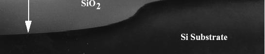
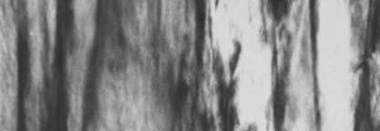
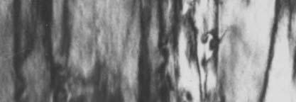
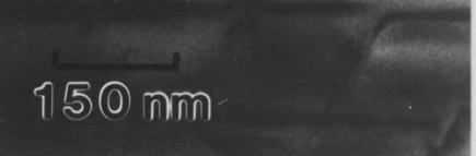
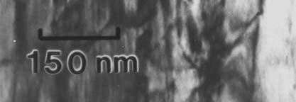
6 SiO 2 2/Si HRXTEM view of Si/SiO 2 1-6
7 Defects in Material Point defect (0-D) Surface defect (2-D) Vacancy Grain boundary Interstitial ex) Impurities Substitutional impurity Bulk defect (3-D) Interstitial impurity Precipitate Line defect (1-D) Edge dislocationline 1-7
8 Point Defects A vacancy in the crystal. A substitutional impurity in the crystal. The impurity atom is larger than the host atom. A substitutional impurity in the crystal. The impurity atom is smaller than the host atom. An interstitial impurity in the crystal. It occupies an empty space between host atoms. 1-8
9 Line Defects Compression Tension A Dislocation line D C Ascrew dislocation in a crystal. A edge dislocation in a crystal is a line defect which is accompanied by lattice distortion and hence a lattice strain around it. Dislocation A B line Atoms in the lower portion. Atoms in the upper portion. D C The screw dislocation in as viewed from above. 1-9


10 Line Defects InGaAs/AlGaAs QWs dislocations 1-10
11 Surface Defects Nuclei Crystallite Liquid (a) (b) Grain Grain boundary Foreign impurity Self-interstitial type atom Void, vacancy Strained bond Grain boundary Broken bond (dangling bond) (c) Solidification of a polycrystalline solid from the melt. (a) Nucleation. (b) Growth. (c) The solidified polycrystalline solid. For simplicity, cubes represent atoms. 1-11
12 Primitive and Unit cells Lattice Unit cell : Periodic arrangement of atoms in the crystal Dots can be used for representing the atomic arrays : Lattice Primitive unit cell 3-D unit cell Two dimensional lattice - Unit cell : A small of the crystal that can be used to reproduce the entire crystal r = p a + q b + s c (p, q, s = integers) 1-12
13 Basic Crystal Structures Cubic Lattices Simple Cubic (SC) Body-Centered Cubic (BCC) Face-Centered Cubic (FCC) (000) (000) (000) Q1: How many atoms are included in each unit cell? Q2: What are the packing densities? 1-13
14 Miller index Lattice direction c z UnitCell Geometry z Unit cell c β O α b y γ a a b x A parallelepiped is chosen to describe geometry of a unit cell. We line the x, y and z axes with the edges of the parallelepiped taking lower-left rear corner as the origin [001] x c x o z o P [121] b a y o Identification of a direction in a crystal [111] y [010] [010] -y -a a [100] [110] x [110] [111] [111] [111] [111] Directions in cubic crystal system y [111] [111] [111] [111] Family of <111> directions 1-14
15 Crystal plane and Miller index Index of Plane Plane =,, p q s 1-15
16 Crystal plane and Miller index z (010) (010) z (010) (010) z intercept at x intercept at a / 2 x b c Miller Indices (hk ): (210) 1 2 y a Unit cell y intercept at b (100) x (010) y y x (001) (110) z Identification of a plane in a crystal z (110) (111) (111) - y y x y x Various planes in cubic lattices -z 1-16


17 The Structure of Solids and Surfaces Bulk termination : FCC FCC (110) FCC (100) FCC (111) 1-17


18 The Structure of Solids and Surfaces Bulk termination : BCC BCC (110) BCC (100) BCC (111) 1-18
 plane in fcc 8 ( a )( ) ( ) 2 0 2a0 2 4.5 10 Q2: a o = 4.75 Å.")
19 Crystal plane and Miller index ex) Calculate the surface density of (110) plane in fcc. a o = 4.5 Å. 2 atoms 2 atoms Surface density = = Q1: Surface density of (111) plane in fcc 8 ( a )( ) ( ) 2 0 2a Q2: a o = 4.75 Å. Calculate the surface densities = atoms/cm 14 2 of (100) and (110) planes in bcc. 1-19


20 Semiconductor Structure Diamond Cubic Structure 1 [ ] fcc fcc Q1: How many atoms in unit cell? Q2: Coordinates of atoms in unit cell? Q3: What are the packing densities? 1-20
21 Semiconductor Structure Diamond cubic structure has - 8 atoms/unit cell - atomic packing factor = ~34 % - covalent bonding, tetragonal unit, 4 nearest neighbors a 0 0 1/2 0 a 0 /2 3/4 1/2 0 1/4 0 1/2 1/4 3/4 1/2 0 1 [ ] fcc fcc 1-21
22 Semiconductor Structure Zincblende structure - GaAs crystal structure Differs from the diamond structure only in that there are two types of atoms in the lattice 1 4 fcc 4 Ga atoms [ 111] ] fcc 4 4 As atoms, or vice vera. 1-22

23 Semiconductor Growth Purity & Doping - Purity : unintentionally doped (undesired) impurities Si : 1 per 10 9 Si atoms - Dopants : intentionally added impurities Practical functioning of devices Crystal Growth - Electronic grade poly-si Silica Impure silicon SiCl4 Ultrapure SiCl4 Poly-Si Reduction Chlorination Distilation H-Reduction - Single crystal growing Czochralski method Single crystal seed Crystal pulling and rotation 1-23
24 Semiconductor Growth (Mitsubishi website at
25 Semiconductor Growth 1-25
26 Homework Ch.1 4 (d), 7, 10, 14, 16, 19, 25 Due date: 1-26
From sand to silicon wafer
 From sand to silicon wafer 25% of Earth surface is silicon Metallurgical grade silicon (MGS) Electronic grade silicon (EGS) Polycrystalline silicon (polysilicon) Single crystal Czochralski drawing Single
Lecture 2 Silicon Properties and Growth
 Lecture 2 Silicon Properties and Growth Chapters 1 & 2 Wolf and Tauber 1/63 Lecture 2 Why Silicon? Crystal Structure. Defects. Sand to Electronic Grade Polysilicon. Polycrystalline to Single Crystal Silicon.
How to Make Micro/Nano Devices?
 How to Make Micro/Nano Devices? Science: Physics, Chemistry, Biology, nano/biotech Materials: inorganic, organic, biological, rigid/flexible Fabrication: photo/e-beam lithography, self-assembly, D/3D print
PHYSICAL ELECTRONICS(ECE3540) Brook Abegaz, Tennessee Technological University, Fall 2013
 Brook Abegaz, Tennessee Technological University, Fall 2013") PHYSICAL ELECTRONICS(ECE3540) Brook Abegaz, Tennessee Technological University, Fall 2013 1 Chapter 1 The Crystal Structure of Solids Physical Electronics: Includes aspects of the physics of electron movement
PHYSICAL ELECTRONICS(ECE3540) Brook Abegaz, Tennessee Technological University, Fall 2013 1 Chapter 1 The Crystal Structure of Solids Physical Electronics: Includes aspects of the physics of electron movement
Ex: NaCl. Ironically Bonded Solid
 Ex: NaCl. Ironically Bonded Solid Lecture 2 THE STRUCTURE OF CRYSTALLINE SOLIDS 3.2 FUNDAMENTAL CONCEPTS SOLIDS AMORPHOUS CRYSTALLINE Atoms in an amorphous Atoms in a crystalline solid solid are arranged
Order in materials. Making Solid Stuff. Primary Bonds Summary. How do they arrange themselves? Results from atomic bonding. What are they?
 Making Solid Stuff Primary Bonds Summary What are they? Results from atomic bonding So the atoms bond together! Order in materials No long range order to atoms Gases little or no interaction between components
Semiconductors. The essential materials for microelectronics technology A key property: conductivity (or resistivity) - large dynamic range
 - large dynamic range") Semiconductors The essential materials for microelectronics technology A key property: conductivity (or resistivity) - large dynamic range - controllable (or engineerable) Example of controllable conductivity
Semiconductors The essential materials for microelectronics technology A key property: conductivity (or resistivity) - large dynamic range - controllable (or engineerable) Example of controllable conductivity
Agenda o Semiconductor Materials o Crystal Growth o Intrinsic Semiconductors o Extrinsic Semiconductors
 E84 Lecture 3/6/14 K. Candler Agenda o Semiconductor Materials o Crystal Growth o Intrinsic Semiconductors o Extrinsic Semiconductors Introduction A semiconductor is a material that has electrical conductivity
Chapter 1. Crystal Structure
 Chapter 1. Crystal Structure Crystalline solids: The atoms, molecules or ions pack together in an ordered arrangement Amorphous solids: No ordered structure to the particles of the solid. No well defined
ECE440 Nanoelectronics. Lecture 08 Review of Solid State Physics
 ECE440 Nanoelectronics Lecture 08 Review of Solid State Physics A Brief review of Solid State Physics Crystal lattice, reciprocal lattice, symmetry Crystal directions and planes Energy bands, bandgap Direct
Packing of atoms in solids
 MME131: Lecture 6 Packing of atoms in solids A. K. M. B. Rashid Professor, Department of MME BUET, Dhaka Today s topics Atomic arrangements in solids Points, directions and planes in unit cell References:
CRYSTAL STRUCTURE TERMS
 CRYSTAL STRUCTURE TERMS crystalline material - a material in which atoms, ions, or molecules are situated in a periodic 3-dimensional array over large atomic distances (all metals, many ceramic materials,
بسم هللا الرحمن الرحیم. Materials Science. Chapter 3 Structures of Metals & Ceramics
 بسم هللا الرحمن الرحیم Materials Science Chapter 3 Structures of Metals & Ceramics 1 ISSUES TO ADDRESS... How do atoms assemble into solid structures? How does the density of a material depend on its structure?
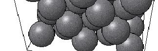
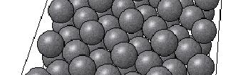
Energy and Packing. typical neighbor bond energy. typical neighbor bond energy. Dense, regular-packed structures tend to have lower energy.
 Energy and Packing Non dense, random packing Energy typical neighbor bond length typical neighbor bond energy r Dense, regular packing Energy typical neighbor bond length typical neighbor bond energy r
Chapter Outline How do atoms arrange themselves to form solids?
 Chapter Outline How do atoms arrange themselves to form solids? Fundamental concepts and language Unit cells Crystal structures Face-centered cubic Body-centered cubic Hexagonal close-packed Close packed
Two marks questions and answers. 1. what is a Crystal? (or) What are crystalline materials? Give examples
 What are crystalline materials? Give examples") UNIT V CRYSTAL PHYSICS PART-A Two marks questions and answers 1. what is a Crystal? (or) What are crystalline materials? Give examples Crystalline solids (or) Crystals are those in which the constituent
UNIT V CRYSTAL PHYSICS PART-A Two marks questions and answers 1. what is a Crystal? (or) What are crystalline materials? Give examples Crystalline solids (or) Crystals are those in which the constituent
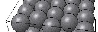
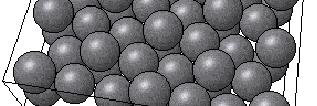
Stacking Oranges. Packing atoms together Long Range Order. What controls the nearest number of atoms? Hard Sphere Model. Hard Sphere Model.
 { Stacking atoms together Crystal Structure Stacking Oranges Packing atoms together Long Range Order Crystalline materials... atoms pack in periodic, 3D arrays typical of: -metals -many ceramics -some
Diffusion & Crystal Structure
 Lecture 5 Diffusion & Crystal Structure Diffusion of an interstitial impurity atom in a crystal from one void to a neighboring void. The impurity atom at position A must posses an energy E to push the
Dept.of BME Materials Science Dr.Jenan S.Kashan 1st semester 2nd level. Imperfections in Solids
 Why are defects important? Imperfections in Solids Defects have a profound impact on the various properties of materials: Production of advanced semiconductor devices require not only a rather perfect
Halbleiter Prof. Yong Lei Prof. Thomas Hannappel
 Halbleiter Prof. Yong Lei Prof. Thomas Hannappel yong.lei@tu-ilmenau.de thomas.hannappel@tu-ilmenau.de http://www.tu-ilmenau.de/nanostruk/ Solid State Structure of Semiconductor Semiconductor manufacturing
Chapter 10. Liquids and Solids
 Chapter 10. Liquids and Solids Three States of Matter H 2 O Volume constant constant no Shape constant no no Why in three different states? 1 Intermolecular Force dipole-dipole attraction V dip-dip : 1.
Engineering 45: Properties of Materials Final Exam May 9, 2012 Name: Student ID number:
 Engineering 45: Properties of Materials Final Exam May 9, 2012 Name: Student ID number: Instructions: Answer all questions and show your work. You will not receive partial credit unless you show your work.
Chapter Outline. How do atoms arrange themselves to form solids?
 Chapter Outline How do atoms arrange themselves to form solids? Fundamental concepts and language Unit cells Crystal structures! Face-centered cubic! Body-centered cubic! Hexagonal close-packed Close packed
Energy and Packing. Materials and Packing
 Energy and Packing Non dense, random packing Energy typical neighbor bond length typical neighbor bond energy r Dense, regular packing Energy typical neighbor bond length typical neighbor bond energy r
Solid State Device Fundamentals
 Solid State Device Fundamentals ENS 345 Lecture Course by Alexander M. Zaitsev alexander.zaitsev@csi.cuny.edu Tel: 718 982 2812 Office 4N101b 1 Solids Three types of solids classified according to atomic
Free Electron Model What kind of interactions hold metal atoms together? How does this explain high electrical and thermal conductivity?
 Electrical Good conductors of heat & electricity Create semiconductors Oxides are basic ionic solids Aqueous cations (positive charge, Lewis acids) Reactivity increases downwards in family Mechanical Lustrous
EE 5611 Introduction to Microelectronic Technologies Fall Tuesday, September 02, 2014 Lecture 01
 EE 5611 Introduction to Microelectronic Technologies Fall 2014 Tuesday, September 02, 2014 Lecture 01 1 Instructor: Jing Bai Contact Email: jingbai@d.umn.edu, hone: (218)726-8606, Office: MWAH 255 Webpage:
VLSI Technology Dr. Nandita Dasgupta Department of Electrical Engineering Indian Institute of Technology, Madras
 VLSI Technology Dr. Nandita Dasgupta Department of Electrical Engineering Indian Institute of Technology, Madras Lecture - 5 Crystal Structure contd So far, we have discussed about the crystal structure
Imperfections, Defects and Diffusion
 Imperfections, Defects and Diffusion Lattice Defects Week5 Material Sciences and Engineering MatE271 1 Goals for the Unit I. Recognize various imperfections in crystals (Chapter 4) - Point imperfections
Chapter 3: Atomic and Ionic Arrangements. Chapter 3: Atomic and Ionic Arrangements Cengage Learning Engineering. All Rights Reserved.
 Chapter 3: Atomic and Ionic Arrangements 3-1 Learning Objectives 1. 2. 3. 4. 5. 6. 7. 8. Short-range order versus long-range order Amorphous materials Lattice, basis, unit cells, and crystal structures
Materials Science ME 274. Dr Yehia M. Youssef. Materials Science. Copyright YM Youssef, 4-Oct-10
 ME 274 Dr Yehia M. Youssef 1 The Structure of Crystalline Solids Solid materials may be classified according to the regularity with which atoms or ions are arranged with respect to one another. A crystalline
METALLIC CRYSTALS. tend to be densely packed. have several reasons for dense packing: have the simplest crystal structures.
 METALLIC CRYSTALS tend to be densely packed. have several reasons for dense packing: -Typically, only one element is present, so all atomic radii are the same. -Metallic bonding is not directional. -Nearest
General Objective. To develop the knowledge of crystal structure and their properties.
 CRYSTAL PHYSICS 1 General Objective To develop the knowledge of crystal structure and their properties. 2 Specific Objectives 1. Differentiate crystalline and amorphous solids. 2. To explain nine fundamental
Free Electron Model What kind of interactions hold metal atoms together? How does this explain high electrical and thermal conductivity?
 Electrical Good conductors of heat & electricity Create semiconductors Oxides are basic ionic solids Aqueous cations (positive charge, Lewis acids) Reactivity increases downwards in family Free Electron
EE 5611 Introduction to Microelectronic Technologies Fall Tuesday, September 04, 2012 Lecture 01
 EE 5611 Introduction to Microelectronic Technologies Fall 2012 Tuesday, September 04, 2012 Lecture 01 1 Instructor: Jing Bai Contact Email: jingbai@d.umn.edu, hone: (218)726-8606, Office: MWAH 255 Webpage:
Chapter 2 Crystal Growth and Wafer Preparation
 Chapter 2 Crystal Growth and Wafer Preparation Professor Paul K. Chu Advantages of Si over Ge Si has a larger bandgap (1.1 ev for Si versus 0.66 ev for Ge) Si devices can operate at a higher temperature
 Solid State-1 1) Ionic solids are characterised by 1) Good conductivity in solid state 2) High vapour pressure 3) Low melting point 4) Solubility in polar solvents 2) Three metals X, Y and Z are crystallised
CHAPTER 5 IMPERFECTIONS IN SOLIDS PROBLEM SOLUTIONS
 CHAPTER 5 IMPERFECTIONS IN SOLIDS PROBLEM SOLUTIONS Vacancies and Self-Interstitials 5.1 Calculate the fraction of atom sites that are vacant for copper at its melting temperature of 1084 C (1357 K). Assume
Solids. The difference between crystalline and non-crystalline materials is in the extent of ordering
 Chapter 3 The Structure t of Crystalline Solids The difference between crystalline and non-crystalline materials is in the extent of ordering Both materials have the same composition but one is ordered
Materials Science and Engineering
 Introduction to Materials Science and Engineering Chap. 3. The Structures of Crystalline Solids How do atoms assemble into solid structures? How does the density of a material depend on its structure?
ENGINEERING MATERIALS LECTURE #4
 ENGINEERING MATERIALS LECTURE #4 Chapter 3: The Structure of Crystalline Solids Topics to Cover What is the difference in atomic arrangement between crystalline and noncrystalline solids? What features
CHAPTER 5 IMPERFECTIONS IN SOLIDS PROBLEM SOLUTIONS ev /atom = exp. kt ( =
 CHAPTER 5 IMPERFECTIONS IN SOLIDS PROBLEM SOLUTIONS Vacancies and Self-Interstitials 5.1 Calculate the fraction of atom sites that are vacant for copper at its melting temperature of 1084 C (1357 K). Assume
IMPERFECTIONSFOR BENEFIT. Sub-topics. Point defects Linear defects dislocations Plastic deformation through dislocations motion Surface
 IMPERFECTIONSFOR BENEFIT Sub-topics 1 Point defects Linear defects dislocations Plastic deformation through dislocations motion Surface IDEAL STRENGTH Ideally, the strength of a material is the force necessary
CHAPTER 3: CRYSTAL STRUCTURES & PROPERTIES
 CHAPTER 3: CRYSTAL STRUCTURES & PROPERTIES ISSUES TO ADDRESS... How do atoms assemble into solid structures? (for now, focus on metals) How does the density of a material depend on its structure? When
Solid State Device Fundamentals
 Solid State Device Fundamentals ENS 345 Lecture Course by Alexander M. Zaitsev alexander.zaitsev@csi.cuny.edu Tel: 718 982 2812 Office 4N101b 1 Interatomic bonding Bonding Forces and Energies Equilibrium
much research (in physics, chemistry, material science, etc.) have been done to understand the difference in materials properties.
 have been done to understand the difference in materials properties.") 1.1: Introduction Material science and engineering Classify common features of structure and properties of different materials in a well-known manner (chemical or biological): * bonding in solids are classified
1.1: Introduction Material science and engineering Classify common features of structure and properties of different materials in a well-known manner (chemical or biological): * bonding in solids are classified
Semiconductor Physics
 10p PhD Course Semiconductor Physics 18 Lectures Nov-Dec 2011 and Jan Feb 2012 Literature Semiconductor Physics K. Seeger The Physics of Semiconductors Grundmann Basic Semiconductors Physics - Hamaguchi
UNIT V -CRYSTAL STRUCTURE
 UNIT V -CRYSTAL STRUCTURE Solids are of two types: Amorphous and crystalline. In amorphous solids, there is no order in the arrangement of their constituent atoms (molecules). Hence no definite structure
FRONT END PROCESSES - CLEANING, LITHOGRAPHY, OXIDATION ION IMPLANTATION, DIFFUSION, DEPOSITION AND ETCHING
 Manufacturing, Cleaning, Gettering - Chapter 4 FRONT END PROCESSES - CLEANING, LITHOGRAPHY, OXIDATION ION IMPLANTATION, DIFFUSION, DEPOSITION AND ETCHING Over the next several weeks, we ll study front
Single vs Polycrystals
 WEEK FIVE This week, we will Learn theoretical strength of single crystals Learn metallic crystal structures Learn critical resolved shear stress Slip by dislocation movement Single vs Polycrystals Polycrystals
Crystal Structure. Insulin crystals. quartz. Gallium crystals. Atoms are arranged in a periodic pattern in a crystal.
 Crystal Structure Atoms are arranged in a periodic pattern in a crystal. The atomic arrangement affects the macroscopic properties of a material. Many important materials (silicon, steel) are crystals
Chapter 1 The Crystal Structure of Solids
 Chapter 1 The Crystal Structure of Solids In this chapter, (i) (ii) (iii) You should be able to sketch the atomic arrangement of atoms in the cubic lattices. You should be able to calculate the area and
Crystal Defects. Perfect crystal - every atom of the same type in the correct equilibrium position (does not exist at T > 0 K)
") Crystal Defects Perfect crystal - every atom of the same type in the correct equilibrium position (does not exist at T > 0 K) Real crystal - all crystals have some imperfections - defects, most atoms are
Crystal Defects Perfect crystal - every atom of the same type in the correct equilibrium position (does not exist at T > 0 K) Real crystal - all crystals have some imperfections - defects, most atoms are
Chapter1: Crystal Structure 1
 Chapter1: Crystal Structure 1 University of Technology Laser Engineering & Optoelectronic Department Glass: 3 rd year Optoelectronic Engineering Subject: Solid state physics & material science Ass. Prof.
Physics and Material Science of Semiconductor Nanostructures
 Physics and Material Science of Semiconductor Nanostructures PHYS 570P Prof. Oana Malis Email: omalis@purdue.edu Today Bulk semiconductor growth Single crystal techniques Nanostructure fabrication Epitaxial
Chapter 1 The Crystal Structure of Solids
 Chapter 1 The Crystal Structure of Solids In this chapter, (i) (ii) (iii) You should be able to sketch the atomic arrangement of atoms in the cubic lattices. You should be able to calculate the area and
Introduction to Engineering Materials ENGR2000 Chapter 4: Imperfections in Solids. Dr. Coates
 Introduction to Engineering Materials ENGR000 Chapter 4: Imperfections in Solids Dr. Coates Learning Objectives 1. Describe both vacancy and self interstitial defects. Calculate the equilibrium number
Point Defects in Metals
 CHAPTER 5 IMPERFECTIONS IN SOLIDS PROBLEM SOLUTIONS Point Defects in Metals 5.1 Calculate the fraction of atom sites that are vacant for lead at its melting temperature of 327 C (600 K). Assume an energy
MSE 170 Midterm review
 MSE 170 Midterm review Exam date: 11/2/2008 Mon, lecture time Place: Here! Close book, notes and no collaborations A sheet of letter-sized paper with double-sided notes is allowed Material on the exam
Chapter 4: Imperfections (Defects) in Solids
 in Solids") Chapter 4: Imperfections (Defects) in Solids ISSUES TO ADDRESS... What types of defects exist in solids? How do defects affect material properties? Can the number and type of defects be varied and controlled?
Chapter 4: Imperfections (Defects) in Solids ISSUES TO ADDRESS... What types of defects exist in solids? How do defects affect material properties? Can the number and type of defects be varied and controlled?
MME 2001 MATERIALS SCIENCE
 MME 2001 MATERIALS SCIENCE 1 20.10.2015 crystal structures X tal structure Coord. # Atoms/ unit cell a=f(r) APF % SC 6 1 2R 52 BCC 8 2 4R/ 3 68 FCC 12 4 2R 2 74 HCP 12 6 2R 74 Theoretical Density, knowing
EE CRYSTAL GROWTH, WAFER FABRICATION AND BASIC PROPERTIES OF Si WAFERS- Chapter 3. Crystal Structure z a
 1 EE 1 FALL 1999-00 CRYSTAL GROWTH, WAFER FABRICATION AND BASIC PROPERTIES OF Si WAFERS- Chapter 3 z a B Crystal Structure z a z a C y y y A x x Cubic BCC FCC x Crystals are characterized by a unit cell
Engineering 45 The Structure and Properties of Materials Midterm Examination October 26, 1987
 Engineering 45 The Structure and Properties of Materials Midterm Examination October 26, 1987 Problem 1: (a) The compound CsCl is an ordered arrangement of Cs and Cl over the sites of a BCC lattice. Draw
416 Solid State Physics ; Introduction & Overview
 416 Solid State Physics 8-29-2016; Introduction & Overview Assignment: Read chapter 1 of Kittel for next time on crystal symmetries. This course covers concepts in solid state physics. Note that physics-related
Lecture C4b Microscopic to Macroscopic, Part 4: X-Ray Diffraction and Crystal Packing
 Lecture C4b Microscopic to Macroscopic, Part 4: X-Ray Diffraction and Crystal Packing X-ray Diffraction Max von Laue won the 1914 Nobel Prize for his discovery of the diffraction of x-rays by crystals.
Defect in crystals. Primer in Materials Science Spring
 Defect in crystals Primer in Materials Science Spring 2017 11.05.2017 1 Introduction The arrangement of the atoms in all materials contains imperfections which have profound effect on the behavior of the
Lab IV: Electrical Properties
 Lab IV: Electrical Properties Study Questions 1. How would the electrical conductivity of the following vary with temperature: (a) ionic solids; (b) semiconductors; (c) metals? Briefly explain your answer.
Materials: Structures and Synthesis
 微纳光电子材料与器件工艺原理 Materials: Structures and Synthesis Xing Sheng 盛兴 Department of Electronic Engineering Tsinghua University xingsheng@tsinghua.edu.cn 1 Optical and Electronic Devices LEDs lasers waveguides
Crystal Structures of Interest
 rystal Structures of Interest Elemental solids: Face-centered cubic (fcc) Hexagonal close-packed (hcp) ody-centered cubic (bcc) Diamond cubic (dc) inary compounds Fcc-based (u 3 u,nal, ß-ZnS) Hcp-based
(a) Would you expect the element P to be a donor or an acceptor defect in Si?
 Would you expect the element P to be a donor or an acceptor defect in Si?") MSE 200A Survey of Materials Science Fall, 2008 Problem Set No. 2 Problem 1: At high temperature Fe has the fcc structure (called austenite or γ-iron). Would you expect to find C atoms in the octahedral
MSE 200A Survey of Materials Science Fall, 2008 Problem Set No. 2 Problem 1: At high temperature Fe has the fcc structure (called austenite or γ-iron). Would you expect to find C atoms in the octahedral
Point coordinates. Point coordinates for unit cell center are. Point coordinates for unit cell corner are 111
 Point coordinates c z 111 Point coordinates for unit cell center are a/2, b/2, c/2 ½ ½ ½ Point coordinates for unit cell corner are 111 x a z 000 b 2c y Translation: integer multiple of lattice constants
Lecture 10: Semiconductors
 Lecture 10: Semiconductors Definitions Band structure, band gap Basic principles Doping Electrical properties Important semiconductor materials Main group semiconductors Transition metal main group SCs
CRYSTAL STRUCTURE, MECHANICAL BEHAVIOUR & FAILURE OF MATERIALS
 MODULE ONE CRYSTAL STRUCTURE, MECHANICAL BEHAVIOUR & FAILURE OF MATERIALS CRYSTAL STRUCTURE Metallic crystal structures; BCC, FCC and HCP Coordination number and Atomic Packing Factor (APF) Crystal imperfections:
LAB II CRYSTAL STRUCTURE AND CRYSTAL GROWTH PART 1: CRYSTAL GROWTH. I. Introduction
 LAB II CRYSTAL STRUCTURE AND CRYSTAL GROWTH This lab will be divided into two parts. In the first part, you will be growing crystals from a seed crystal in a very visual demonstration of heterogeneous
CHAPTER 2. Structural Issues of Semiconductors
 CHAPTER 2 Structural Issues of Semiconductors OUTLINE 1.0 Energy & Packing 2.0 Materials & Packing 3.0 Crystal Structures 4.0 Theoretical Density, r 5.0.Polymorphism and Allotropy 6.0 Close - Packed Crystal
CRYSTAL GROWTH, WAFER FABRICATION AND BASIC PROPERTIES OF Si WAFERS- Chapter 3. Crystal Structure z a
 CRYSTAL GROWTH, WAFER FABRICATION AND BASIC PROPERTIES OF Si WAFERS- Chapter 3 Crystal Growth, Si Wafers- Chapter 3 z a C y B z a y Crystal Structure z a y Crystals are characterized by a unit cell which
MEMS 487. Class 04, Feb. 13, K.J. Hemker
 MEMS 487 Class 04, Feb. 13, 2003 Materials Come As:!Amorphous Glasses, polymers, some metal alloys Processing can result in amorphous structures! Crystalline Single crystals Textured crystals Polycrystalline
Fundamental concepts and language Unit cells Crystal structures! Face-centered cubic! Body-centered cubic! Hexagonal close-packed Close packed
 Fundamental concepts and language Unit cells Crystal structures! Face-centered cubic! Body-centered cubic! Hexagonal close-packed Close packed crystal structures Density computations Crystal structure
CHAPTER. The Structure of Crystalline Solids
 CHAPTER 4 The Structure of Crystalline Solids 1 Chapter 4: The Structure of Crystalline Solids ISSUES TO ADDRESS... What are common crystal structures for metals and ceramics? What features of a metal
Materials Science. Why?
 Materials Science and Engineering, 2012 Compiled by Greg Heness & Mike Cortie Chapter 3 Crystalline Structure - Perfection, pp. 40-101 Materials Science A knowledge of this material is needed for diverse
Physics of Materials: Symmetry and Bravais Lattice To understand Crystal Plane/Face. Dr. Anurag Srivastava
 Physics of Materials: Symmetry and Bravais Lattice To understand Crystal Plane/Face Dr. Anurag Srivastava Atal Bihari Vajpayee Indian Institute of Information Technology and Manegement, Gwalior Physics
Crystal structure of the material :- the manner in which atoms, ions, or molecules are spatially.
 Crystal structure A crystalline material :- is one in which the atoms are situated in a repeating or periodic array over large atomic distances. Crystal structure of the material :- the manner in which
The Science and Engineering of Materials, 4 th ed Donald R. Askeland Pradeep P. Phulé. Chapter 3 Atomic and Ionic Arrangements
 The Science and Engineering of Materials, 4 th ed Donald R. Askeland Pradeep P. Phulé Chapter 3 Atomic and Ionic Arrangements 1 Objectives of Chapter 3 To learn classification of materials based on atomic/ionic
NATURE OF METALS AND ALLOYS
 NATURE OF METALS AND ALLOYS Chapter 4 NATURE OF METALS AND ALLOYS Instructor: Office: MEC 325, Tel.: 973-642-7455 E-mail: samardzi@njit.edu Link to ME 215: http://mechanical.njit.edu/students/merequired.php
CHAPTER 6 OUTLINE. DIFFUSION and IMPERFECTIONS IN SOLIDS
 CHAPTER 6 DIFFUSION and IMPERFECTIONS IN SOLIDS OUTLINE 1. TYPES OF DIFFUSIONS 1.1. Interdiffusion 1.2. Selfdiffusion 1.3.Diffusion mechanisms 1.4.Examples 2. TYPES OF IMPERFECTIONS 2.1.Point Defects 2.2.Line
CHAPTER 3. Crystal Structures and Crystal Geometry 3-1
 CHAPTER 3 Crystal Structures and Crystal Geometry 3-1 The Space Lattice and Unit Cells 3-2 Atoms, arranged in repetitive 3-Dimensional pattern, in long range order (LRO) give rise to crystal structure.
SEMICONDUCTORS R. A. SMITH CAMBRIDGE AT THE UNIVERSITY PRESS. M.A., PH.D. Head of the Physics Department Royal Radar Establishment Malvern J 959
 SEMICONDUCTORS BY R. A. SMITH M.A., PH.D. Head of the Physics Department Royal Radar Establishment Malvern CAMBRIDGE AT THE UNIVERSITY PRESS J 959 CONTENTS Chapter 1. The Elementary Properties of Semiconductors
The structures of pure metals are crystalline (crystal lattice) with regular arrangement of metal atoms that are identical perfect spheres.
 with regular arrangement of metal atoms that are identical perfect spheres.") HW#3 Louisiana Tech University, Chemistry 481. POGIL (Process Oriented Guided Inquiry Learning) Exercise on Chapter 3. Metals and Alloys. Why? Metals What is the structure of a metallic solid? What is
HW#3 Louisiana Tech University, Chemistry 481. POGIL (Process Oriented Guided Inquiry Learning) Exercise on Chapter 3. Metals and Alloys. Why? Metals What is the structure of a metallic solid? What is
Chapter 12 Metals. crystalline, in which particles are in highly ordered arrangement. (Have MP.)
") Chapter 12 Metals 12.1 Classification of Solids Covalent Ionic Molecular Metallic Solids Solids Solids Solids Molecular consist of molecules held next to each other by IMF s. Relatively low to moderate
Chapter 12 Metals 12.1 Classification of Solids Covalent Ionic Molecular Metallic Solids Solids Solids Solids Molecular consist of molecules held next to each other by IMF s. Relatively low to moderate
Imperfections: Good or Bad? Structural imperfections (defects) Compositional imperfections (impurities)
 Compositional imperfections (impurities)") Imperfections: Good or Bad? Structural imperfections (defects) Compositional imperfections (impurities) 1 Structural Imperfections A perfect crystal has the lowest internal energy E Above absolute zero
Imperfections: Good or Bad? Structural imperfections (defects) Compositional imperfections (impurities) 1 Structural Imperfections A perfect crystal has the lowest internal energy E Above absolute zero
id : class06 passwd: class06
 http://wwwee.stanford.edu/class_directory.php http://ocw.mit.edu/ocwweb/index.htm http://nanosioe.ee.ntu.edu.tw id : class06 passwd: class06 Display and OLED Market OLED on glass only ~US$ 0.5B in 04,
Lecture C4a Microscopic to Macroscopic, Part 4: X-Ray Diffraction and Crystal Packing
 Lecture C4a Microscopic to Macroscopic, Part 4: X-Ray Diffraction and Crystal Packing X-ray Diffraction Max von Laue won the 1914 Nobel Prize for his discovery of the diffraction of x-rays by crystals.
4-Crystal Defects & Strengthening
 4-Crystal Defects & Strengthening A perfect crystal, with every atom of the same type in the correct position, does not exist. The crystalline defects are not always bad! Adding alloying elements to a
Carbon nanostructures. (http://www.mf.mpg.de/de/abteilungen/schuetz/index.php?lang=en&content=researchtopics&type=specific&name=h2storage)
") Carbon nanostructures (http://www.mf.mpg.de/de/abteilungen/schuetz/index.php?lang=en&content=researchtopics&type=specific&name=h2storage) 1 Crystal Structures Crystalline Material: atoms arrange into a
Carbon nanostructures (http://www.mf.mpg.de/de/abteilungen/schuetz/index.php?lang=en&content=researchtopics&type=specific&name=h2storage) 1 Crystal Structures Crystalline Material: atoms arrange into a
Point coordinates. x z
 Point coordinates c z 111 a 000 b y x z 2c b y Point coordinates z y Algorithm 1. Vector repositioned (if necessary) to pass through origin. 2. Read off projections in terms of unit cell dimensions a,
Lectures on: Introduction to and fundamentals of discrete dislocations and dislocation dynamics. Theoretical concepts and computational methods
 Lectures on: Introduction to and fundamentals of discrete dislocations and dislocation dynamics. Theoretical concepts and computational methods Hussein M. Zbib School of Mechanical and Materials Engineering
2. Semiconductor Crystals
 v.2018.aug 2. Semiconductor Crystals Contents 2.1 Semiconductors Elemental vs compound 2.2 Crystals lattice types directions & planes basic properties 2.3 Crystal Growth pulling & doping 2.4 Epitaxial
CH445/545 Winter 2008
 CH445/545 Winter 2008 Assignment # 1 - due 01/18/08 60 total points SHOW ALL WORKING FOR FULL CREDIT, ANSWERS WITHOUT WORKING WILL BE PENALIZED! 1. Text Ch. 1 # 2 "Calculate the size of the largest sphere
CHAPTER THE SOLID STATE
 133 CHAPTER THE SOLID STATE 1. The ability of a substances to assume two or more crystalline structures is called [1990] Isomerism Polymorphism Isomorphism Amorphism 2. Most crystals show good cleavage
Lecture 3: Description crystal structures / Defects
 Lecture 3: Description crystal structures / Defects Coordination Close packed structures Cubic close packing Hexagonal close packing Metallic structures Ionic structures with interstitial sites Important