Materials for MEMS. Dr. Yael Hanein. 11 March 2004 Materials Applications Yael Hanein
|
|
|
- Ethan Walton
- 6 years ago
- Views:
Transcription
1 Materials for MEMS Dr. Yael Hanein
 Materials")

2 Materials for MEMS MEMS (introduction) Materials used in MEMS Material properties Standard MEMS processes

3 MEMS The world s smallest guitar is about 10 micrometers long about the size of a single cell. It was built to illustrate how microelectro-mechanical technology can be used to create structures. Cornell.
4 MEMS Tiny MEMS pressure sensors
5 What are MEMS? MEMS (micro electro mechanical systems) or MST (micro system technology) The fabrication of devices with at least some of their dimensions are in the micrometer range (Madou) A portfolio of techniques to design and create miniature systems. (Maluf)


6 1 micron scale Atoms 1 µm Cells Visible Infrared Microwaves WaveLength (m)

7 MEMS applications Mechanical Applications Pressure sensors Accelerometers (air bag sensors)
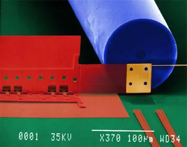
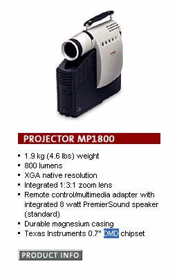

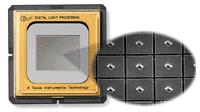
8 Optical Application Optical switches Digital Light Processing


9 Inkjet nozzles Step1 - Nucleation Ink-filled chambers are heated by tiny resistive heating elements Step2 - Bubble Growth By heating the liquid ink a bubble is generated Step3 - Drop Ejection The vaporized part of the ink is propelled towards the paper in a tiny droplet Step4 - Refill Chambers are filled again by the ink through microscopic channels
10 MEMS applications Commercial Biomedical sensors Drug delivery systems Neurological disorders Telecom optical fiber switching Monitoring structural health Automotive safety Military Biochemical warfare detection Inertial systems for guidance and navigation
11 U.S. MEMS markets Year Automotive* Medical Informatio tech.&inds** Military Total In $1,000,000 * 80% air bags ** 1998: inkjets 75%, displays 5.4 Updates info:
12 Why MEMS? A MEMS solution is attractive if: A new function Significant cost reduction Both ** Size reduction is seldom sufficient as the sole reason MEMS is justified when: Added value Increased productivity Cost competitiveness (batch process) Revenue and profit

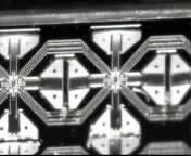
13 MEMS: Evolution from Si IC technology VLSI (FET as an example)

14 Evolution from Si IC technology ocamac/newsletters/newsletter%209/april96_5of6.html oemagazine.com/fromthemagazine/ may01/mems.html lectures/history/history_computing.html asci/mems.html

15 Photolithography

16 IC - Jack Kilby After proving that integrated circuits were possible (1958), I headed teams that built the first military systems and the first computer incorporating integrated circuits. I also worked on teams that invented the handheld calculator and the thermal printer, which was used in portable data terminals.

17 Moore's Law Gordon Moore (co-founder of Intel) predicted in 1965 that the transistor density of semiconductor chips would double roughly every 18 months.


18 Main IC Benefits High quality materials (SC silicon, GaAs) CAD Possessing infrastructure Batch processes
19 MEMS History Original technology was very similar; same materials (silicon), similar processing (photolithography) but different applications: Pressure sensors, accelerometers Silicon for MEMS SC (integration with VLSI) Extensive experience Piezo-resistive High quality material available Infrastructure available mechanically strong
20 MEMS vs IC Some Issues are relevant to both IC and MEMS design: Stress, selective etching, Pattern transfer, cleanliness, structure release. Some are unique: wet environment, 3D, moving parts. Integration requires considering limitations of both technologies. MEMS evolved and now use various materials, processes for a wide range of applications:


21 MEMS Today Gripper end 8 µm Nikolas Chronis and Luke P. Lee, MEMS2004

22 Standard MEMS sensors/actuators Piezo-resistors Comb drives Thermal expansion Surface chemistry
23 MEMS today Materials: SC (Si,GaAs,SiGe), Glass, Silicone. Application: Bio, RF, Chemistry, Optical, Mechanical. Physics/engineering: Elasticity, piezoresistivity, surface properties, capacitive actuators Processes: Bulk machining, surface machining, DRIE, LIGA, Polymers
24 Functionality Transducer Converts energy from one form to another Sensors (Transducers) A device that detects or measures Actuator
25 SiO2/Quartz/glass The stable oxide is one of the key elements for the success of silicon in IC Excellent thermal and electrical insulation Sacrificial layers in surface micromachining processes (selectively etched in HF)
26 Relevant Material Properties Electrical (SC, metals, insulators) Mechanical (elasticity) Thermal (Heat conductivity) Chemical, electro-chemical Biological (bio-compatibility) Optical (roughness) Processing
27 MEMS and materials Mechanical (elasticity) Processing Chemical, electro-chemical Thermal (Heat conductivity) Cost Optical (roughness) Biological (bio-compatibility) Electrical (SC, metals, insulators)
28 Silicon* One of very few materials that can be economically manufactured in single crystal substrates Diamond lattice * Not to be confused with silicone
29 Silicon

30 Czochralski Crystal Growth Process

31 Float zone pulling

32 Silicon boules

33 Silicon 1. Crystal Growth Polysilicon Seed crystal Crucible 6. Edge Rounding Heater 7. Lapping 2. Single Crystal Ingot 8. Wafer Etching 3. Crystal Trimming and Diameter Grind Slurr y Polishing head 4. Flat Grinding 9. Polishing Polishing table 5. Wafer Slicing 10. Wafer Inspection
34 Silicon Summary Properties: Extensive studies and documentation Suitable for electronic, mechanical, thermal, and optical integration Can sustain harsh (mechanical) handling conditions Crystalline: mechanical properties are uniform across wafer lots Structure: Crystalline, Polycrystalline-polysilicon amorphous Conductivity: Semiconductor
35 Silicon Mechanical: Hard and brittle material, deforms elastically, robust Tensile yield strength 7 GPa Maintain mechanical integrity up to 500 C. >500 C plastic deformation. Properties independent of doping (stress when impurities reach 1020 cm -3 ) Polycrystalline and amorphous: properties vary with deposition conditions, but similar to crystalline silicon. Polycrystalline and amorphous: high levels of intrinsic stress, requires annealing (>900 C). Polycrystalline and amorphous: unstable, >250 C.
36 Silicon Fabrication: Crystalline: Wafers Polysilicon: thin film deposition Amorpous : thin film deposition Optics: Not an active optical material (indirect band gap) Transparent at IR <0.4 µm reflects 60% of incedent light Chemistry/biology Stable and resistant (brake fluid, biological medium) Suitable for high purity gases Benign in the body, does not release toxic substances. Cost: Low ultra pure electronic grade silicon wafers are available for IC
37 SiO 2 SiO 2 Silica Fused silica is a purer version of Fused quartz that is made synthetically from various Silicon gasses. 17 crystalline phases Quartz single crystal material, low impurity concentration Fused quartz is the amorphous form of quartz. Fused quartz is made from natural crystalline quartz, usually quartz sand that has been mined. Glass - amorphous solid, impurities, low melting temperature Borosilicate glass is an "Engineered" glass developed specifically for use in environments such as laboratories and heating applications where Thermal, mechanical and chemical conditions are too much for standard, household type glass. Some common names are Pyrex by Corning, and Duran by Schott Glass. Like most glasses, the dominant component of Borosilicate glass is SiO2 with boron and various other elements added to give it its excellent qualities.
38 SiO 2 Properties Color table (Sze) Fabrication Thermally grown by oxidizing silicon at temperature > 800 C. Spin on glass Bonding Mechanical High stress (difficult to control or anneal) limited use as beams or membranes Uses Cost
39 Metals Aluminum Basic electrical interconnections (common and easy to deposit) Non-corrosive environment only T < 300 C (melting temperature =? ) Good light reflector (visible light) Gold/ titanium/tungsten Better for higher temperature Harsher environments Gold is good light reflector in the IR Platinum and palladium Stable for electrochemistry
40 Common Metals in MEMS Metal Ag Al Au Cr, Ti, TiW Cu ITO Ir, Pt W ρ (10-6 Ω cm) , 42, , Applications Electrochemistry Elect interconnects Optical reflection High T elect interconnect Optical refl IR electrochemistry Intermediate adhesion layer Elect interconnects Transparent interconnects Electrochemistry Bio-potential sensors High T elect interconnects Maluf table 2.3, 24
41 Polymers Properties Spin coated with varying thickness; few nm hundreds of microns Used in sensing of chemical gases and humidity Used as Photoresists, SU8: Epoxy based photoresist can form layers up to 100 µm Polyimide Fabrication Spin-on,molding Cost Low
42 Thermal conductivity Material At 300K (W/m K) Convection W/m 2 K Si (SCS) 156 Si 3 N SiO W Al Au Water Air
43 Thermal Expansion Material At 300K (10-6 / C) Si (SCS) Si N SiO W Al
44 Processing Bulk machining vs surface machining Etching, selective etching, sacrificial layers, isotropic vs anisotropic Release processes Deposition processes
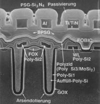
45 Si Etching HF:HNO 3 :CH 3 COOH KOH Ethylene diamine pyrochatechol (EDP) (CH 3 ) 4 NOH (TMAH) SF 6 SF 6 /C 4 F 8 (DRIE) Type Wet Wet Wet Wet Plasma Plasma Anisotropic No Yes Yes Yes varies Yes Rate (µm/min) {111}/{100} selectivity None 100:1 35:1 50:1 None None Nitride etch Low <1 0.1 < SiO 2 etch (nm/min) < P ++ etch stop No Yes Yes Yes No No hazard high
 are material")
46 MEMS Processing Processes (geometry/design) are material specific
47 Standard MEMS sensors/actuators Piezo-resistors Comb drives Thermal expansion
48 Standard MEMS Processes Piezo-resistive Pressure sensor

49 Standard MEMS Processes Comb driver

50 Bio-potential electrodes

51 MEMS applications Mechanical Applications: Actuators
52 Micro-fabricated cilia
Mikrosensorer. Microfabrication 1
 Mikrosensorer Microfabrication 1 Literature Introductory MEMS Fabrication and Applications Thomas M. Adams and Richard A. Layton Available as ebook on http://www.lub.lu.se/en/search/lubsearch.html This
Today s Class. Materials for MEMS
 Lecture 2: VLSI-based Fabrication for MEMS: Fundamentals Prasanna S. Gandhi Assistant Professor, Department of Mechanical Engineering, Indian Institute of Technology, Bombay, Recap: Last Class What is
MEMS Fabrication. Beyond Integrated Circuits. MEMS Basic Concepts
 MEMS Fabrication Beyond Integrated Circuits MEMS Basic Concepts Uses integrated circuit fabrication techniques to make mechanical as well as electrical components on a single chip. Small size 1µm 1mm Typically
Czochralski Crystal Growth
 Czochralski Crystal Growth Crystal Pulling Crystal Ingots Shaping and Polishing 300 mm wafer 1 2 Advantage of larger diameter wafers Wafer area larger Chip area larger 3 4 Large-Diameter Wafer Handling
Fabrication Technology
 Fabrication Technology By B.G.Balagangadhar Department of Electronics and Communication Ghousia College of Engineering, Ramanagaram 1 OUTLINE Introduction Why Silicon The purity of Silicon Czochralski
EE 5611 Introduction to Microelectronic Technologies Fall Tuesday, September 04, 2012 Lecture 01
 EE 5611 Introduction to Microelectronic Technologies Fall 2012 Tuesday, September 04, 2012 Lecture 01 1 Instructor: Jing Bai Contact Email: jingbai@d.umn.edu, hone: (218)726-8606, Office: MWAH 255 Webpage:
EE 5611 Introduction to Microelectronic Technologies Fall Tuesday, September 02, 2014 Lecture 01
 EE 5611 Introduction to Microelectronic Technologies Fall 2014 Tuesday, September 02, 2014 Lecture 01 1 Instructor: Jing Bai Contact Email: jingbai@d.umn.edu, hone: (218)726-8606, Office: MWAH 255 Webpage:
EECS130 Integrated Circuit Devices
 EECS130 Integrated Circuit Devices Professor Ali Javey 9/13/2007 Fabrication Technology Lecture 1 Silicon Device Fabrication Technology Over 10 15 transistors (or 100,000 for every person in the world)
Manufacturing Technologies for MEMS and SMART SENSORS
 4 Manufacturing Technologies for MEMS and SMART SENSORS Dr. H. K. Verma Distinguished Professor (EEE) Sharda University, Greater Noida (Formerly: Deputy Director and Professor of Instrumentation Indian
Preface Preface to First Edition
 Contents Foreword Preface Preface to First Edition xiii xv xix CHAPTER 1 MEMS: A Technology from Lilliput 1 The Promise of Technology 1 What Are MEMS or MST? 2 What Is Micromachining? 3 Applications and
Gaetano L Episcopo. Introduction to MEMS
 Gaetano L Episcopo Introduction to MEMS What are MEMS? Micro Electro Mechanichal Systems MEMS are integrated devices, or systems of devices, with microscopic parts, such as: Mechanical Parts Electrical
L5: Micromachining processes 1/7 01/22/02
 97.577 L5: Micromachining processes 1/7 01/22/02 5: Micromachining technology Top-down approaches to building large (relative to an atom or even a transistor) structures. 5.1 Bulk Micromachining A bulk
Chapter 2 OVERVIEW OF MEMS
 6 Chapter 2 OVERVIEW OF MEMS 2.1 MEMS and Microsystems The term MEMS is an abbreviation of microelectromechanical system. MEMS contains components ofsizes in 1 micrometer to 1 millimeter. The core element
Chapter 3 Silicon Device Fabrication Technology
 Chapter 3 Silicon Device Fabrication Technology Over 10 15 transistors (or 100,000 for every person in the world) are manufactured every year. VLSI (Very Large Scale Integration) ULSI (Ultra Large Scale
Figure 2.3 (cont., p. 60) (e) Block diagram of Pentium 4 processor with 42 million transistors (2000). [Courtesy Intel Corporation.
 (e) Block diagram of Pentium 4 processor with 42 million transistors (2000). [Courtesy Intel Corporation.") Figure 2.1 (p. 58) Basic fabrication steps in the silicon planar process: (a) oxide formation, (b) selective oxide removal, (c) deposition of dopant atoms on wafer, (d) diffusion of dopant atoms into exposed
Figure 2.1 (p. 58) Basic fabrication steps in the silicon planar process: (a) oxide formation, (b) selective oxide removal, (c) deposition of dopant atoms on wafer, (d) diffusion of dopant atoms into exposed
Micro-Electro-Mechanical Systems (MEMS) Fabrication. Special Process Modules for MEMS. Principle of Sensing and Actuation
 Fabrication. Special Process Modules for MEMS. Principle of Sensing and Actuation") Micro-Electro-Mechanical Systems (MEMS) Fabrication Fabrication Considerations Stress-Strain, Thin-film Stress, Stiction Special Process Modules for MEMS Bonding, Cavity Sealing, Deep RIE, Spatial forming
Micro-Electro-Mechanical Systems (MEMS) Fabrication Fabrication Considerations Stress-Strain, Thin-film Stress, Stiction Special Process Modules for MEMS Bonding, Cavity Sealing, Deep RIE, Spatial forming
Thomas M. Adams Richard A. Layton. Introductory MEMS. Fabrication and Applications. Springer
 Thomas M. Adams Richard A. Layton Introductory MEMS Fabrication and Applications Springer Contents Preface xiü Part I Fabrication Chapter 1: Introduction 3 1.1 What are MEMS? 3 1.2 Why MEMS? 4 1.2.1. Low
Physics and Material Science of Semiconductor Nanostructures
 Physics and Material Science of Semiconductor Nanostructures PHYS 570P Prof. Oana Malis Email: omalis@purdue.edu Today Bulk semiconductor growth Single crystal techniques Nanostructure fabrication Epitaxial
Fabrication Technology, Part II
 EEL5225: Principles of MEMS Transducers (Fall 2003) Fabrication Technology, Part II Agenda: Process Examples TI Micromirror fabrication process SCREAM CMOS-MEMS processes Wafer Bonding LIGA Reading: Senturia,
PHYS 534 (Fall 2008) Process Integration OUTLINE. Examples of PROCESS FLOW SEQUENCES. >Surface-Micromachined Beam
 Process Integration OUTLINE. Examples of PROCESS FLOW SEQUENCES. >Surface-Micromachined Beam") PHYS 534 (Fall 2008) Process Integration Srikar Vengallatore, McGill University 1 OUTLINE Examples of PROCESS FLOW SEQUENCES >Semiconductor diode >Surface-Micromachined Beam Critical Issues in Process
PHYS 534 (Fall 2008) Process Integration Srikar Vengallatore, McGill University 1 OUTLINE Examples of PROCESS FLOW SEQUENCES >Semiconductor diode >Surface-Micromachined Beam Critical Issues in Process
Lecture #18 Fabrication OUTLINE
 Transistors on a Chip Lecture #18 Fabrication OUTLINE IC Fabrication Technology Introduction the task at hand Doping Oxidation Thin-film deposition Lithography Etch Lithography trends Plasma processing
Micro-Electro-Mechanical Systems (MEMS) Fabrication. Special Process Modules for MEMS. Principle of Sensing and Actuation
 Fabrication. Special Process Modules for MEMS. Principle of Sensing and Actuation") Micro-Electro-Mechanical Systems (MEMS) Fabrication Fabrication Considerations Stress-Strain, Thin-film Stress, Stiction Special Process Modules for MEMS Bonding, Cavity Sealing, Deep RIE, Spatial forming
Micro-Electro-Mechanical Systems (MEMS) Fabrication Fabrication Considerations Stress-Strain, Thin-film Stress, Stiction Special Process Modules for MEMS Bonding, Cavity Sealing, Deep RIE, Spatial forming
Solid State Sensors. Microfabrication 8/22/08 and 8/25/08
 Solid State Sensors Microfabrication 8/22/08 and 8/25/08 Purpose of This Material To introduce the student to microfabrication techniques as used to fabricate MEMS Sensors Understand concepts not specifics
IC/MEMS Fabrication - Outline. Fabrication
 IC/MEMS Fabrication - Outline Fabrication overview Materials Wafer fabrication The Cycle: Deposition Lithography Etching Fabrication IC Fabrication Deposition Spin Casting PVD physical vapor deposition
Semiconductor device fabrication
 REVIEW Semiconductor device fabrication is the process used to create the integrated circuits (silicon chips) that are present in everyday electrical and electronic devices. It is a multiplestep sequence
CS/ECE 5710/6710. N-type Transistor. N-type from the top. Diffusion Mask. Polysilicon Mask. CMOS Processing
 CS/ECE 5710/6710 CMOS Processing Addison-Wesley N-type Transistor D G +Vgs + Vds S N-type from the top i electrons - Diffusion Mask Mask for just the diffused regions Top view shows patterns that make
VLSI INTRODUCTION P.VIDYA SAGAR ( ASSOCIATE PROFESSOR) Department of Electronics and Communication Engineering, VBIT
 Department of Electronics and Communication Engineering, VBIT") VLSI INTRODUCTION P.VIDYA SAGAR ( ASSOCIATE PROFESSOR) contents UNIT I INTRODUCTION: Introduction to IC Technology MOS, PMOS, NMOS, CMOS & BiCMOS technologies. BASIC ELECTRICAL PROPERTIES : Basic Electrical
VLSI INTRODUCTION P.VIDYA SAGAR ( ASSOCIATE PROFESSOR) contents UNIT I INTRODUCTION: Introduction to IC Technology MOS, PMOS, NMOS, CMOS & BiCMOS technologies. BASIC ELECTRICAL PROPERTIES : Basic Electrical
Crystal Growth and Wafer Fabrication. K.Sivasankaran, Assistant Professor (Senior), VLSI Division, School of Electronics Engineering, VIT
, VLSI Division, School of Electronics Engineering, VIT") Crystal Growth and Wafer Fabrication K.Sivasankaran, Assistant Professor (Senior), VLSI Division, School of Electronics Engineering, VIT Crystal growth Obtaining sand Raw Polysilicon Czochralski Process
Crystal Growth and Wafer Fabrication K.Sivasankaran, Assistant Professor (Senior), VLSI Division, School of Electronics Engineering, VIT Crystal growth Obtaining sand Raw Polysilicon Czochralski Process
Chapter 2 Crystal Growth and Wafer Preparation
 Chapter 2 Crystal Growth and Wafer Preparation Professor Paul K. Chu Advantages of Si over Ge Si has a larger bandgap (1.1 ev for Si versus 0.66 ev for Ge) Si devices can operate at a higher temperature
EE40 Lec 22. IC Fabrication Technology. Prof. Nathan Cheung 11/19/2009
 Suggested Reading EE40 Lec 22 IC Fabrication Technology Prof. Nathan Cheung 11/19/2009 300mm Fab Tour http://www-03.ibm.com/technology/manufacturing/technology_tour_300mm_foundry.html Overview of IC Technology
There are basically two approaches for bulk micromachining of. silicon, wet and dry. Wet bulk micromachining is usually carried out
 57 Chapter 3 Fabrication of Accelerometer 3.1 Introduction There are basically two approaches for bulk micromachining of silicon, wet and dry. Wet bulk micromachining is usually carried out using anisotropic
Lecture 19 Microfabrication 4/1/03 Prof. Andy Neureuther
 EECS 40 Spring 2003 Lecture 19 Microfabrication 4/1/03 Prof. ndy Neureuther How are Integrated Circuits made? Silicon wafers Oxide formation by growth or deposition Other films Pattern transfer by lithography
Surface micromachining and Process flow part 1
 Surface micromachining and Process flow part 1 Identify the basic steps of a generic surface micromachining process Identify the critical requirements needed to create a MEMS using surface micromachining
Surface Micromachining
 Surface Micromachining Micro Actuators, Sensors, Systems Group University of Illinois at Urbana-Champaign Outline Definition of surface micromachining Most common surface micromachining materials - polysilicon
Microfabrication of Integrated Circuits
 Microfabrication of Integrated Circuits OUTLINE History Basic Processes Implant; Oxidation; Photolithography; Masks Layout and Process Flow Device Cross Section Evolution Lecture 38, 12/05/05 Reading This
Complexity of IC Metallization. Early 21 st Century IC Technology
 EECS 42 Introduction to Digital Electronics Lecture # 25 Microfabrication Handout of This Lecture. Today: how are Integrated Circuits made? Silicon wafers Oxide formation by growth or deposition Other
ME 189 Microsystems Design and Manufacture. Chapter 9. Micromanufacturing
 ME 189 Microsystems Design and Manufacture Chapter 9 Micromanufacturing This chapter will offer an overview of the application of the various fabrication techniques described in Chapter 8 in the manufacturing
INF5490 RF MEMS. LN02: MEMS Fabrication. Spring 2012, Oddvar Søråsen Department of Informatics, UoO
 INF5490 RF MEMS LN02: MEMS Fabrication Spring 2012, Oddvar Søråsen Department of Informatics, UoO 1 Micromachining Today s lecture Important process steps General Summary: MEMS-specific steps Examples
A discussion of crystal growth, lithography, etching, doping, and device structures is presented in
 Chapter 5 PROCESSING OF DEVICES A discussion of crystal growth, lithography, etching, doping, and device structures is presented in the following overview gures. SEMICONDUCTOR DEVICE PROCESSING: AN OVERVIEW
Chapter 2 Manufacturing Process
 Digital Integrated Circuits A Design Perspective Chapter 2 Manufacturing Process 1 CMOS Process 2 CMOS Process (n-well) Both NMOS and PMOS must be built in the same silicon material. PMOS in n-well NMOS
Mostafa Soliman, Ph.D. May 5 th 2014
 Mostafa Soliman, Ph.D. May 5 th 2014 Mostafa Soliman, Ph.D. 1 Basic MEMS Processes Front-End Processes Back-End Processes 2 Mostafa Soliman, Ph.D. Wafers Deposition Lithography Etch Chips 1- Si Substrate
ELEC 3908, Physical Electronics, Lecture 4. Basic Integrated Circuit Processing
 ELEC 3908, Physical Electronics, Lecture 4 Basic Integrated Circuit Processing Lecture Outline Details of the physical structure of devices will be very important in developing models for electrical behavior
PROCESSING OF INTEGRATED CIRCUITS
 PROCESSING OF INTEGRATED CIRCUITS Overview of IC Processing (Part I) Silicon Processing Lithography Layer Processes Use in IC Fabrication (Part II) Integrating the Fabrication Steps IC Packaging (Part
Fabrication Process. Crystal Growth Doping Deposition Patterning Lithography Oxidation Ion Implementation CONCORDIA VLSI DESIGN LAB
 Fabrication Process Crystal Growth Doping Deposition Patterning Lithography Oxidation Ion Implementation 1 Fabrication- CMOS Process Starting Material Preparation 1. Produce Metallurgical Grade Silicon
Fabrication and Layout
 ECEN454 Digital Integrated Circuit Design Fabrication and Layout ECEN 454 3.1 A Glimpse at MOS Device Polysilicon Aluminum ECEN 475 4.2 1 Material Classification Insulators Glass, diamond, silicon oxide
MEMS Devices. Fraunhofer Institute for Silicon Technology ISIT. Itzehoe, Germa. any
 Examples of CMP Processess for the Manufacturing of MEMS Devices Gerfried Zwicke er Fraunhofer Institute for Silicon Technology ISIT Itzehoe, Germa any gerfried.zwicker@isit.fraunhofer.de Contents MEMS
General Introduction to Microstructure Technology p. 1 What is Microstructure Technology? p. 1 From Microstructure Technology to Microsystems
 General Introduction to Microstructure Technology p. 1 What is Microstructure Technology? p. 1 From Microstructure Technology to Microsystems Technology p. 9 The Parallels to Microelectronics p. 15 The
Chapter 3 CMOS processing technology
 Chapter 3 CMOS processing technology (How to make a CMOS?) Si + impurity acceptors(p-type) donors (n-type) p-type + n-type => pn junction (I-V) 3.1.1 (Wafer) Wafer = A disk of silicon (0.25 mm - 1 mm thick),
R Sensor resistance (Ω) ρ Specific resistivity of bulk Silicon (Ω cm) d Diameter of measuring point (cm)
 ρ Specific resistivity of bulk Silicon (Ω cm) d Diameter of measuring point (cm)") 4 Silicon Temperature Sensors 4.1 Introduction The KTY temperature sensor developed by Infineon Technologies is based on the principle of the Spreading Resistance. The expression Spreading Resistance derives
4 Silicon Temperature Sensors 4.1 Introduction The KTY temperature sensor developed by Infineon Technologies is based on the principle of the Spreading Resistance. The expression Spreading Resistance derives
Evolution of MEMS Technology
 Evolution of MEMS Technology 1 Raksha Sahadev Hukkeri, 2 Shreya Madapurmath, 3 Shreelekha Navale 1,2,3 UG Student, Department of ECE, SDMCET Dharwad Abstract Micro-Electro-Mechanical Systems (MEMS) is
EE 5344 Introduction to MEMS. CHAPTER 3 Conventional Si Processing
 3. Conventional licon Processing Micromachining, Microfabrication. EE 5344 Introduction to MEMS CHAPTER 3 Conventional Processing Why silicon? Abundant, cheap, easy to process. licon planar Integrated
Silicon Manufacturing
 Silicon Manufacturing Group Members Young Soon Song Nghia Nguyen Kei Wong Eyad Fanous Hanna Kim Steven Hsu th Fundamental Processing Steps 1.Silicon Manufacturing a) Czochralski method. b) Wafer Manufacturing
Microstructure of Electronic Materials. Amorphous materials. Single-Crystal Material. Professor N Cheung, U.C. Berkeley
 Microstructure of Electronic Materials Amorphous materials Single-Crystal Material 1 The Si Atom The Si Crystal diamond structure High-performance semiconductor devices require defect-free crystals 2 Crystallographic
CHAPTER - 4 CMOS PROCESSING TECHNOLOGY
 CHAPTER - 4 CMOS PROCESSING TECHNOLOGY Samir kamal Spring 2018 4.1 CHAPTER OBJECTIVES 1. Introduce the CMOS designer to the technology that is responsible for the semiconductor devices that might be designed
4. Process Integration: Case Studies
 Case Study #2: FCantilevered Microgripper Surface Machined MEMS Case Study #2: FCantilevered Microgripper Sandia Lucent Sandia Integrated Accelerometers Optomechanical Systems Integrated Sensors 1 Bulk
Lecture 5. SOI Micromachining. SOI MUMPs. SOI Micromachining. Silicon-on-Insulator Microstructures. Agenda:
 EEL6935 Advanced MEMS (Spring 2005) Instructor: Dr. Huikai Xie SOI Micromachining Agenda: SOI Micromachining SOI MUMPs Multi-level structures Lecture 5 Silicon-on-Insulator Microstructures Single-crystal
Lecture 10: MultiUser MEMS Process (MUMPS)
") MEMS: Fabrication Lecture 10: MultiUser MEMS Process (MUMPS) Prasanna S. Gandhi Assistant Professor, Department of Mechanical Engineering, Indian Institute of Technology, Bombay, 1 Recap Various VLSI based
MEMS: Fabrication Lecture 10: MultiUser MEMS Process (MUMPS) Prasanna S. Gandhi Assistant Professor, Department of Mechanical Engineering, Indian Institute of Technology, Bombay, 1 Recap Various VLSI based
PY2N20 Material Properties and Phase Diagrams
 PY2N20 Material Properties and Phase Diagrams Lecture 9 P. Stamenov, PhD School of Physics, TCD PY2N20-9 Semiconductor Wafer Production - Si Czochralski Growth Growth from melt Melt 99.999999% pure polycrystalline
Semiconductor Manufacturing Process 10/11/2005
 Semiconductor Manufacturing Process 10/11/2005 Photolithography Oxidation CVD PVD Photolithography The purpose of photolithography is to imprint the desired pattern of a micro component on a substrate,
The Physical Structure (NMOS)
") The Physical Structure (NMOS) Al SiO2 Field Oxide Gate oxide S n+ Polysilicon Gate Al SiO2 SiO2 D n+ L channel P Substrate Field Oxide contact Metal (S) n+ (G) L W n+ (D) Poly 1 3D Perspective 2 3 Fabrication
The Physical Structure (NMOS) Al SiO2 Field Oxide Gate oxide S n+ Polysilicon Gate Al SiO2 SiO2 D n+ L channel P Substrate Field Oxide contact Metal (S) n+ (G) L W n+ (D) Poly 1 3D Perspective 2 3 Fabrication
VLSI Digital Systems Design
 VLSI Digital Systems Design CMOS Processing cmpe222_03process_ppt.ppt 1 Si Purification Chemical purification of Si Zone refined Induction furnace Si ingot melted in localized zone Molten zone moved from
EE C245 ME C218 Introduction to MEMS Design Fall 2007
 EE C245 ME C218 Introduction to MEMS Design Fall 2007 Prof. Clark T.-C. Nguyen Dept. of Electrical Engineering & Computer Sciences University of California at Berkeley Berkeley, CA 94720 Lecture 10: Bulk
Welcome MNT Conference 1 Albuquerque, NM - May 2010
 Welcome MNT Conference 1 Albuquerque, NM - May 2010 Introduction to Design Outline What is MEMs Design General Considerations Application Packaging Process Flow What s available Sandia SUMMiT Overview
Tutorial on Micro Electro Mechanical Systems (MEMS)
") Tutorial on Micro Electro Mechanical Systems (MEMS) Bruce Kim Department of Electrical, 1 ! What is MEMS! Why MEMS! Applications! MEMS Fabrication! MEMS Packaging! Conclusion MEMS 2 WHAT IS MEMS! MEMS
Tutorial on Micro Electro Mechanical Systems (MEMS) Bruce Kim Department of Electrical, 1 ! What is MEMS! Why MEMS! Applications! MEMS Fabrication! MEMS Packaging! Conclusion MEMS 2 WHAT IS MEMS! MEMS
Micromachining vs. Soft Fabrication
 Introduction to BioMEMS & Medical Microdevices Silicon Microfabrication Part 1 Companion lecture to the textbook: Fundamentals of BioMEMS and Medical Microdevices, by Prof., http://saliterman.umn.edu/
Micromachining AMT 2505
 Micromachining AMT 2505 Shanmuga Raja.B (BVB0912004) Module leader : Mr. Raja Hussain Introduction Micromachining are inherently connected to the evolution of Micro Electro Mechanical Systems (MEMS). Decades
This Appendix discusses the main IC fabrication processes.
 IC Fabrication B B.1 Introduction This Appendix discusses the main IC fabrication processes. B.2 NMOS fabrication NMOS transistors are formed in a p-type substrate. The NMOS fabrication process requires
SURFACE MICROMACHINING
 SURFACE MICROMACHINING Features are built up, layer by layer on the surface of a substrate. Surface micromachined devices are much smaller than bulk micromachined components. Nature of deposition process
6.777J/2.732J Design and Fabrication of Microelectromechanical Devices Spring Term Solution to Problem Set 2 (16 pts)
") 6.777J/2.732J Design and Fabrication of Microelectromechanical Devices Spring Term 2007 By Brian Taff (Adapted from work by Feras Eid) Solution to Problem Set 2 (16 pts) Issued: Lecture 4 Due: Lecture
6.777J/2.732J Design and Fabrication of Microelectromechanical Devices Spring Term 2007 By Brian Taff (Adapted from work by Feras Eid) Solution to Problem Set 2 (16 pts) Issued: Lecture 4 Due: Lecture
Microfabrication of Heterogeneous, Optimized Compliant Mechanisms SUNFEST 2001 Luo Chen Advisor: Professor G.K. Ananthasuresh
 Microfabrication of Heterogeneous, Optimized Compliant Mechanisms SUNFEST 2001 Luo Chen Advisor: Professor G.K. Ananthasuresh Fig. 1. Single-material Heatuator with selective doping on one arm (G.K. Ananthasuresh)
INTEGRATED-CIRCUIT TECHNOLOGY
 INTEGRATED-CIRCUIT TECHNOLOGY 0. Silicon crystal growth and wafer preparation 1. Processing Steps 1.1. Photolitography 1.2. Oxidation 1.3. Layer Deposition 1.4. Etching 1.5. Diffusion 1.6 Backend: assembly,
VLSI Design and Simulation
 VLSI Design and Simulation CMOS Processing Technology Topics CMOS Processing Technology Semiconductor Processing How do we make a transistor? Fabrication Process Wafer Processing Silicon single crystal
Making of a Chip Illustrations
 Making of a Chip Illustrations 22nm 3D/Trigate Transistors Version April 2015 1 The illustrations on the following foils are low resolution images that visually support the explanations of the individual
EE 330 Lecture 8. IC Fabrication Technology Part II. - Oxidation - Epitaxy - Polysilicon - Interconnects
 EE 330 Lecture 8 IC Fabrication Technology Part II - Oxidation - Epitaxy - Polysilicon - Interconnects Review from Last Time MOS Transistor Bulk Source Gate Drain p-channel MOSFET Lightly-doped n-type
EE 330 Lecture 9. IC Fabrication Technology Part II. -Oxidation -Epitaxy -Polysilicon -Planarization -Resistance and Capacitance in Interconnects
 EE 330 Lecture 9 IC Fabrication Technology Part II -Oxidation -Epitaxy -Polysilicon -Planarization -Resistance and Capacitance in Interconnects Review from Last Time IC Fabrication Technology Crystal Preparation
Surface Micromachining
 Surface Micromachining Outline Introduction Material often used in surface micromachining Material selection criteria in surface micromachining Case study: Fabrication of electrostatic motor Major issues
EE 330 Lecture 9. IC Fabrication Technology Part 2
 EE 330 Lecture 9 IC Fabrication Technology Part 2 Quiz 8 A 2m silicon crystal is cut into wafers using a wire saw. If the wire diameter is 220um and the wafer thickness is 350um, how many wafers will this
Lecture 7 CMOS MEMS. CMOS MEMS Processes. CMOS MEMS Processes. Why CMOS-MEMS? Agenda: CMOS MEMS: Fabrication. MEMS structures can be made
 EEL6935 Advanced MEMS (Spring 2005) Instructor: Dr. Huikai Xie CMOS MEMS Agenda: Lecture 7 CMOS MEMS: Fabrication Pre-CMOS Intra-CMOS Post-CMOS Deposition Etching Why CMOS-MEMS? Smart on-chip CMOS circuitry
CHAPTER 1 HOW SEMICONDUCTOR CHIPS ARE MADE
 CHAPTER 1 HOW SEMICONDUCTOR CHIPS ARE MADE Hwaiyu Geng Hewlett-Packard Company Palo Alto, California Lin Zhou Intel Corporation Hillsboro, Oregon 1.1 INTRODUCTION Over the past decades, an information
EFFECT OF CRYSTALORIENTATIONIN OXIDATION PROCESS OF VLSI FABRICATION
 International Journal of Research in Engineering, Technology and Science, Volume VII, Special Issue, Feb 2017 www.ijrets.com, editor@ijrets.com, ISSN 2454-1915 EFFECT OF CRYSTALORIENTATIONIN OXIDATION
PROCESS FLOW AN INSIGHT INTO CMOS FABRICATION PROCESS
 Contents: VI Sem ECE 06EC63: Analog and Mixed Mode VLSI Design PROCESS FLOW AN INSIGHT INTO CMOS FABRICATION PROCESS 1. Introduction 2. CMOS Fabrication 3. Simplified View of Fabrication Process 3.1 Alternative
CMOS Manufacturing process. Design rule set
 CMOS Manufacturing process Circuit design Set of optical masks Fabrication process Circuit designer Design rule set Process engineer All material: Chap. 2 of J. Rabaey, A. Chandrakasan, B. Nikolic, Digital
Supporting Information
 Supporting Information Fast-Response, Sensitivitive and Low-Powered Chemosensors by Fusing Nanostructured Porous Thin Film and IDEs-Microheater Chip Zhengfei Dai,, Lei Xu,#,, Guotao Duan *,, Tie Li *,,
Silicon Microfabrication Part 2
 Introduction to BioMEMS & Medical Microdevices Silicon Microfabrication Part 2 Companion lecture to the textbook: Fundamentals of BioMEMS and Medical Microdevices, by Prof., http://saliterman.umn.edu/
Overview. Silicon Microfabrication Part 2. Introduction to BioMEMS & Medical Microdevices
 Introduction to BioMEMS & Medical Microdevices Silicon Microfabrication Part 2 Companion lecture to the textbook: Fundamentals of BioMEMS and Medical Microdevices, by Prof., http://saliterman.umn.edu/
Microelectronics Devices
 Microelectronics Devices Yao-Joe Yang 1 Outline Basic semiconductor physics Semiconductor devices Resistors Capacitors P-N diodes BJT/MOSFET 2 Type of Solid Materials Solid materials may be classified
KGC SCIENTIFIC Making of a Chip
 KGC SCIENTIFIC www.kgcscientific.com Making of a Chip FROM THE SAND TO THE PACKAGE, A DIAGRAM TO UNDERSTAND HOW CPU IS MADE? Sand CPU CHAIN ANALYSIS OF SEMICONDUCTOR Material for manufacturing process
PHYSICAL ELECTRONICS(ECE3540) Brook Abegaz, Tennessee Technological University, Fall 2013
 Brook Abegaz, Tennessee Technological University, Fall 2013") PHYSICAL ELECTRONICS(ECE3540) Brook Abegaz, Tennessee Technological University, Fall 2013 1 Chapter 1 The Crystal Structure of Solids Physical Electronics: Includes aspects of the physics of electron movement
PHYSICAL ELECTRONICS(ECE3540) Brook Abegaz, Tennessee Technological University, Fall 2013 1 Chapter 1 The Crystal Structure of Solids Physical Electronics: Includes aspects of the physics of electron movement
Fabrication Technology, Part I
 EEL5225: Principles of MEMS Transducers (Fall 2003) Fabrication Technology, Part I Agenda: Oxidation, layer deposition (last lecture) Lithography Pattern Transfer (etching) Impurity Doping Reading: Senturia,
Instructor: Dr. M. Razaghi. Silicon Oxidation
 SILICON OXIDATION Silicon Oxidation Many different kinds of thin films are used to fabricate discrete devices and integrated circuits. Including: Thermal oxides Dielectric layers Polycrystalline silicon
Dr. Lynn Fuller Webpage:
 ROCHESTER INSTITUTE OF TECHNOLOGY MICROELECTRONIC ENGINEERING Microelectromechanical Systems (MEMs) Process Integration Dr. Lynn Fuller Webpage: http://people.rit.edu/lffeee 82 Lomb Memorial Drive Rochester,
Lecture 0: Introduction
 Lecture 0: Introduction Introduction Integrated circuits: many transistors on one chip. Very Large Scale Integration (VLSI): bucketloads! Complementary Metal Oxide Semiconductor Fast, cheap, low power
EE6303 LINEAR INTEGRATED CIRCUITS AND APPLICATIONS 2 MARK QUESTIONS WITH ANSWERS UNIT I IC FABRICATION
 SRI VENKATESWARA COLLEGE OF ENGINEERING AND TECHNOLOGY TIRUPACHUR DEPARTMENT OFELECTRICAL AND ELECTRONICS ENGINEERING EE6303 LINEAR INTEGRATED CIRCUITS AND APPLICATIONS 1. Define an Integrated circuit.
Silver Diffusion Bonding and Layer Transfer of Lithium Niobate to Silicon
 Chapter 5 Silver Diffusion Bonding and Layer Transfer of Lithium Niobate to Silicon 5.1 Introduction In this chapter, we discuss a method of metallic bonding between two deposited silver layers. A diffusion
3. Photolithography, patterning and doping techniques. KNU Seminar Course 2015 Robert Mroczyński
 3. Photolithography, patterning and doping techniques KNU Seminar Course 2015 Robert Mroczyński Critical technology processes Photolithography The aim of this process is to transfer (in the most accurate
Ultrasonic Micromachining in the fabrication of MEMS Micro-sensors
 Ultrasonic Micromachining in the fabrication of MEMS Micro-sensors Jamil Akhtar Professor AcSIR New Delhi Chief Scientist & Head, CSIR-CEERI, Pilani, INDIA CEERI, Pilani A constituent laboratory of CSIR,
TOWARD MEMS!Instructor: Riadh W. Y. Habash
 TOWARD MEMS!Instructor: Riadh W. Y. Habash Students are presented with aspects of general production and manufacturing of integrated circuit (IC) products to enable them to better liaise with and participate
Most semiconductor devices contain at least one junction between p-type and n-type material. These p-n junctions are fundamental to the performance
 Ch. 5: p-n Junction Most semiconductor devices contain at least one junction between p-type and n-type material. These p-n junctions are fundamental to the performance of functions such as rectification,
Change in stoichiometry
 Measurement of Gas Sensor Performance Gas sensing materials: 1. Sputtered ZnO film (150 nm (Massachusetts Institute of Technology) 2. Sputtered SnO 2 film (60 nm) (Fraunhofer Institute of Physical Measurement