Radioisotope Batteries. Jake Blanchard University of Wisconsin April 2010
|
|
|
- Harry Stone
- 6 years ago
- Views:
Transcription

1 Radioisotope Batteries Jake Blanchard University of Wisconsin April 2010
2 Introduction Radioisotope batteries provide reliable batteries with high energy density They are valuable when long life is needed and recharging or refueling is difficult Many of the conversion technologies can function in harsh environments They can be very useful as onboard MEMS power sources
3 Applications Long-lived cell phone batteries Self-powered sensors on automobiles Self-powered sensors in humans Sensors for tracking animals Building/bridge sensors MEMS Micro-robots Smart Dust Networks
4 Caveats Cost Safety/regulation Shielding is generally simple Concern is with breakage of packaging Security is also an issue
5 Radioisotopes Alpha emitters release energetic He nuclei typically at 4-6 MeV per particle Beta emitters emit electrons or positrons (and neutrinos or antineutrinos) energy spectrum Gamma emitters emit electromagnetic radiation penetrating - undesirable
6 Isotope Selection Type of radiation Alpha Beta Half-Life Long - Long battery life (238-Pu 0.6 W/g, 86 yr half life) Short - Higher power density (210-Po 137 W/g, 3 month half-life) Avoid gammas in the decay chain (safety) Watch out for (alpha, n) reactions and Brehmstrahlung Watch particle range, displacement damage, and cost
7 Radioisotopes and decay N M X a-decay 4 2He N-4 M-2 Y N M X b-decay e - N M-1Y n e Isotope Average energy Half life Specific activity Specific Power Power Density (KeV) (year) (Ci/g) (W/g) (W/cc) 63-Ni H Sr/ 200/930 29/2 d Y 210-Po Pu Cm

8 Beta Spectra (E in MeV)
9 What is a Nuclear Battery? Goal: convert energy from radioactive decay to electricity Options: Direct charge collection Indirect (scintillation) Betavoltaic Thermoelectric Thermionic thermophotovoltaic
10 Comparison Consider 1 mg for power source Source Energy Content (mw-hr) Chemical Battery (Li-ion) 0.3 Fuel Cell (methanol, 50%) Po (5% - 4 years) H (5% - 4 years) 500
11
12 Direct conversion nuclear battery Collector Radioisotope High voltage Direct conversion nuclear battery: collecting charges emitted from radioisotopes with a capacitor to achieve high voltage output (J. H. Coleman, 1953) V Q C kv voltages can be created in vacuum
13 Static Accumulation Early 1950 s Source at K D is electrical insulator Chamber is evacuated 0.25 Ci Sr kv About 1 na 0.2 mw Linder, Rappaport, Loferski
14 Adding a Dielectric Early 1950 s Source at S D is dielectric; C is collector Radiation penetrates dielectric No need for vacuum High voltage Prevents secondary electrons from getting back to source 50 mci Sr-90 polystyrene 7 kv Keller et al
15 Secondary Collector Use beta source MgO used to maximize secondary s Collector is graphite coated Al 1e-5 mm Hg vacuum Shorr
16 Contact Potential Ionize gas between two plates Dissimilar plates will develop potential due to differing work functions Low efficiency (low absorption coefficient) and high ionization energy (30 ev) Operates at 1-2 V Shorr

 Regulators nervous about tracking Pu")

17 Pacemakers 3 Ci Pu-238 ~3 ounces, ~3 inches <mw power levels 100 mrem/y to patient Since supplanted by Li batteries (~10 yr life) Regulators nervous about tracking Pu Thermoelectric (some betacell concepts)
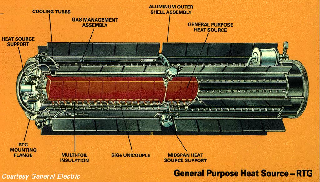
18 Radioisotope Thermoelectric Generators (RTGs) Used in many NASA missions Use radoisotope (usually ceramic Pu-238) to provide heat Electricity produced by thermoelectric No moving parts 41 have been flown by US Fuel: 2.7 kg. 133 kci Power: 276 W Power (11 years): 216 W Total Weight: 56 kg Lifetime: over 20 years Dimensions: D=42 cm, L=114 cm
19


20 Heating Units NASA s RHU 33 Ci Power is 1 W 1.4 oz. 1 cubic inch 2.7 g of Pu-238 (oxide form) Rugged, reliable

21 A Compact Thermoelectric John H. Glenn Research Center, Cleveland, Ohio Hi-Z Technology and JPL 40 mw electric power 240 cm 3, 300 g total weight

 I p V oc P max 0.25mCi 1mCi 0.71nA 2.")
 obtained/ - No performance degradation after 1 year Second")

22 Current (na) Betavoltaic Microbattereis First type: planar Si pn-diode with electroplated 63 Ni DIP package Electroplated 63 Ni thin film Leads Glass PN-diode Voltage (mv) I p V oc P max 0.25mCi 1mCi 0.71nA 2.41nA 64mW 115mV 0.04nW 0.24nW - Nanopower( 0.04~0.24nW) obtained/ - No performance degradation after 1 year Second type: inverted pyramid array Si pn-diode P N Glass - Area magnification: 1.85 / nW (128mV/2.86nA) obtained 63 NiCl/HCI solution (8 Ci/ l) Efficiency:0.03~0.1% ~10 times > micromachined RTG

23 Scaling of Power Currently 1mCi of 63 Ni is used Source density of~ mci/mm 2 leads to 2~8 nw/cm 2 10mCi~100mCi of 63 Ni is expected to be used Source density is ~1~2 mci/mm 2 100nW ~200 nw can be obtained Gives 100~200 nw/cm 2 Energy conversion efficiency of 0.5~1% is expected to be achieved Theoretical conversion efficiency: 3~5%
24 Current (A) Using Radioisotope 147 Pm Another way to raise power output : using high energy power source Pm, with E avg = 62 kev and E max = 220 kev and half-life of 2.6 year is also a promising pure beta source for microbattery. Preliminary Results P N 147 Pm SiO 2-1.E-23-1 m of SiO 2 is used as protection layer - Device area : 2mm 3mm - 5mCi of 147 Pm is used - test result : Is= 140nA, Voc=183mV, Pmax = 16.8nW - Conversion efficiency: 0.62% - long-term stability is under test E-08-8.E-08-1.E-07 Voltage (V)


25 Porous Silicon Try to maximize area exposed to source
26 Thin, Flexible Semiconductors For low energy beta emitters, source layers must be thin (sub-micron) Range of particles in semiconductor is also a few microns at most Hence, thin semiconductors are an advantage Multi-layer devices can offer good power density with good efficiency
 MCNP (with diode) chord method 0.6 0.5 0.4 0.3 0 0.2 0.4 0.6 0.8 1 1.")
27 2-sided escape probability Self-Absorption Ni-63 and Si MCNP (no diode) MCNP (with diode) chord method source thickness (microns)
28
29 Silicon Carbide Wide Bandgap semiconductors offer hope for larger efficiencies Simulations indicate on the order of 25% conversion efficiency

30 A New Concept
 Initial")
: 10.")
31 Distance ( m) Self reciprocating cantilever 30 Experimental data Calculated values Time (minute) Initial gap (d 0 ): 33 m Period: 6 min. 8 sec. Residual charges: C Peak force (kd 0 ): 10.1 N Assumed Collection efficiency (a): 10%
 The cantilever is made of low")

32 Distance ( m) Self-reciprocating SiN cantilever Blue: measured deflection Red: signal from the Wheatstone bridge Time (s) The cantilever is made of low stress SiN thin film with dimensions 500 m 300 m 1.7 m. The cantilever is mounted on a DIP package for wire bonding. Four poly resistors form a Wheatstone bridge to measure the deflection of the cantilever. The signal from the Wheatstone bridge is sent to an instrumentation amplifier and then output from the amplifier is measured.
33 Voltage (V) Self-powered Sensor/Actuator/Transmitter Time ( s) PZT Au electrodes C 1 C 2 To oscilloscope Nickel-63 source (a) ε C 3 PZT To oscilloscope dv I C1 dt (b) Nickel-63 source C 4 C 1 C 2 C 3
34 Bottom Line Market is applications which can justify cost and risk of using radioisotope fuels Advantage is very long life
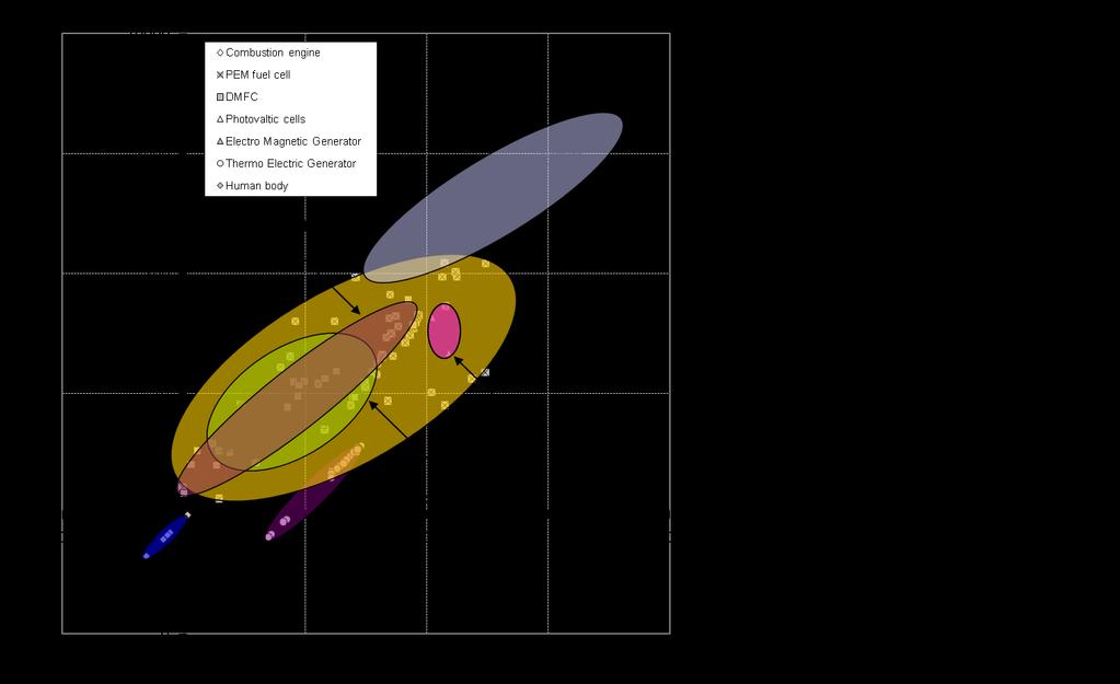
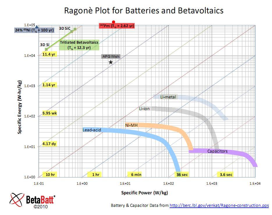
35 Comparing Technologies
Atomic battery From Wikipedia, the free encyclopedia
 Page 1 of 5 Atomic battery From Wikipedia, the free encyclopedia The terms atomic battery, nuclear battery, tritium battery and radioisotope generator are used to describe a device which uses energy from
BY AMIT LAL & JAMES BLANCHARD
 +NUCLEAR BATTERIES THE DAINTIEST DYNAMOS BY HARVESTING ENERGY FROM RADIOACTIVE SPECKS, NUCLEAR MICROBATTERIES COULD POWER TOMORROW S MICROELECTROMECHANICAL MARVELS AND MAYBE YOUR CELLPHONE, TOO BY AMIT
ELECTRICAL RESISTIVITY AS A FUNCTION OF TEMPERATURE
 ELECTRICAL RESISTIVITY AS A FUNCTION OF TEMPERATURE Introduction The ability of materials to conduct electric charge gives us the means to invent an amazing array of electrical and electronic devices,
Space Power, Thermoelectrics, and Thermionics
 Space Power, Thermoelectrics, and Thermionics 2014 Workshop on Thermionic Energy Conversion for Space and Earth NASA Johnson Space Center Houston, TX Jean-Pierre Fleurial Jet Propulsion Laboratory/California
Supporting Information
 Supporting Information Fast-Response, Sensitivitive and Low-Powered Chemosensors by Fusing Nanostructured Porous Thin Film and IDEs-Microheater Chip Zhengfei Dai,, Lei Xu,#,, Guotao Duan *,, Tie Li *,,
PRINCIPLES OF OPERATION
 A dose calibrators is an integral part of any nuclear medicine department. This tutorial focuses on the main principles of operation and all of the issues related to quality control testing of this equipment;
Betavoltaics: An Innovative Power Source Enabling Next Generation Low-Power Sensor and Communication Devices
 CAPT JT Elder, USN Commanding Officer NSWC Crane Betavoltaics: An Innovative Power Source Enabling Next Generation Low-Power Sensor and Communication Devices Dr. Adam Razavian, SES Technical Director NSWC
Neutron Detector development at the ILL Based on 3 He and alternative convertors
 Neutron Detector development at the ILL Based on 3 He and alternative convertors Bruno Guerard Basic principles of 3He neutron gas detectors outline The golden age of 3 He detectors (~2000 20) shown with
National Semiconductor LM2672 Simple Switcher Voltage Regulator
 Construction Analysis National Semiconductor LM2672 Simple Switcher Voltage Regulator Report Number: SCA 9712-570 Global Semiconductor Industry the Serving Since 1964 17350 N. Hartford Drive Scottsdale,
Solar Cells and Photosensors.
 Designing Photonic Crystals in Strongly Absorbing Material for Applications in Solar Cells and Photosensors. Minda Wagenmaker 1, Ebuka S. Arinze 2, Botong Qiu 2, Susanna M. Thon 2 1 Mechanical Engineering
Fabrication Technology
 Fabrication Technology By B.G.Balagangadhar Department of Electronics and Communication Ghousia College of Engineering, Ramanagaram 1 OUTLINE Introduction Why Silicon The purity of Silicon Czochralski
Electron Emission. The reader is familiar with the current conduction (i.e. flow of electrons) through a conductor. 28 Principles of Electronics
 through a conductor. 28 Principles of Electronics") 28 Principles of Electronics 2 Electron Emission 2.1 Electron Emission 2.2 Types of Electron Emission 2.3 Thermionic Emission 2.4 Thermionic Emitter 2.5 Commonly Used Thermionic Emitters 2.6 Cathode Construction
28 Principles of Electronics 2 Electron Emission 2.1 Electron Emission 2.2 Types of Electron Emission 2.3 Thermionic Emission 2.4 Thermionic Emitter 2.5 Commonly Used Thermionic Emitters 2.6 Cathode Construction
Cal-Chip Electronics, Incorporated Thick Film Chip Resistors - RM Series
 Thick Film Chip Resistors - RM Series Fixed Chip Resistors manufactured for more compact electronic components and automatic mounting system. These Chip Resistors have electrical stability and mechanical
UTILIZATION OF ATMOSPHERIC PLASMA SURFACE PREPARATION TO IMPROVE COPPER PLATING PROCESSES.
 SESSION 14 MATERIALS AND PROCESSES FOR ADVANCED PACKAGING UTILIZATION OF ATMOSPHERIC PLASMA SURFACE PREPARATION TO IMPROVE COPPER PLATING PROCESSES. Eric Schulte 1, Gilbert Lecarpentier 2 SETNA Corporation
Metallization deposition and etching. Material mainly taken from Campbell, UCCS
 Metallization deposition and etching Material mainly taken from Campbell, UCCS Application Metallization is back-end processing Metals used are aluminum and copper Mainly involves deposition and etching,
Radiation Shielding Glass RD 30 RD 50
 Radiation Shielding Glass RD 30 RD 50 2 SCHOTT is a leading international technology group in the areas of specialty glass and glass-ceramics. With more than 130 years of outstanding development, materials
Preprint - Mechatronics 2008, Le Grand-Bornand, France, May
 Potentialities of piezoresistive cantilever force sensors based on free standing thick films Hélène Debéda(*), Isabelle Dufour, Patrick Ginet, Claude Lucat University of Bordeaux 1, IMS Laboratory, 51
Thin Films: Sputtering Systems (Jaeger Ch 6 & Ruska Ch 7,) Can deposit any material on any substrate (in principal) Start with pumping down to high
 Can deposit any material on any substrate (in principal) Start with pumping down to high") Thin Films: Sputtering Systems (Jaeger Ch 6 & Ruska Ch 7,) Can deposit any material on any substrate (in principal) Start with pumping down to high vacuum ~10-7 torr Removes residual gases eg oxygen from
Thin Films: Sputtering Systems (Jaeger Ch 6 & Ruska Ch 7,) Can deposit any material on any substrate (in principal) Start with pumping down to high vacuum ~10-7 torr Removes residual gases eg oxygen from
Growth Of TiO 2 Films By RF Magnetron Sputtering Studies On The Structural And Optical Properties
 Journal of Multidisciplinary Engineering Science and Technology (JMEST) Growth Of TiO 2 Films By RF Magnetron Sputtering Studies On The Structural And Optical Properties Ahmed K. Abbas 1, Mohammed K. Khalaf
Packaging Technologies for SiC Power Modules
 Packaging Technologies for SiC Power Modules Masafumi Horio Yuji Iizuka Yoshinari Ikeda ABSTRACT Wide bandgap materials such as silicon carbide (SiC) and gallium nitride (GaN) are attracting attention
Question Bank. Producing and Using Stream of Electrons
 Producing and Using Stream of Electrons 1. (a) What do you understand by the following terms : (i) Free electrons, (ii) Thermions? (b) State one way by which thermions differ from free electrons. Ans.(a)
Lecture Day 2 Deposition
 Deposition Lecture Day 2 Deposition PVD - Physical Vapor Deposition E-beam Evaporation Thermal Evaporation (wire feed vs boat) Sputtering CVD - Chemical Vapor Deposition PECVD LPCVD MVD ALD MBE Plating
Surface micromachining and Process flow part 1
 Surface micromachining and Process flow part 1 Identify the basic steps of a generic surface micromachining process Identify the critical requirements needed to create a MEMS using surface micromachining
High-sensitivity Silicon Resonant Strain Sensor
 High-sensitivity Silicon Resonant Strain Sensor Takeru Samejima *1 Yoshitaka Suzuki *1 Nobuyuki Hamamatsu *1 Hiroshi Yokouchi *1 Takashi Yoshida *1 Silicon resonant sensors, which are used in the DPharp
Reduction of Backscattered Radiation in Enclosure X-ray Radiography
 Abstract Reduction of Backscattered Radiation in Enclosure X-ray Radiography Samir Abdul-Majid, Abdulrahim Kinsara, Abdullah Almasoumi and Mohamed Kallothody Faculty of Engineering, King Abdulaziz University
Topics Relevant to CdTe Thin Film Solar Cells
 Topics Relevant to CdTe Thin Film Solar Cells March 13, 2012 The University of Toledo, Department of Physics and Astronomy SSARE, PVIC Principles and Varieties of Solar Energy (PHYS 4400) and Fundamentals
Development of Piezoelectric Nanocomposites for Energy Harvesting and Self-Sensing
 Development of Piezoelectric Nanocomposites for Energy Harvesting and Self- Kenneth J. Loh Assistant Professor Department of Civil & Environmental Engineering University of California, Davis The Applied
Proceedings Post Fabrication Processing of Foundry MEMS Structures Exhibiting Large, Out-of-Plane Deflections
 Proceedings Post Fabrication Processing of Foundry MEMS Structures Exhibiting Large, Out-of-Plane Deflections LaVern Starman 1, *, John Walton 1, Harris Hall 1 and Robert Lake 2 1 Sensors Directorate,
Thin Films: Sputtering Systems (Jaeger Ch 6 & Ruska Ch 7,) Sputtering: gas plasma transfers atoms from target to substrate Can deposit any material
 Sputtering: gas plasma transfers atoms from target to substrate Can deposit any material") Thin Films: Sputtering Systems (Jaeger Ch 6 & Ruska Ch 7,) Sputtering: gas plasma transfers atoms from target to substrate Can deposit any material on any substrate (in principal) Start with pumping down
Thin Films: Sputtering Systems (Jaeger Ch 6 & Ruska Ch 7,) Sputtering: gas plasma transfers atoms from target to substrate Can deposit any material on any substrate (in principal) Start with pumping down
HIGH TEMPERATURE CERAMIC & GRAPHITE ADHESIVES
 HIGH TEMPERATURE & GRAPHITE S Technical Bulletin A2 Ceramabond 835-M bonds halogen lamp. Ceramabond 503 coats heater used to 1700 ºC. Ceramabond 685-N bonds infrared heater. Graphi-Bond 551-RN bonds graphite
Applications of High-Performance MEMS Pressure Sensors Based on Dissolved Wafer Process
 Applications of High-Performance MEMS Pressure Sensors Based on Dissolved Wafer Process Srinivas Tadigadapa and Sonbol Massoud-Ansari Integrated Sensing Systems (ISSYS) Inc., 387 Airport Industrial Drive,
Overall Conclusions and Future Projections OVERALL CONCLUSIONS
 OVERALL CONCLUSIONS This article brings the thesis to a close by presenting the conclusions drawn from the outcome of the radiation effects on the structural and optical properties of heavy metal oxide
High-energy x-ray production with pyroelectric crystals
 JOURNAL OF APPLIED PHYSICS 97, 104916 2005 High-energy x-ray production with pyroelectric crystals Jeffrey A. Geuther a and Yaron Danon Department of Mechanical, Aerospace, and Nuclear Engineering, Rensselaer
DEPOSITION OF THIN FILMS ON POLYCARBONATES BY PULSE DIELECTRIC BARRIER DISCHARGE
 a DEPOSITION OF THIN FILMS ON POLYCARBONATES BY PULSE DIELECTRIC BARRIER DISCHARGE T. Opalińska a, B. Ulejczyk a, L. Karpiński b, K. Schmidt-Szałowski c a) Industrial Chemistry Research Institute, Rydygiera
Surface Micromachining
 Surface Micromachining Outline Introduction Material often used in surface micromachining Material selection criteria in surface micromachining Case study: Fabrication of electrostatic motor Major issues
Transmission Electron Microscopy (TEM) Prof.Dr.Figen KAYA
 Prof.Dr.Figen KAYA") Transmission Electron Microscopy (TEM) Prof.Dr.Figen KAYA Transmission Electron Microscope A transmission electron microscope, similar to a transmission light microscope, has the following components along
Transmission Electron Microscopy (TEM) Prof.Dr.Figen KAYA Transmission Electron Microscope A transmission electron microscope, similar to a transmission light microscope, has the following components along
Nuclear Power in Space
 Nuclear Power in Space Zara Hodgson 9 th International School on Nuclear Power, Warsaw, Poland 16 th November 2017 Introduction Zara Hodgson Chemical Engineer with over 15 years in nuclear Lead NNL s Research
When external forces are
 The Strain Gage 2 FORCE-RELATED MEASUREMENTS The Strain Gage Sensor Designs Measuring Circuits Application & Installation W When external forces are applied to a stationary object, stress and strain are
AC : MICROWAVE PLASMA CLEANER DESIGN FOR SEMI- CONDUCTOR FABRICATION AND MATERIALS PROCESSING LABO- RATORY USE
 AC 2011-2416: MICROWAVE PLASMA CLEANER DESIGN FOR SEMI- CONDUCTOR FABRICATION AND MATERIALS PROCESSING LABO- RATORY USE Mustafa G. Guvench, University of Southern Maine Mustafa G. Guvench received M.S.
Long-term reliability of SiC devices. Power and Hybrid
 Long-term reliability of SiC devices Power and Hybrid Rob Coleman Business Development and Applications Manager TT electronics, Power and Hybrid Roger Tall Product Specialist Charcroft Electronics Ltd
Producing Molybdenum-99 in CANDU Reactors. Jerry M Cuttler Cuttler & Associates Inc. Abstract
 31 st Annual Conference of the Canadian Nuclear Society, Montréal, Québec, 2010 May 24-27 Producing Molybdenum-99 in CANDU Reactors Jerry M Cuttler Cuttler & Associates Inc Abstract This paper discusses
NanoSystemsEngineering: NanoNose Final Status, March 2011
 1 NanoSystemsEngineering: NanoNose Final Status, March 2011 The Nanonose project is based on four research projects (VCSELs, 3D nanolithography, coatings and system integration). Below, the major achievements
X-ray Photoelectron Spectroscopy
 X-ray Photoelectron Spectroscopy X-ray photoelectron spectroscopy (XPS) is a non-destructive technique used to analyze the elemental compositions, chemical and electronic states of materials. XPS has a
Chemistry 145 Exam number 4 name 11/19/98 # Faraday s constant is 96,500 c/mole of electrons.
 Chemistry 145 Exam number 4 name 11/19/98 # Faraday s constant is 96,500 c/mole of electrons. A.(16) An electrochemical cell is prepared with a strip of manganese metal dipping in to a 1.0 M MnSO 4 solution
Production of PV cells
 Production of PV cells MWp 1400 1200 Average market growth 1981-2003: 32% 2004: 67% 1000 800 600 400 200 0 1991 1992 1993 1994 1995 1996 1997 1998 1999 2000 2001 2002 2003 2004 rest 1.0 1.0 1.0 2.0 4.0
PRODUCTION OF COBALT-60 IN PARR-1/KANUPP (CANDU) Mushtaq Ahmad Isotope Production Division, PINSTECH, Islamabad
 Mushtaq Ahmad Isotope Production Division, PINSTECH, Islamabad") PRODUCTION OF COBALT-60 IN PARR-1/KANUPP (CANDU) Mushtaq Ahmad Isotope Production Division, PINSTECH, Islamabad COBALT-60 Cobalt is a metal element with only one stable isotope: cobalt-59. When natural
PRODUCTION OF COBALT-60 IN PARR-1/KANUPP (CANDU) Mushtaq Ahmad Isotope Production Division, PINSTECH, Islamabad COBALT-60 Cobalt is a metal element with only one stable isotope: cobalt-59. When natural
Plutonium-238 and the Radioisotope Power Systems Supply Chain Office of Nuclear Energy
 Plutonium-238 and the Radioisotope Power Systems Supply Chain Office of Nuclear Energy Tracey Bishop Deputy Assistant Secretary for Nuclear Energy U.S. Department of Energy February 27, 2017 What are Radioisotope
LIGHTWEIGHT, LIGHT-TRAPPED, THIN GaAs SOLAR CELL FOR SPACECRAFT APPLICATIONS: PROGRESS AND RESULTS UPDATE' ABSTRACT INTRODUCTION
 LIGHTWEIGHT, LIGHT-TRAPPED, THIN GaAs SOLAR CELL FOR SPACECRAFT APPLICATIONS: PROGRESS AND RESULTS UPDATE' M.H. Hannon, M.W. Dashiell, L.C. DiNetta, and A.M. Barnett AstroPower, Inc. Newark, DE 1971 6-2000
R Sensor resistance (Ω) ρ Specific resistivity of bulk Silicon (Ω cm) d Diameter of measuring point (cm)
 ρ Specific resistivity of bulk Silicon (Ω cm) d Diameter of measuring point (cm)") 4 Silicon Temperature Sensors 4.1 Introduction The KTY temperature sensor developed by Infineon Technologies is based on the principle of the Spreading Resistance. The expression Spreading Resistance derives
4 Silicon Temperature Sensors 4.1 Introduction The KTY temperature sensor developed by Infineon Technologies is based on the principle of the Spreading Resistance. The expression Spreading Resistance derives
Sampling for Airborne Radioactivity
 Sampling for Airborne Radioactivity Peter D. Harty Human Protection and Performance Division Defence Science and Technology Organisation DSTO-TN-0782 ABSTRACT This report examines how to sample airborne
Energy From Electron Transfer. Chemistry in Context
 Energy From Electron Transfer Chemistry in Context Energy Types Batteries Hybrid Cars (Electrical) H 2 (and Other) Fuel Cells Solar Fuel Cell Car Demo H 2 Fuel Cell Reactions Step 1: H 2 (g) 2H + (aq)
Modeling of MEMS Based Bolometer for Measuring Radiations from Nuclear Power Plant
 Modeling of MEMS Based Bolometer for Measuring Radiations from Nuclear Power Plant S. Nisitha* 1, T. Satyanarayana #2, S. Sreeja 1 1 B. Tech 2 M.Sc., M. Phil., Ph.D *NPMASS Centre, Department of EIE, Lakireddy
Aluminum Nitride Thin Films for High Frequency Smart Ultrasonic Sensor Systems
 18th World Conference on Nondestructive Testing, 16-20 April 2012, Durban, South Africa Aluminum Nitride Thin Films for High Frequency Smart Ultrasonic Sensor Systems Thomas HERZOG, Susan WALTER, Susanne
Sensor. Device that converts a non-electrical physical or chemical quantity into an electrical signal. Sensor Processor Display Output signal
 Microsensors Outline Sensor & microsensor Force and pressure microsensors Position and speed microsensors Acceleration microsensors Chemical microsensors Biosensors Temperature sensors Sensor Device that
bans the use of lead, mercury, cadmium, hexavalent chromium and polybrominated biphenyls (PBB) or polybrominated diphenyl ethers (PBDE).
 or polybrominated diphenyl ethers (PBDE).") MS7907 PRESSURE SENSOR DIE (0-7 BAR) 0 to 700 kpa range (7 bar or 102 PSI) Absolute/differential pressure sensors High linearity, small size RoHS-compatible & Pb-free 1 DESCRIPTION The sensor element of
MS7907 PRESSURE SENSOR DIE (0-7 BAR) 0 to 700 kpa range (7 bar or 102 PSI) Absolute/differential pressure sensors High linearity, small size RoHS-compatible & Pb-free 1 DESCRIPTION The sensor element of
Meteorology 432. Thermometry Spring 2013
 Meteorology 432 Thermometry Spring 2013 General Temperature impacts every day life. Errors of 2-3 ºC are not uncommon in many networks. Bank thermometers or Car thermometers. Errors of this magnitude are
nicrom e l e c t r o n i c
 G E N E R A L High Performance Thick Film Resistors C A T A L O G 3 Nicrom Electronic Via Roncaglia CH - 6883 Novazzano SWITZERLAND Phone : ++4 () 9 68 99 86 Fax : ++4 () 9 68 99 86 info@nicrom-electronic.com
Oxide Growth. 1. Introduction
 Oxide Growth 1. Introduction Development of high-quality silicon dioxide (SiO2) has helped to establish the dominance of silicon in the production of commercial integrated circuits. Among all the various
Case Study Power Electronics Cleaning - Solvent to ph Neutral: Enhancing Safety, Process Efficiency and Productivity
 Case Study Power Electronics Cleaning - Solvent to ph Neutral: Enhancing Safety, Process Efficiency and Productivity Ravi Parthasarathy, M.S.Ch.E. Senior Application Engineer ZESTRON Americas Outline Introduction
APPLICATIONS OF ELECTROCHEMISTRY
 APPLICATIONS OF ELECTROCHEMISTRY SPONTANEOUS REDOX REACTIONS APPLICATIONS OF ELECTROCHEMICAL CELLS BATTERIES A galvanic cell, or series of combined galvanic cells, that can be used as a source of direct
ME 189 Microsystems Design and Manufacture. Chapter 9. Micromanufacturing
 ME 189 Microsystems Design and Manufacture Chapter 9 Micromanufacturing This chapter will offer an overview of the application of the various fabrication techniques described in Chapter 8 in the manufacturing
S2 RANGER LE: Analysis of Light Elements in Cement, Slags and Feldspar
 S2 RANGER LE: Analysis of Light Elements in Cement, Slags and Feldspar 1 Welcome Today s topics: S2 RANGER LE o o o Overview XFlash LE detector Improved X-ray tube Analysis of Light Elements in Cement
Project III. 4: THIN FILM DEVICES FOR LARGE AREA ELECTRONICS
 Project III. 4: THIN FILM DEVICES FOR LARGE AREA ELECTRONICS Project leader: Dr D.N. Kouvatsos Collaborating researchers from other projects: Dr D. Davazoglou Ph.D. candidates: M. Exarchos, L. Michalas
Ceramic Microchannel Devices for Thermal Management. C. Lewinsohn, J. Fellows, and H. Anderson Ceramatec, Inc. Salt Lake City, UT
 Ceramic Microchannel Devices for Thermal Management C. Lewinsohn, J. Fellows, and H. Anderson Ceramatec, Inc. Salt Lake City, UT The Right Size for The Right Physics centi milli micro 2 Multiscale Structure
EVERGREEN: IMPROVING THE LIFETIME OF PLASTIC SCINTILLATORS
 EVERGREEN: IMPROVING THE LIFETIME OF PLASTIC SCINTILLATORS Mike Kusner and Peter Menge Saint-Gobain Crystals, Hiram Ohio USA BACKGROUND: Thousands of plastic scintillators are deployed outdoors where they
A novel measuring system for the metrological characterization of piezoresistive films at high temperature
 P1.1 A novel measuring system for the metrological characterization of piezoresistive films at high temperature Damiano Crescini, and Marco Romani Dipartimento di Elettronica per l'automazione Facoltà
Rockwell R RF to IF Down Converter
 Construction Analysis Rockwell R6732-13 RF to IF Down Converter Report Number: SCA 9709-552 Global Semiconductor Industry the Serving Since 1964 17350 N. Hartford Drive Scottsdale, AZ 85255 Phone: 602-515-9780
3.46 OPTICAL AND OPTOELECTRONIC MATERIALS
 Badgap Engineering: Precise Control of Emission Wavelength Wavelength Division Multiplexing Fiber Transmission Window Optical Amplification Spectrum Design and Fabrication of emitters and detectors Composition
Novel Solutions for ESD Sensitive Devices
 Novel Solutions for ESD Sensitive Devices Chris Schreiber Magnecomp cschreiber@magnecomp.com Safely Dissipating ESD Problem Static Charging is created by either Tribocharging or Induction and the uncontrolled
Physics 171, Physics and Society Quiz 1 1pm Thurs Sept 14, 2017 Each question has one correct answer, or none (choose e on the clicker). 1.
. 1.") Physics 171, Physics and Society Quiz 1 1pm Thurs Sept 14, 2017 Each question has one correct answer, or none (choose e on the clicker). 1. Maria is riding her bicycle on a flat road at 10 mi/hr. Then
Physics 171, Physics and Society Quiz 1 1pm Thurs Sept 14, 2017 Each question has one correct answer, or none (choose e on the clicker). 1. Maria is riding her bicycle on a flat road at 10 mi/hr. Then
Study on Properties of Silicon Oxycarbide Thin Films Prepared by RF Magnetron Sputtering Tao Chen a, Maojin Dong, Jizhou Wang,Ling Zhang and Chen Li
 Study on Properties of Silicon Oxycarbide Thin Films Prepared by RF Magnetron Sputtering Tao Chen a, Maojin Dong, Jizhou Wang,Ling Zhang and Chen Li Science and Technology on Surface Engineering Laboratory,
Cadmium Oxide Nano Particles by Sol-Gel and Vapour- Liquid-Solid Methods
 Nano Vision, Vol.1 (1), 47-53 (2011) Cadmium Oxide Nano Particles by Sol-Gel and Vapour- Liquid-Solid Methods S. SAKTHIVEL* and D. MANGALARAJ 1 *PG and Research Department of Physics, Rajah Serfoji Govt.
II. NEG THIN FILM DEPOSITION
 Deposition of Non-Evaporable Getter Thin Films and Vacuum Pumping Performances Ankit Sur Engineering Department, Wayne State University, Detroit, MI 48202 The ERL (Energy Recovery Linac) proposed at Cornell
In-situ Heating Characterisation Using EBSD
 Webinar In-situ Heating Characterisation Using EBSD Speakers Dr. Ali Gholinia Dr. Neil Othen Dr. Jenny Goulden Topics Introduction to EBSD Why do in-situ experiments? EBSD equipment requirements for in-situ
Ultra High Barrier Coatings by PECVD
 Society of Vacuum Coaters 2014 Technical Conference Presentation Ultra High Barrier Coatings by PECVD John Madocks & Phong Ngo, General Plasma Inc., 546 E. 25 th Street, Tucson, Arizona, USA Abstract Silicon
Micro-Electro-Mechanical Systems (MEMS) Fabrication. Special Process Modules for MEMS. Principle of Sensing and Actuation
 Fabrication. Special Process Modules for MEMS. Principle of Sensing and Actuation") Micro-Electro-Mechanical Systems (MEMS) Fabrication Fabrication Considerations Stress-Strain, Thin-film Stress, Stiction Special Process Modules for MEMS Bonding, Cavity Sealing, Deep RIE, Spatial forming
Micro-Electro-Mechanical Systems (MEMS) Fabrication Fabrication Considerations Stress-Strain, Thin-film Stress, Stiction Special Process Modules for MEMS Bonding, Cavity Sealing, Deep RIE, Spatial forming
Planning for the Decontamination of the Plutonium Fuel Form (PuFF) Facility Savannah River Site (SRS), South Carolina
 Facility Savannah River Site (SRS), South Carolina") Planning for the Decontamination of the Plutonium Fuel Form (PuFF) Facility Savannah River Site (SRS), South Carolina - 10095 Richard J. Abitz, Andrew J. Duncan, Marie C. Kane, Raymond A. Dewberry, Joseph
Planning for the Decontamination of the Plutonium Fuel Form (PuFF) Facility Savannah River Site (SRS), South Carolina - 10095 Richard J. Abitz, Andrew J. Duncan, Marie C. Kane, Raymond A. Dewberry, Joseph
EE-612: Lecture 28: Overview of SOI Technology
 EE-612: Lecture 28: Overview of SOI Technology Mark Lundstrom Electrical and Computer Engineering Purdue University West Lafayette, IN USA Fall 2006 NCN www.nanohub.org Lundstrom EE-612 F06 1 outline 1)
PROCESSING OF INTEGRATED CIRCUITS
 PROCESSING OF INTEGRATED CIRCUITS Overview of IC Processing (Part I) Silicon Processing Lithography Layer Processes Use in IC Fabrication (Part II) Integrating the Fabrication Steps IC Packaging (Part
PROGRESS IN THIN-FILM LENR RESEARCH AT THE UNIVERSITY OF ILLINOIS
 Miley, G.H., et al. Progress in thin-film LENR research at the University of Illinois. in The 9th International Conference on Cold Fusion, Condensed Matter Nuclear Science. 2002. Tsinghua Univ., Beijing,
Ameren Seminar August 19 20, 2008 Effingham, IL
 Ameren Seminar August 19 20, 2008 Effingham, IL ESP Basics By Tom Lugar Buell APC Fisher-Klosterman, Inc. A CECO Environmental Company Fundamentals of Electrostatic Precipitator (ESP) Operation The Process
EMA4303/5305 Electrochemical Engineering Lecture 05 Applications (1)
") EMA4303/5305 Electrochemical Engineering Lecture 05 Applications (1) Prof. Zhe Cheng Mechanical & Materials Engineering Florida International University Corrosion Definition Electrochemical attack of metals
EMA4303/5305 Electrochemical Engineering Lecture 05 Applications (1) Prof. Zhe Cheng Mechanical & Materials Engineering Florida International University Corrosion Definition Electrochemical attack of metals
CMOS Manufacturing process. Circuit designer. Design rule set. Process engineer. Set of optical masks. Fabrication process.
 CMOS Manufacturing process Circuit design Set of optical masks Fabrication process Circuit designer Design rule set Process engineer All material: Chap. 2 of J. Rabaey, A. Chandrakasan, B. Nikolic, Digital
Leveraging the Precision of Electroforming over Alternative Processes When Developing Nano-scale Structures
 VOLUME 4 - ELECTROFORMING Leveraging the Precision of over Alternative Processes When Developing Nano-scale Structures Electrical and mechanical component and subsystem designers generally have five techniques
CONTACT ELECTRICAL CHARACTERISTICS TIGER CLAW CONTACT TESTING. A. Gas Tight
 CONTACT ELECTRICAL CHARACTERISTICS TIGER CLAW CONTACT TESTING A. Gas Tight 1. Purpose - To evaluate the integrity of the contact interface by assessment of the gas tight characteristics of the contacting
Method to obtain TEOS PECVD Silicon Oxide Thick Layers for Optoelectronics devices Application
 Method to obtain TEOS PECVD Silicon Oxide Thick Layers for Optoelectronics devices Application ABSTRACT D. A. P. Bulla and N. I. Morimoto Laboratório de Sistemas Integráveis da EPUSP São Paulo - S.P. -
Transactions on Engineering Sciences vol 2, 1993 WIT Press, ISSN
 A study of thin-film continuous coating process by vapour deposition P. Gimondo," F. Arezzo,* B. Grifoni,* G. Jasch& "Centra Sviluppo Materiali SpA, Via di Castel & Von Ardenne Anlagentchnik GmbH, Plattleite
Physical structure of matter. Monochromatization of molybdenum X-rays X-ray Physics. What you need:
 X-ray Physics Physical structure of matter Monochromatization of molybdenum X-rays What you can learn about Bremsstrahlung Characteristic radiation Energy levels Absorption Absorption edges Interference
3D Miniaturization of optical polarimetric principle used for subcutaneous glucose monitoring
 3D Miniaturization of optical polarimetric principle used for subcutaneous glucose monitoring A. Steinke, H.-J. Freitag, M. Schädel, A. T. Winzer, O. Brodersen, J. Freitag, H.Wünscher Content 0. CiS at
NiP Resistor Manufacturing Overview
 0 NiP Resistor Manufacturing Overview Thin film NiP resistive alloy material is made by electrodepositing of the NiP alloy onto copper foil (RESISTOR-CONDUCTOR MATERIAL) which is then laminated to a dielectric
Amorphous Silicon Solar Cells
 The Birnie Group solar class and website were created with much-appreciated support from the NSF CRCD Program under grants 0203504 and 0509886. Continuing Support from the McLaren Endowment is also greatly
Molybdenum Carbide Nano-Powder for Production of Mo-99 Radionuclides
 World Journal of Nuclear Science and Technology, 2012, 2, 58-63 http://dx.doi.org/10.4236/wjnst.2012.22010 Published Online April 2012 (http://www.scirp.org/journal/wjnst) Molybdenum Carbide Nano-Powder
INTRODUCTION TO ELECTROCHEMISTRY: CURRENT, VOLTAGE, & BATTERIES. Introduction. Electrochemistry Revised 4/28/14
 INTRODUCTION TO ELECTROCHEMISTRY: CURRENT, VOLTAGE, & BATTERIES Introduction Electrochemical Cells In this part of the experiment, four half cells are created by immersing metal strips of zinc, copper,
Scintillating Optical Fibers
 Scintillating Optical Fibers Plastic Scintillating Fibers Saint-Gobain Crystals manufactures a variety of plastic scintillating, wavelength-shifting and light-transmitting fibers used for research and
Features Conductive Room Temperature Cure. Product Ref IP 4525IP Low viscosity adhesive & coating. High thermal conductivity
 Properties and Part Selection Overview Selection Table - Epoxy-Based Adhesive Properties Features Conductive Room Temperature Cure Product Ref 120 132 4461IP 42IP 438 700 Properties High electrical conductivity
X-RAY EMISSION IN THE HIGH-CURRENT GLOW DISCHARGE EXPERIMENTS
 Karabut, A.B. X-ray emission in the high-current glow discharge experiments. in The 9th International Conference on Cold Fusion, Condensed Matter Nuclear Science. 2002. Tsinghua Univ., Beijing, China:
Good Diffraction Practice Webinar Series
 Good Diffraction Practice Webinar Series LYNXEYE XE - Combining 1D Speed with 0D Background June 27 2013 www.bruker-webinars.com Welcome Brian Jones Product Manager - XRD Bruker AXS Inc. Madison, Wisconsin,
SLID bonding for thermal interfaces. Thermal performance. Technology for a better society
 SLID bonding for thermal interfaces Thermal performance Outline Background and motivation The HTPEP project Solid-Liquid Inter-Diffusion (SLID) Au-Sn SLID Cu-Sn SLID Reliability and bond integrity Alternative
Radiation Tolerant Isolation Technology
 Radiation Tolerant Isolation Technology Background The following contains a brief description of isolation technologies used for radiation hardened integrated circuits. The technologies mentioned are junction
Industrial Diamonds: Present and the Future
 M.Sc Miroljub Vilotijevic Dr. Borislav Dacic Industrial Diamonds: Present and the Future Three resorting qualities of diamond available today for industrial use are: natural diamond (i), synthetic diamond