Paradee Leerungnawarat. Department of Materials Science and Engineering
|
|
|
- Cuthbert Lyons
- 6 years ago
- Views:
Transcription
1 Paradee Leerugawarat Departmet of Materials Sciece ad Egieerig
2 Itroductio What is SiC? Why SiC? SiC has may advatages over Si. It is widely used for high power, high temperature electroic devices. Why High-Desity Plasma? It is very difficult to wet etch (practicality). Covetioal Reactive Io Etchig produces very low etch rates


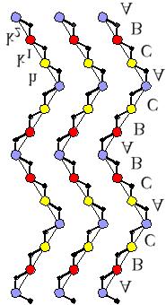
3 Silico Carbide Crystal Structure 3C-SiC 6H-SiC 4H-SiC
4 Silico carbide properties Properties 3C-SiC 6H-SiC 4H-SiC Si Badgap (300 K, ev) Idirect Idirect Idirect Idirect Electro Mobility (cm 2 /V-s) room temperature, dopig~10 16 cm -3 Hole Mobility (cm 2 /V-s) room temperature, dopig~10 16 cm -3 Breakdow field (MV/cm) > dopig~10 16 cm -3 Thermal Coductivity (W/cm-K) room temperature, dopig~10 17 cm -3 Electro drift velocity (10 7 cm/s) Dielectric costat, ε
5 SiC Power Electroics The much wider badgap ad breakdow voltage for SiC relative to Si makes it attractive for high temperature, high power device applicatios. To date, high power MOSFETs, rectifiers, thyristors ad IGBTs have all bee demostrated i SiC, with far superior breakdow voltage ad o-resistace compared to Si. To make may of these devices, it is ecessary to have low damage, dry etch processes with high aisotropy.
6 Theoretical ad Experimetal Performace of SiC Ad Si Schottky Rectifiers.
7 Oe Applicatio: Via-Hole Etchig EMITTER FINGERS GROUNDING PAD 2-4 mil THINNED WAFER VIA FLIP-SIDE PLATED METAL Requiremets: High SiC Etch rate : High selectivity for SiC over mask material
8 Previously Reported Etch rates of SiC Reactor SiC Gas Coditio at highest ER ER Ref (Å-mi -1 ) RIE 6H CHF 3 /O 2 20 sccm, 200 W, 0% O SF 6 /O CF 4 /O NF 3 /O C SF 6 150W, 80 mtorr H,4H NF mtorr, sccm, 275 W ECR 6H CF 4 /O 2 500W, -100V, 17.5%O 2, 50 sccm C,6H CF 4 /O 2 650W, -100 V, 17%O 2, 50sccm H 20SF 6 /10Ar 750W, 250 rf, 2 mtorr, 30 sccm C,6H SF 6 /O W, 1 mtorr, 4 sccm H 10Cl 2 /5Ar 1000W, 150 rf, 1.5 mtorr, 15 sccm Cl 2 /5H W, 150 rf, 1.5 mtorr, 15 sccm IBr/4Ar 1000W, 250 rf, 1.5 mtorr, 15 sccm 1100 NF 3 800W, 100 rf, 1mTorr, 10 sccm 1600 SF 6 800W, 100 rf, 1 mtorr, 10 sccm 450 ICP 6H Cl 2 /Ar or /He 100 Cl 2, 750 W, 250rf, 5 mtorr Cl 2 /Xe 13%Cl 2, 750 W, 250rf, 5 mtorr 260 IBr/Ar 10%Ar, 750 W, 250 rf, 5 mtorr 800 ICl/Ar 66%Ar, 750 W, 250 rf, 5 mtorr 250 6H NF 3 /O 2 or Ar 100%NF 3, 750W, 250 rf, 5mTorr
9 High-Desity Plasma I this work we employ a form of high desity plasma (Iductive Coupled Plasma) ad several differet F 2 -based gas chemistries. HDP provides high io flux, low io eergy ad efficiet plasma dissociatio : low damage, high rate etchig. We examied the active plasma species by Optical Emissio Spectroscopy (OES) i order to uderstad the etch mechaism. We also examied several differet mask materials (Al, ITO ad Ni).
10 ICP Schematic Gas Distributio Plasma Alumia Chamber Sample ~ 2 MHz Power Supply Powered Electrode MHz rf source ~
11 Etchig Mechaisms e i e e i e i i e i s sput acc s s s sput diff abs s s des s abs s des s abs s sput s- Sputterig Chemical Reactio Io-Assisted Plasma Etchig Plasma Regio Substrate By products (Volatile products)
12 Keys to SiC Etchig Must break strog Si-C bods i order to allow etch products to form. Expect SiF x ad CF x to be the etch products (These are much more volatile tha SiCl x ad CCl x, ad hece F 2 - based plasma chemistries are favored over Cl 2 -based chemistries).
13 Experimet 1. 4H-SiC 2. Al 3. Ni 4. ITO Mask with Apiezo wax ICP reactor 2 mtorr 15 sccm Etched depth measuremet Gas : NF 3, BF 3, SF 6 or PF 5 ICP source power: 750, 1000, 1250,1500 W Rf chuck power: 150, 250, 350, 450 W Optical Emissio Spectroscopy (OES) Stylus Profilometer(Tecor) Roughess Measuremet Atomic Force Microscope
14 Etch rate i differet ICP Power i four differet gases PF 5 Etch Rate (Å/mi) BF 3 SF 6 NF 3 250W rf, 2 mtorr, 15 sccm Etch Yield (atom/io) PF 5 BF 3 SF 6 NF 3 250W rf, 2 mtorr, 15 sccm ICP-Power (W)
15 Dissociatio Eergies ad OES Spectra 20 9 Itesity (Arb. U.) NF W ICP 5W rf 35mTorr F F F F F Chemical Bod Stregth (KCal/mol) NF SF Itesity (Arb. U.) 6 3 B 100 BF W ICP 5W rf 35mTorr SiF x F F F F Itesity (Arb. U.) SF W ICP 5W rf 35mTorr SiF x F F PF BF Itesity (Arb. U.) PF W ICP 5W rf 35mTorr P SiF x F F F Wavelegth (m) Wavelegth (m)
16 Etch rate ad dc self-bias i differet rf power 7000 Etch rate (Å/mi) PF 5 BF 3 SF 6 NF PF 5 dc self-bias (-V) BF 3 SF 6 NF 3 750W ICP rf-power (W)

17 Surface roughess data from AFM SiC Cotrol : RMS = 2.5 m PF 5 : RMS = 2.0 m BF 3 : RMS = 0.8 m 1500 W Source Power 250 W rf chuck power 1 miute SF 6 : RMS = 1.4 m NF 3 : RMS = 0.6 m
18 Surface roughess i differece gases RMS (m) Cotrol PF 5 BF 3 SF 6 NF 3 Surface may actually become smoother due to the agular depedece of io millig which leads to faster removal of sharp features o the surface. + 1 θ ER ICP-Power (W) 0 90 θ
19 Etchig i 10SF 6 /5Ar w ad w/o UV Etch Rate (Å/mi) UV w/o UV dc self-bias dc self-bias (-V) Etch Rate (Å/mi) UV w/o UV dc self-bias dc self-bias (-V) ICP power (W) rf power (W)
20 Etchig i 10Cl 2 /5Ar w ad w/o UV Etch Rate (Å/mi) UV w/o UV dc self-bias ICP power (W) dc self-bias (-V) Etch Rate (Å/mi) UV w/o UV dc self-bias rf power (W) dc self-bias (-V)
21 Surface roughess of SiC at 200 W rf chuck power w UV illumiatio w/o UV illumiatio RMS (m) 1.5 RMS (m) w UV illumiatio w/o UV illumiatio ICP power (W) 10SF 6 /5Ar ICP power (W) 10Cl 2 /5Ar

22 SEM: SiC surface, etches with SF 6 W/O UV With UV
23 Etch rate of differet metal masks 10NF 3 /5O W rf chuck power 750 W ICP power 2 2 Etch Rate (µm/mi) 1 0 SiC Al Ni ITO Etch Deposit Etch Rate (µm/mi) 1 0 SiC Al Ni ITO Etch Deposit ICP Power (W) rf Power (W)
24 Etch rate ad selectivity i various gas ratio Etch Rate (µm/mi) Etchig SiC Al Ni ITO -0.5 Depositio Selectivity Ifiite SiC/Al SiC/Ni SiC/ITO %NF 3 (Total flow NF 3 /O 2 is 15 sccm)
25 SUMMARY NF 3 achieved the highest etch rate up to 8000 Å/mi which is a result of its higher dissociatio efficiecy i the ICP source. With high O 2 additio to NF 3, very high etch selectivity for SiC over Al achieved due to oxidatio of Al. With very low O 2 cocetratio, Ni mask shows better performace. UV illumiatio ca icrease the etch rate of SiC i Cl 2 discharge but ot i SF 6 discharge. UV illumiatio ca improve surface morphology of SiC i SF 6 discharge but ot i Cl 2 discharge.
MICROCHIP MANUFACTURING by S. Wolf
 MICROCHIP MANUFACTURING by S. Wolf Chapter 22 DRY-ETCHING for ULSI APPLICATIONS 2004 by LATTICE PRESS CHAPTER 22 - CONTENTS Types of Dry-Etching Processes The Physics & Chemistry of Plasma-Etching Etching
Inductively Coupled Plasma Etching of Pb(Zr x Ti 1 x )O 3 Thin Films in Cl 2 /C 2 F 6 /Ar and HBr/Ar Plasmas
O 3 Thin Films in Cl 2 /C 2 F 6 /Ar and HBr/Ar Plasmas") Korean J. Chem. Eng., 19(3), 524-528 (2002) Inductively Coupled Plasma Etching of Pb(Zr x Ti 1 x )O 3 Thin Films in Cl 2 /C 2 F 6 /Ar and HBr/Ar Plasmas Chee Won Chung, Yo Han Byun and Hye In Kim Department
Korean J. Chem. Eng., 19(3), 524-528 (2002) Inductively Coupled Plasma Etching of Pb(Zr x Ti 1 x )O 3 Thin Films in Cl 2 /C 2 F 6 /Ar and HBr/Ar Plasmas Chee Won Chung, Yo Han Byun and Hye In Kim Department
Via etching in BCB for HBT technology
 Via etching in for HBT technology H.Stieglauer, T.Wiedenmann, H.Bretz, H.Mietz, D.Traulsen, D.Behammer United Monolithic Semiconductors GmbH, Wilhelm-Runge-Strasse 11, D-89081 Ulm, Germany Phone: +49-731-505-3075,
A.Yurgens Film Structure
 A.Yurges 2004-12-04 Film Structure surface diffusio bulk diffusio desorptio shadowig Nucleatio ad growth processes Structure-Zoe Model Structure-Zoe Model works for several depositio techiques, like PVD
SILICON carbide (SiC) is one of the attractive wide band
 is one of the attractive wide band") 1362 IEEE TRANSACTIONS ON PLASMA SCIENCE, VOL. 32, NO. 3, JUNE 2004 Magnetically Enhanced Inductively Coupled Plasma Etching of 6H-SiC D. W. Kim, H. Y. Lee, S. J. Kyoung, H. S. Kim, Y. J. Sung, S. H. Chae,
1362 IEEE TRANSACTIONS ON PLASMA SCIENCE, VOL. 32, NO. 3, JUNE 2004 Magnetically Enhanced Inductively Coupled Plasma Etching of 6H-SiC D. W. Kim, H. Y. Lee, S. J. Kyoung, H. S. Kim, Y. J. Sung, S. H. Chae,
The thermal effects of platinum bottom electrodes on PZT sputtered thin films used in MEMS devices
 The thermal effects of platium bottom electrodes o PZT sputtered thi films used i MEMS devices A. Koochekzadeh 1,2, E. Keshavarz Alamdari 1,2, A.G. Barzegar 3, G. Rezazadeh 4 1 Materials ad Eergy Research
Reactor wall plasma cleaning processes after InP etching in Cl 2 /CH 4 /Ar ICP discharge
 Reactor wall plasma cleaning processes after InP etching in Cl 2 /CH 4 /Ar ICP discharge R. Chanson a, E. Pargon a, M. Darnon a, C. Petit Etienne a, S. David a, M. Fouchier a, B. Glueck b, P. Brianceau
High Density Plasma Etching of IrRu Thin Films as a New Electrode for FeRAM
 Integrated Ferroelectrics, 84: 169 177, 2006 Copyright Taylor & Francis Group, LLC ISSN 1058-4587 print / 1607-8489 online DOI: 10.1080/10584580601085750 High Density Plasma Etching of IrRu Thin Films
SCALING OF PFC ABATEMENT USING PLASMA BURN BOXES*
 SCALING OF PFC ABATEMENT USING PLASMA BURN BOXES* Xudong Peter Xu and Mark J. Kushner University of Illinois Department of Electrical and Computer Engineering Urbana, IL 6181 November 1998 *Work supported
Quarterly Report EPRI Agreement W
 Quarterly Report EPRI Agreement W08069-07 PI: S.J. Pearton, University of Florida (Co-investigators F. Ren, C.R. Abernathy, R.K. Singh, P.H. Holloway, T.J. Anderson, M. Berding, A. Sher, S. Krishnimurthy,
ABSTRACT 1. INTRODUCTION
 Parameters Study to Improve Sidewall Roughness in Advanced Silicon Etch Process Hsiang-Chi Liu *, Yu-Hsin Lin **, Bruce C. S. Chou **, Yung-Yu Hsu **, Wensyang Hsu * * Department of Mechanical Engineering,
A Deep Silicon RIE Primer Bosch Etching of Deep Structures in Silicon
 A Deep Silicon RIE Primer Bosch Etching of Deep Structures in Silicon April 2009 A Deep Silicon RIE Primer 1.0) Etching: Silicon does not naturally etch anisotropically in fluorine based chemistries. Si
Activities in Plasma Process Technology at SENTECH Instruments GmbH, Berlin. Dr. Frank Schmidt
 Activities in Plasma Process Technology at SENTECH Instruments GmbH, Berlin Dr. Frank Schmidt The Company Company Private company, founded 1990 80 employees ISO 9001 Location Science & Technology Park,
INTEGRATED-CIRCUIT TECHNOLOGY
 INTEGRATED-CIRCUIT TECHNOLOGY 0. Silicon crystal growth and wafer preparation 1. Processing Steps 1.1. Photolitography 1.2. Oxidation 1.3. Layer Deposition 1.4. Etching 1.5. Diffusion 1.6 Backend: assembly,
Thin Films: Sputtering Systems (Jaeger Ch 6 & Ruska Ch 7,) Can deposit any material on any substrate (in principal) Start with pumping down to high
 Can deposit any material on any substrate (in principal) Start with pumping down to high") Thin Films: Sputtering Systems (Jaeger Ch 6 & Ruska Ch 7,) Can deposit any material on any substrate (in principal) Start with pumping down to high vacuum ~10-7 torr Removes residual gases eg oxygen from
Thin Films: Sputtering Systems (Jaeger Ch 6 & Ruska Ch 7,) Can deposit any material on any substrate (in principal) Start with pumping down to high vacuum ~10-7 torr Removes residual gases eg oxygen from
Growth and Doping of SiC-Thin Films on Low-Stress, Amorphous Si 3 N 4 /Si Substrates for Robust Microelectromechanical Systems Applications
 Journal of ELECTRONIC MATERIALS, Vol. 31, No. 5, 2002 Special Issue Paper Growth and Doping of SiC-Thin Films on Low-Stress, Amorphous Si 3 N 4 /Si Substrates for Robust Microelectromechanical Systems
Silicon Epitaxial CVD Want to create very sharp PN boundary grow one type layer on other in single crystal form High dopant layers on low dopant
 Silicon Epitaxial CVD Want to create very sharp PN boundary grow one type layer on other in single crystal form High dopant layers on low dopant substrate Creates latch up protection for CMOS Buried Epi
Combinatorial RF Magnetron Sputtering for Rapid Materials Discovery: Methodology and Applications
 Combinatorial RF Magnetron Sputtering for Rapid Materials Discovery: Methodology and Applications Philip D. Rack,, Jason D. Fowlkes, and Yuepeng Deng Department of Materials Science and Engineering University
RIE lag in diffractive optical element etching
 Microelectronic Engineering 54 (2000) 315 322 www.elsevier.nl/ locate/ mee RIE lag in diffractive optical element etching Jyh-Hua Ting *, Jung-Chieh Su, Shyang Su a, b a,c a National Nano Device Laboratories,
Self organization and properties of Black Silicon
 TECHNISCHE UNIVERSITÄT ILMENAU 51st IWK Internationales Wissenschaftliches Kolloquium September 11-15, 2006 Self organization and properties of Black Silicon M. Fischer, M. Stubenrauch, Th. Kups, H. Romanus,
Processing of III-Nitride (I) (Courtesy of Grace Xing at Notre Dame)
 (Courtesy of Grace Xing at Notre Dame)") Processing of III-Nitride (I) (Courtesy of Grace Xing at Notre Dame) Outline: 1. Introduction 2. Dry etching Slide # 1 Introduction Hynix semiconductor Slide # 2 Introduction Hynix semiconductor Slide
Processing of III-Nitride (I) (Courtesy of Grace Xing at Notre Dame) Outline: 1. Introduction 2. Dry etching Slide # 1 Introduction Hynix semiconductor Slide # 2 Introduction Hynix semiconductor Slide
Previous Lecture. Vacuum & Plasma systems for. Dry etching
 Previous Lecture Vacuum & Plasma systems for Dry etching Lecture 9: Evaporation & sputtering Objectives From this evaporation lecture you will learn: Evaporator system layout & parts Vapor pressure Crucible
Physical Vapor Deposition (PVD) Zheng Yang
 Zheng Yang") Physical Vapor Deposition (PVD) Zheng Yang ERF 3017, email: yangzhen@uic.edu Page 1 Major Fabrication Steps in MOS Process Flow UV light Mask oxygen Silicon dioxide photoresist exposed photoresist oxide
Physical Vapor Deposition (PVD) Zheng Yang ERF 3017, email: yangzhen@uic.edu Page 1 Major Fabrication Steps in MOS Process Flow UV light Mask oxygen Silicon dioxide photoresist exposed photoresist oxide
Silicon Epitaxial CVD Want to create very sharp PN boundary grow one type layer on other in single crystal form High dopant layers on low dopant
 Silicon Epitaxial CVD Want to create very sharp PN boundary grow one type layer on other in single crystal form High dopant layers on low dopant substrate Creates latch up protection for CMOS Buried Epi
Thin Films: Sputtering Systems (Jaeger Ch 6 & Ruska Ch 7,) Sputtering: gas plasma transfers atoms from target to substrate Can deposit any material
 Sputtering: gas plasma transfers atoms from target to substrate Can deposit any material") Thin Films: Sputtering Systems (Jaeger Ch 6 & Ruska Ch 7,) Sputtering: gas plasma transfers atoms from target to substrate Can deposit any material on any substrate (in principal) Start with pumping down
Thin Films: Sputtering Systems (Jaeger Ch 6 & Ruska Ch 7,) Sputtering: gas plasma transfers atoms from target to substrate Can deposit any material on any substrate (in principal) Start with pumping down
A Novel Low Temperature Self-Aligned Field Induced Drain Polycrystalline Silicon Thin Film Transistor by Using Selective Side-Etching Process
 Chapter 3 A Novel Low Temperature Self-Aligned Field Induced Drain Polycrystalline Silicon Thin Film Transistor by Using Selective Side-Etching Process 3.1 Introduction Low-temperature poly-si (LTPS) TFTs
Thin. Smooth. Diamond.
 UNCD Wafers Thin. Smooth. Diamond. UNCD Wafers - A Family of Diamond Material UNCD is Advanced Diamond Technologies (ADT) brand name for a family of thin fi lm diamond products. UNCD Aqua The Aqua series
Thin. Smooth. Diamond.
 UNCD Wafers Thin. Smooth. Diamond. UNCD Wafers - A Family of Diamond Material UNCD is Advanced Diamond Technologies (ADT) brand name for a family of thin fi lm diamond products. UNCD Aqua The Aqua series
Thermal Nanoimprinting Basics
 Thermal Nanoimprinting Basics Nanoimprinting is a way to replicate nanoscale features on one surface into another, like stamping copies are made by traditional fabrication techniques (optical/ebeam lith)
Chapter 3 Silicon Device Fabrication Technology
 Chapter 3 Silicon Device Fabrication Technology Over 10 15 transistors (or 100,000 for every person in the world) are manufactured every year. VLSI (Very Large Scale Integration) ULSI (Ultra Large Scale
INVESTIGATION ON INFLUENCE OF POROSITY ON WIND
 The Seveth Asia-Pacific Coferece o Wid Egieerig, November 8-2, 29, Taipei, Taiwa INVESTIGATION ON INLUENCE O POROSITY ON WIND LOADING ON POROUS SUNSHADE ROO COVER SHEETS ON A LOW-RISE BUILDING Vu Thah
Most semiconductor devices contain at least one junction between p-type and n-type material. These p-n junctions are fundamental to the performance
 Ch. 5: p-n Junction Most semiconductor devices contain at least one junction between p-type and n-type material. These p-n junctions are fundamental to the performance of functions such as rectification,
Plasma assisted combustion
 Collaborative Ceter for Aeroautical Scieces May 21, 2014 Plasma assisted combustio Sergey B. Leoov Leoov.2@osu.edu Departmet of Mechaical ad Aerospace Egieerig, The Ohio State Uiversity, Columbus, OH Outlie
UHF-ECR Plasma Etching System for Gate Electrode Processing
 Hitachi Review Vol. 51 (2002), No. 4 95 UHF-ECR Plasma Etching System for Gate Electrode Processing Shinji Kawamura Naoshi Itabashi Akitaka Makino Masamichi Sakaguchi OVERVIEW: As the integration scale
Examples of dry etching and plasma deposition at Glasgow University
 Examples of dry etching and plasma deposition at Glasgow University Glasgow has pioneered and established many novel research activities involving the development of new dry etch processes and dry etch
Procese de depunere in sistemul Plasma Enhanced Chemical Vapor Deposition (PECVD)
") Procese de depunere in sistemul Plasma Enhanced Chemical Vapor Deposition (PECVD) Ciprian Iliescu Conţinutul acestui material nu reprezintă in mod obligatoriu poziţia oficială a Uniunii Europene sau a
Procese de depunere in sistemul Plasma Enhanced Chemical Vapor Deposition (PECVD) Ciprian Iliescu Conţinutul acestui material nu reprezintă in mod obligatoriu poziţia oficială a Uniunii Europene sau a
CH302 Unit 8 Day 6 RAQ. Vanden Bout/LaBrake Spring 2013
 CH302 Uit 8 Day 6 RAQ Vade Bout/LaBrake Sprig 2013 Name: UTEID: PART I. Lithium is used i two types of batteries, disposable lithium batteries ad rechargeable lithium io batteries. Lithium io is foud i
SiC high voltage device development
 SiC high voltage device development 2006. 11. 30 KERI Power Semiconductor Group outline 1. Device design & simulation for power devices 2. SiC power diode process development Ion implantation & activation
Synchrotron X-Ray Topography Measurements on 4H-SiC Epitaxial Layer
 Synchrotron X-Ray Topography Measurements on 4H-SiC Epitaxial Layer Isaho KAMATA, Central Research Institute of Electric Power Industry (CRIEPI) Kamata@criepi.denken.or.jp Silicon carbide has excellent
5 th Quarterly Report EPRI Agreement W July 1- September 30, 1999
 5 th Quarterly Report EPRI Agreement W08069-07 July 1- September 30, 1999 PI: S.J. Pearton, University of Florida (Co-investigators F. Ren, C.R. Abernathy, R.K. Singh, P.H. Holloway, T.J. Anderson, A.
Device quality low temperature gate oxide growth using electron cyclotron resonance plasma oxidation of silicon
 Retrospective Theses and Dissertations Iowa State University Capstones, Theses and Dissertations 2008 Device quality low temperature gate oxide growth using electron cyclotron resonance plasma oxidation
Advanced resists for e-beam lithography: processing, exposure and characterization (Part II)
") Advanced resists for e-beam lithography: processing, exposure and characterization (Part II) Dra. Mariana Pojar de Melo Prof. Dr. Antonio Carlos Seabra Dep. Eng. de Sistemas Eletrônicos Escola Politécnica
Advanced resists for e-beam lithography: processing, exposure and characterization (Part II) Dra. Mariana Pojar de Melo Prof. Dr. Antonio Carlos Seabra Dep. Eng. de Sistemas Eletrônicos Escola Politécnica
Department of Chemistry University of Texas at Austin
 Electrochemistry Uit Activity RAQ KEY PART I. Lithium is used i two types of batteries, disposable lithium batteries ad rechargeable lithium io batteries. Lithium io is foud i the Earth s crust boud up
HBr Etching of Silicon
 NNCI ETCH WORKSHOP Cornell University May 25, 2016 HBr Etching of Silicon Vince Genova CNF Research Staff CNF TCN, page 1 Characteristics of HBr based etching of Silicon HBr plasmas tend to be somewhat
A discussion of crystal growth, lithography, etching, doping, and device structures is presented in
 Chapter 5 PROCESSING OF DEVICES A discussion of crystal growth, lithography, etching, doping, and device structures is presented in the following overview gures. SEMICONDUCTOR DEVICE PROCESSING: AN OVERVIEW
Alternative Methods of Yttria Deposition For Semiconductor Applications. Rajan Bamola Paul Robinson
 Alternative Methods of Yttria Deposition For Semiconductor Applications Rajan Bamola Paul Robinson Origin of Productivity Losses in Etch Process Aggressive corrosive/erosive plasma used for etch Corrosion/erosion
SURFACE AND GAS PHASE REACTIONS FOR FLUOROCARBON PLASMA ETCHING OF SiO 2
 27th IEEE International Conference on Plasma Science New Orleans, Louisiana June 4-7, 2000 SURFACE AND GAS PHASE REACTIONS FOR FLUOROCARBON PLASMA ETCHING OF SiO 2 Da Zhang* and Mark J. Kushner** *Department
Supporting Online Material for
 www.sciencemag.org/cgi/content/full/327/5961/60/dc1 Supporting Online Material for Polarization-Induced Hole Doping in Wide Band-Gap Uniaxial Semiconductor Heterostructures John Simon, Vladimir Protasenko,
A Functional Micro-Solid Oxide Fuel Cell with. Nanometer Freestanding Electrolyte
 Electronic Supplementary Material (ESI) for Journal of Materials Chemistry A. This journal is The Royal Society of Chemistry 2017 SUPPLEMENTARY INFORMATION A Functional Micro-Solid Oxide Fuel Cell with
Process Stability in Photo Mask Manufacturing
 Process Stability in Photo Mask Manufacturing Authors: Martin Bäßler 1, Haiko Rolff 1, A. Lajn 1, Michael Klick 2, Ralf Rothe 2 Affiliation: 1) Advanced Mask Technology Center GmbH & Co. KG 2) Plasmetrex
(12) United States Patent (10) Patent No.: US 6,297,162 B1. Jang et al. (45) Date of Patent: Oct. 2, Primary Examiner Benjamin L.
 United States Patent (10) Patent No.: US 6,297,162 B1. Jang et al. (45) Date of Patent: Oct. 2, Primary Examiner Benjamin L.") USOO6297162B1 (12) United States Patent (10) Patent No.: US 6,297,162 B1 Jang et al. (45) Date of Patent: Oct. 2, 2001 (54) METHOD TO REDUCE SILICON 5,930,627 7/1999 Zhou et al.... 438/257 OXYNTRIDE ETCH
USOO6297162B1 (12) United States Patent (10) Patent No.: US 6,297,162 B1 Jang et al. (45) Date of Patent: Oct. 2, 2001 (54) METHOD TO REDUCE SILICON 5,930,627 7/1999 Zhou et al.... 438/257 OXYNTRIDE ETCH
Four-wire thin-film silicon devices: Towards high efficiency
 42 ND EEE HOTOVOLTAC SECALSTS CONFERENCE, JUNE 14-19, 2015 NEW ORLEANS, LA Four-wire thi-film silico devices: Towards high efficiecy F. Vetosios 1, B. Fakes 1,. G. O'Brie 2, N.. Kherai 2, E.V. Johso 1
Corial PS200 4-sided multi-module platform
 Corial PS200 4-sided multi-module platform Single wafer platform equipped with 200 mm modules Integration of ICP-CVD or PECVD process chambers Fully automated platform with cassette-to-cassette handler
SYNTHESIS AND ETCHING OF AMORPHOUS SILICON CARBIDE THIN FILMS WITH HIGH CARBON CONTENT
 Revista Brasileira de Aplicações de Vácuo, v. 26, n. 4, 193-197, 2007. 2007 SYNTHESIS AND ETCHING OF AMORPHOUS SILICON CARBIDE THIN FILMS WITH HIGH CARBON CONTENT M.A. Fraga 1* ; R.S. Pessoa 1 ; M. Massi
Si DRIE APPLICATION In Corial 210IL
 Si DRIE APPLICATION In Corial 210IL CORIAL 210IL ICP-RIE equipment for deep Si etching applications Enlarged functionality with capability to deep etch silicon, silicon carbide, glass, sapphire, and quartz
Drytech Quad Etch Recipes Dr. Lynn Fuller Mike Aquilino Microelectronic Engineering
 ROCHESTER INSTITUTE OF TECHNOLOGY MICROELECTRONIC ENGINEERING Drytech Quad Etch Recipes Dr. Lynn Fuller Mike Aquilino 82 Lomb Memorial Drive Rochester, NY 14623-5604 Tel (585) 475-2035 Fax (585) 475-5041
SiC Backside Via-hole Process For GaN HEMT MMICs Using High Etch Rate ICP Etching
 SiC Backside Via-hole Process For GaN HEMT MMICs Using High Etch Rate ICP Etching Naoya Okamoto, Toshihiro Ohki, Satoshi Masuda, Masahito Kanamura, Yusuke Inoue, Kozo Makiyama, Kenji Imanishi, Hisao Shigematsu,
Low temperature deposition of thin passivation layers by plasma ALD
 1 Low temperature deposition of thin passivation layers by plasma ALD Bernd Gruska, SENTECH Instruments GmbH, Germany 1. SENTECH in brief 2. Low temperature deposition processes 3. SENTECH SI ALD LL System
Analysis of the Be KLL Auger Transition on Beryllium and Beryllium Oxide by AES
 Aalysis of the Be KLL Auger Trasitio o Beryllium ad Beryllium Oxide by AES Christopher F. Malliso, a) James E. Castle, ad Joh F. Watts The Surface Aalysis Laboratory, Departmet of Mechaical Egieerig Scieces,
All fabrication was performed on Si wafers with 285 nm of thermally grown oxide to
 Supporting Information: Substrate preparation and SLG growth: All fabrication was performed on Si wafers with 285 nm of thermally grown oxide to aid in visual inspection of the graphene samples. Prior
MANUAL FOR SPTS APS (DIELECTRICS ETCHER)
") MANUAL FOR SPTS APS (DIELECTRICS ETCHER) To be read first: SPTS APS is an etcher dedicated to dielectrics (SiO2, Si3N4, glass types...). Dielectrics etching in AMS200 is no more CMi standard. AMS200 is
MANUAL FOR SPTS APS (DIELECTRICS ETCHER) To be read first: SPTS APS is an etcher dedicated to dielectrics (SiO2, Si3N4, glass types...). Dielectrics etching in AMS200 is no more CMi standard. AMS200 is
Thin film. Lithography, thin film deposition and its etching are the three most important processes for micro-nano fabrication. 2
 Thin film deposition 1. Introduction to thin film deposition. 2. Introduction to chemical vapor deposition (CVD). 3. Atmospheric Pressure Chemical Vapor Deposition (APCVD). 4. Other types of CVD (LPCVD,
PlasmaPro TM System100 & System133. Modular tools for wafer processing100
 TM System100 & System133 Modular tools for wafer processing100 System100 & System133 Plasma etch & deposition process modules Oxford Instruments System100 and System133 process modules are built on 200mm
XSTREAM REMOTE PLASMA SOURCE WITH ACTIVE MATCHING NETWORK
 XSTREAM REMOTE PLASMA SOURCE WITH ACTIVE MATCHING NETWORK FULLY INTEGRATED PLASMA SOURCE PLATFORM FOR HIGH-FLOW AND HIGH-PRESSURE, REACTIVE-GAS PROCESSES The high-efficiency Xstream platform, mounted outside
Review of CMOS Processing Technology
 - Scaling and Integration Moore s Law Unit processes Thin Film Deposition Etching Ion Implantation Photolithography Chemical Mechanical Polishing 1. Thin Film Deposition Layer of materials ranging from
V. Schlosser, F. Kuchar and K. Seeger. (l) The solar cells are characterized by their minority carrier diffusion lengths L n
 The solar cells are characterized by their minority carrier diffusion lengths L n") Reprited from PROCEEDINGS OF THE SIXTEENTH IEEE PHOTOVOLTAIC SPECIALISTS CONFERENCE, September 1982 A NEW METHOD OF IMPURITY GETTERING IN POLYCRYSTALLINE SOLARCELLSt V. Schlosser, F. Kuchar ad K. Seeger
Reprited from PROCEEDINGS OF THE SIXTEENTH IEEE PHOTOVOLTAIC SPECIALISTS CONFERENCE, September 1982 A NEW METHOD OF IMPURITY GETTERING IN POLYCRYSTALLINE SOLARCELLSt V. Schlosser, F. Kuchar ad K. Seeger
Fabrication and Analysis of Carbon Doped Hydrogenated Amorphous Silicon Thin Film Transistors
 Microelectronics and Solid State Electronics 2016, 5(1): 14-18 DOI: 10.5923/j.msse.20160501.03 Fabrication and Analysis of Carbon Doped Hydrogenated Amorphous Silicon Thin Film Transistors T. K. Subramanyam,
Plasma..TI'1eITI1 I.P.
 Plasma..TI'1eITI1 I.P. RPPI..ICRTION NOTES PLASMA ETCHING OF SIUCON NITRIDE AND SIUCON DIOXIDE Silicon nitride and silicon dioxide thin films find e variety of uses in both semiconductor and nonsemiconductor
Semiconductor Manufacturing Process 10/11/2005
 Semiconductor Manufacturing Process 10/11/2005 Photolithography Oxidation CVD PVD Photolithography The purpose of photolithography is to imprint the desired pattern of a micro component on a substrate,
Metallization deposition and etching. Material mainly taken from Campbell, UCCS
 Metallization deposition and etching Material mainly taken from Campbell, UCCS Application Metallization is back-end processing Metals used are aluminum and copper Mainly involves deposition and etching,
Microstructure of Electronic Materials. Amorphous materials. Single-Crystal Material. Professor N Cheung, U.C. Berkeley
 Microstructure of Electronic Materials Amorphous materials Single-Crystal Material 1 The Si Atom The Si Crystal diamond structure High-performance semiconductor devices require defect-free crystals 2 Crystallographic
A New Production Solution for High Selective and Low-Damage Etching of GaAs-Based Devices
 A New Production Solution for High Selective and Low-Damage Etching of GaAs-Based Devices Jewon Lee 1, Mike Devre 2, Dave Johnson 3, and Jay Sasserath 4 Plasma-Therm, Inc, 50 16 th St. N. St. Petersburg,
Supporting Information. graphene oxide films for detection of low. concentration biomarkers in plasma
 Supporting Information Wafer-scale high-resolution patterning of reduced graphene oxide films for detection of low concentration biomarkers in plasma Jinsik Kim a, Myung-Sic Chae a, Sung Min Lee b, Dahye
Development Rate Monitoring (DRM)
") MCEE 505 Lithography Materials ad Processes Page 1 of 5 Developmet Rate Moitorig (DRM) Microelectroic Egieerig 1. OBJECTIVE The objective of this experimet is to uderstad ad characterize the developmet
MCEE 505 Lithography Materials ad Processes Page 1 of 5 Developmet Rate Moitorig (DRM) Microelectroic Egieerig 1. OBJECTIVE The objective of this experimet is to uderstad ad characterize the developmet
EXTREMELY HIGH SELECTIVITY ETCHING OF GaAs/AlGaAs IN INDUCTIVELY COUPLED PLASMAS
 EXTREMELY HIGH SELECTIVITY ETCHING OF GaAs/AlGaAs IN INDUCTIVELY COUPLED PLASMAS J. W. Lee, M. W. Devre, B. H. Reelfs, D. Johnson and J. N. Sasserath Plasma-Therm Inc., St. Petersburg, FL 33716 F. Clayton
CORIAL D500. Large capacity batch system for 24/7 production environment
 CORIAL D500 Large capacity batch system for 24/7 production environment High-quality films for a wide range of materials, incl. SiO2, Si3N4, SiOCH, SiOF, SiC and asi-h films Film deposition from 120 C
Corrosion Protect DLC Coating on Steel and Hastelloy
 Materials Transactions, Vol. 49, No. 6 (2008) pp. 1333 to 1337 #2008 The Japan Institute of Metals Corrosion Protect DLC Coating on Steel and Hastelloy Hironobu Miya and Jie Wang Semiconductor Equipment
Device Fabrication: Metallization
 Device Fabrication: Metallization 1 Applications: Interconnection 2 Q & A Can we reduce all dimensions of metal interconnection line at the same ratio? R= l/wh. When we shrink all dimensions (length l,
Pre-treatment of low temperature GaN buffer layer deposited on AlN Si substrate by hydride vapor phase epitaxy
 Ž. Surface and Coatings Technology 131 000 465 469 Pre-treatment of low temperature GaN buffer layer deposited on AlN Si substrate by hydride vapor phase epitaxy Ha Jin Kim, Ho-Sun Paek, Ji-Beom Yoo Department
EE40 Lec 22. IC Fabrication Technology. Prof. Nathan Cheung 11/19/2009
 Suggested Reading EE40 Lec 22 IC Fabrication Technology Prof. Nathan Cheung 11/19/2009 300mm Fab Tour http://www-03.ibm.com/technology/manufacturing/technology_tour_300mm_foundry.html Overview of IC Technology
Optimization of Ion and Electron Properties in IC Packaging Applications
 Optimization of Ion and Electron Properties in IC Packaging Applications Plasma surface-treatment techniques can improve wire bonding and eliminate substrate delamination. Christa Fairfield Nordson MARCH
Fabrication of annular photonic crystals by atomic layer deposition and sacrificial etching
 Fabrication of annular photonic crystals by atomic layer deposition and sacrificial etching Junbo Feng School of Optoelectronics Science and Engineering, Wuhan National Laboratory for Optoelectronics,
Department of Chemistry University of Texas at Austin
 Electrochemistry Uit Activity Cocetratio of Electrochemical Cells KEY MINI LECTURE CONCENTRATION ELECTROCHEMICAL CELLS Cells are remarkably complex systems. However, we ca uderstad some key characteristics
Corial D500 No mechanical cleaning
 Corial D500 No mechanical cleaning Large capacity batch system for 24/7 production environment High-quality films for a wide range of materials, incl. SiO2, Si3N4, SiOCH, SiOF, SiC and asi-h films Film
Chemical Vapour Deposition: CVD Reference: Jaeger Chapter 6 & Ruska: Chapter 8 CVD - Chemical Vapour Deposition React chemicals to create a thin film
 Chemical Vapour Deposition: CVD Reference: Jaeger Chapter 6 & Ruska: Chapter 8 CVD - Chemical Vapour Deposition React chemicals to create a thin film layer at the surface Typically gas phase reactions
Improved EUV Filter Transmission with Plasma Cleaning
 Improved EUV Filter Trasmissio with Plasma Cleaig Bruce M. Lairso* a, Dave Grove a, Rya Smith a, Heidi Lopez a, Travis Ayers a, Brea L. Gater b, ad Matthew N. Beasley b a Luxel Corporatio, 515 Tucker Ave.,
Studies on Atmospheric Non-Thermal Plasma Jet Device
 Int. J. New. Hor. Phys. 3, No. 1, 1-6 (2016) 1 International Journal of New Horizons in Physics http://dx.doi.org/10.18576/ijnhp/030101 Studies on Atmospheric Non-Thermal Plasma Jet Device H. A. El-sayed*,
(12) United States Patent (10) Patent No.: US 6,461,974 B1
 United States Patent (10) Patent No.: US 6,461,974 B1") USOO6461974B1 (12) United States Patent (10) Patent No.: US 6,461,974 B1 Ni et al. (45) Date of Patent: Oct. 8, 2002 (54) HIGH TEMPERATURE TUNGSTEN 5,259,923 A 11/1993 Hori et al.... 216/66 ETCHING PROCESS
USOO6461974B1 (12) United States Patent (10) Patent No.: US 6,461,974 B1 Ni et al. (45) Date of Patent: Oct. 8, 2002 (54) HIGH TEMPERATURE TUNGSTEN 5,259,923 A 11/1993 Hori et al.... 216/66 ETCHING PROCESS
Influence of high Al fraction on reactive ion etching of AlGaN/GaN heterostructures
 Optica Applicata, Vol. XLIII, No. 1, 2013 DOI: 10.5277/oa130103 Influence of high Al fraction on reactive ion etching of AlGaN/GaN heterostructures JACEK GRYGLEWICZ *, ANDRZEJ STAFINIAK, MATEUSZ WOŚKO,
Micro-Electro-Mechanical Systems (MEMS) Fabrication. Special Process Modules for MEMS. Principle of Sensing and Actuation
 Fabrication. Special Process Modules for MEMS. Principle of Sensing and Actuation") Micro-Electro-Mechanical Systems (MEMS) Fabrication Fabrication Considerations Stress-Strain, Thin-film Stress, Stiction Special Process Modules for MEMS Bonding, Cavity Sealing, Deep RIE, Spatial forming
Micro-Electro-Mechanical Systems (MEMS) Fabrication Fabrication Considerations Stress-Strain, Thin-film Stress, Stiction Special Process Modules for MEMS Bonding, Cavity Sealing, Deep RIE, Spatial forming
Merle D. Yoder, Jr. 5th Year Microelectronic Engineering Student Rochester Institute of Technology ABSTRACT
 LOW TEMPERATURE DEPOSITION OF FILMS BY ECR INT~0DUCTION Merle D. Yoder, Jr. 5th Year Microelectronic Engineering Student Rochester Institute of Technology ABSTRACT SiO films of high quality have been depositeä
Lect. 2: Basics of Si Technology
 Unit processes Thin Film Deposition Etching Ion Implantation Photolithography Chemical Mechanical Polishing 1. Thin Film Deposition Layer of materials ranging from fractions of nanometer to several micro-meters
Supplementary Materials for
 advances.sciencemag.org/cgi/content/full/2/6/e1600148/dc1 Supplementary Materials for Oil droplet self-transportation on oleophobic surfaces Juan Li, Qi Hang Qin, Ali Shah, Robin H. A. Ras, Xuelin Tian,
Optical Materials. Section 18. Materials
 18-1 Optical Materials Sectio 18 Materials Idex of Refractio Some commo idices: vacuum 1.0 helium 1.000036 hydroge 1.000132 air 1.000293 water 1.33 fused silica 1.46 plastics 1.48-1.6 borosilicate crow
EE 5344 Introduction to MEMS. CHAPTER 3 Conventional Si Processing
 3. Conventional licon Processing Micromachining, Microfabrication. EE 5344 Introduction to MEMS CHAPTER 3 Conventional Processing Why silicon? Abundant, cheap, easy to process. licon planar Integrated
Unit I Electrochemistry
 Uit I lectrochemistry Itroductio : Sigle lectrode Potetial: lectrode potetial is defied as the potetial developed at the iterface betwee metal ad solutio, whe it is i cotact with solutios of its ios. Or
Low Temperature Dielectric Deposition for Via-Reveal Passivation.
 EMPC 2013, September 9-12, Grenoble; France Low Temperature Dielectric Deposition for Via-Reveal Passivation. Kath Crook, Mark Carruthers, Daniel Archard, Steve Burgess, Keith Buchanan SPTS Technologies,
Formation of plasma induced surface damage in silica glass etching for optical waveguides
 JOURNAL OF APPLIED PHYSICS VOLUME 95, NUMBER 12 15 JUNE 2004 Formation of plasma induced surface damage in silica glass etching for optical waveguides D. Y. Choi, a) J. H. Lee, D. S. Kim, and S. T. Jung
Progress Report #5 September 1, 1999 August 31, Nanoscale Devices and Novel Engineered Materials DOD/AFOSR MURI Grant Number F
 Progress Report #5 September 1, 1999 August 31, 2000 Nanoscale Devices and Novel Engineered Materials DOD/AFOSR MURI Grant Number F49620-96-1-0026 Prepared by: S.J. Pearton Department of Materials Science
Schottky-Barrier-Height Modulation of Ni Silicide/Si Contacts by Insertion of Thin Er or Pt Layers
 Schottky-Barrier-Height Modulation of Ni Silicide/Si Contacts by Insertion of Thin Er or Pt Layers Yoshihisa Ohishi 1, Kohei Noguchi 1, Kuniyuki Kakushima 2, Parhat Ahmet 1, Kazuo Tsutsui 2, Nobuyuki Sugii