(Transmission)+Electron+ Microscopy+for+Multi6Scale+ Porous+Materials+ + I6+Basic+principles+and+techniques!
|
|
|
- Amice Ford
- 6 years ago
- Views:
Transcription

 FourthWinterSchoolonMulKscalePorousMaterials")
1 (Transmission)+Electron+ Microscopy+for+Multi6Scale+ Porous+Materials+ + I6+Basic+principles+and+techniques! A.BARONNET,J.BERTHONNEAU&O.GRAUBY! Aix3MarseilleUniversité CentreInterdisciplinairedeNanosciencede Marseille(CINaM) FourthWinterSchoolonMulKscalePorousMaterials January,20173Marseilles,France
2 I" "Basic"principles"of"Transmission"Electron"Microscopy"(TEM)" The$TEM$machine$ " 3Ofwhatitismadeof,andhowitworks 3SomeaWachedtechniques Sample$prepara0on$techniques$ $ $ Very$high9resolu0on$Imaging$and$diffrac0on$ " Useofthe(Fast)FourierTransform(FFT)inTEMatveryhighresoluKon " II"8"Some"applica:ons"of"high8resolu:on"TEM"on"non"conven:onal" minerals" " 3Ultrastructures*and*pores*down*to*the*atomic*scale


3 The transmission electron microscope upside down a "light" microscope in which electrons replace photons air* Fixedlens focaldistances vacuum torr Varyinglens focaldistances Moving equipment Fixed equipment high tension Kv


4 MET 200 kv (CRMCN) Complexitydueto: 3 BadelectronopKcs 3 Needofvacuum anywhereinside
 to")

5 Thecomplexelectronpath throughatem In a TEM, you may switch immediately from the direct space (image) to the reciprocal space (diffraction) crystal incidentbeam objeckve lens backfocal plane diffrackon pawern image plane


6 1.25 MV HRTEM RUCA (Anvers) Biggerandbigger? BeWerandbeWer? Image3corrected300keVHRTEM Aix3MarseilleUniversité Notsuitedfor beam3sensikve materials Topassthrough«thick»samples Desperateguy(redface))tryingtoimageanKgorite


7 Electron sources and acceleration voltage Classical tungsten filament A LaB 6 tip True Ponctual source Cold and warm cathode field emission tip coherent beam accelerakonvoltage300kev= bestagainstbeamdamages notsocoherentbeam suitedforbeam3sensikvematerials
8 Material"responses" under"electrons" Incidentbeame BackscaWerede (SEMZ3imaging ElectronBackScaWeringDiffracKon(EBSD)) X3rays EnergyDispersiveSpectroscopy(EDS) WavelengthDispersiveSpectroscopy(WDS) Augere Surfacechemicalanalysis specimen InelasKcally scawerede High3AngleAnnularDarkField (HAADF)imaging ElectronEnergy LossSpectroscopy(EELS) UnscaWerede (transmiwedbeam) Bright3Field(BF)imaging ElectronTomography Cathodaluminescence Secondarye (stdsemimaging) ElasKcally scawerede (SelectedArea) ElectronDiffracKon(SAED) Dark3Field(DF)imaging
9 Sample volumes analyzed with Electron microprobe/ TEM EDS (ATEM) Detector (λ analysis) 30 kev EDS (hν analysis) 300 kev X X Sample Sample Analysed zone 15µm QuanKtaKvedata foroxygenand above;z 8 X3rayenergy0320keV V analyzed = 10 µm 3 V analyzed = 10-6 µm 3 ATEMisasatellitetoolabsolutely*neededforcomplex materialstudiesdealingwithmicrotonanosizeofcrystals
10 ThecriKcalpointinaTEMstudy:ThesamplepreparaKon An ideal sample to enter the TEM should be: : Transparent for standard acceleration ( kv) => 0 < thickness < 500 nm for oxides (silicates) HRTEM --> 5-10 nm Manipulable (support inscribed in diam. 3 mm) Conductive or rendered conductive by metallization => amorphous C-coating Representative of the bulk of the materials => structures, microstructures, defects, chemical compositions, be saved (preparation and observation)
11 Thethin3samplepreparaKontechniques Which*materials*do*you*want*to*look*at?* * organic,*mineral,*hard,*so:,*coherent,*porous,* granular,*fibrous,*composite,,*hydroxylated,* hydrated,...* * What*do*you*want*to*see*in*this*material?* * shape,*size,*crystallinity,*chemical*composi?on,*defects,* texture,*ultrastructure,*...*


12 conduckng: Cu,Ni, Mo,Au,... TEMgridsandslots WhereshouldIputthespecimen? meshgrids "bivalve"grids 3mm + SupporKng Cfilm + amorphousc sample coakng honeycomb grid slots "stadium"slotsfor ionthinning EvacuaKonofelectriccharges=imagestability


13 The "drop deposition" technique Advantages - the simplest and quickest 3 mm - for powder characterization - (size, shape, diffraction, composition) Drawbacks -not for water soluble minerals -Particle density adjustment -drift and tilt under the beam (no clean HRTEM) - +-noise from C-film background (holey, lacey C-films- C-film wettability 1 µm Celadonite mica crystals (O. Grauby) synthekcchrysoklecharge

14

15 Ultramicrotoming(conKnue) Advantages 3uniqueforpowders,fibers, synthesischarges 3chemicallyextremelyclean 3readyfortheTEM Drawbacks" 3notforbigandhardmaterials 3samplebentandcracked:avoid formicrostructureanddefect observakons 3Longtrainingforembedding samplesandtocutwell 3expensivediamondknives 3mechanicaldrirunderthee3 beam:notgoodforhrtem


16 Focusedionbeam(FIB)milling Slicingthenacreouslayer ofanoystershell3o.grauby Advantages 3samplebelowasurfacefeature readyfortem 3normaltothesurface 3sorandhard,poroussamples drawbacks Achemically*dirty:Ga&PtimplantaKons 3smearingofchemicalcomposiKon 3strongstructuraldamages


17 RecentFIBspecimenholder 3mm halfslot

18 A$phytolithe:a*mesoporous*material*made*of*amorphous*silica* * * * *Storage*of*Si*by*plants* Pt Thinnedwindow Pt welded Nanopillar SeeJérémieB.tomorrow forelectrontomography ofthisslice


19 Theroyalroad From*the*rock*to*the*atomic*image*by*TEM* diamond saw therockslice Thin3secKon facilityofa geological laboratory uncoveredrockslate doubleface1µmpolish 30850"µm3thick Thermofusibleresin (Lakeside,crystalbond) glassplate thinseckon sugarpiece 300µm diamond wire saw polishing machines aspecialthinseckon
 microdrillingaroundtheslot andmelttheglueunderneath(<200 C) Araldite slot film Rockslice glue Glassslide <50µm readyforthepipsmilling")
20 Crossed"nicols"light"microscopy"to"place"the"slots thinseckon 3 recognizethemineralsfromtheir opkcalproperkes(refringence& 3 Birefringence) 3 crystallographicorientakonwith15 accuracy(forhrtem) microdrillingaroundtheslot andmelttheglueunderneath(<200 C) Araldite slot film Rockslice glue Glassslide <50µm readyforthepipsmilling detachwithatwizzerandwashthegluewithalcohol
 Ar+ ions, 5 -->2 kev, two guns 7-4 incidence. Polishing time 0.")
")
21 Thetopforhigh3resoluKon electronmicroscopy(hrtem) ofmostminerals Ion3millingsystems Precision ion polishing system (PIPS) Ar+ ions, 5 -->2 kev, two guns 7-4 incidence. Polishing time 0.5h to 5 days for 50µm - thick thin section Advantages 3largeandthinsurfacestolookat 3wedge3shapedsample:extra3thinzones 3gentleheaKng 3highmechanicalstability 3reasonabledamages(amorphisaKon) Drawbacks 3polluKonbyspuWering:grid, specimenholder 3needstobetrainedforopKmum use

22 Aroundthehole:hoursofTEMexploraKontocome 1mm Ultrathinwedgearoundtheholeborder OnlypartsuitableforTEM
23 PreparaKonofTEMspecimens: Thesamplingproblem:toberepresentaKve forupscalingtobeuseful "All*thinned*samples*of*the*Earth*crust*for*TEM*enter*a* thimble*while*the*crust*volume*is*roughly*75.*10 7 *km 3.* ** * *So,*be*careful*with*sampling!* * David*Veblen,** * * * * * * * *Johns*Hopkins*University,*Bal?more * * *

24 Electron"diffrac:on"by"crystals" " Thedirectlauce(blue)andthereciprocallauce(green) A23Dcase DiffracKon pawern HRTEM image Lauce fringes Perpendicularrows Inversemetrics
 θ nλ")


25 Electron diffraction by crystals Bragg's law 2d (hkl) sinθ = nλ andforhigh3energyelectrons: 2d (hkl) θ nλ 1/λ θ < >only lattice planes // to the incident beam are diffracting very thin specimen ---> elongation of reciprocal lattice nodes --- >relaxation of Bragg's conditions > many reflections at a time

26 Slight curvature of the Ewald's sphere (R= 1/λ) intersecting the 3D arrangement of the reciprocal lattice (RL) The SAED pattern = Visualisation of sub planar sections of the reciprocal lattice Tilting the sample in diffraction mode is exploring the RL in 3-D Double tilt, high-resolution, specimen holder ± 15 Procedure of alignment of a single crystal: find a crowdy SAED, put the zero-order Laue zone(zolz) perfectly symetrical around the transmitted beam by centring the first - order Laue zone (FOLZ) when visible! FOLZ ZOLZ


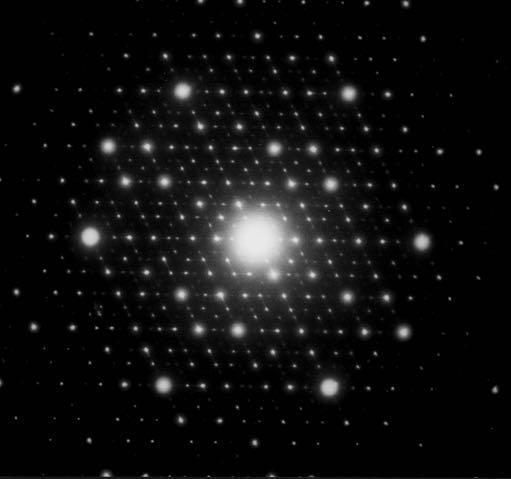

27 MicrodiffracKonpaWernsofsomestatesofmaWer amorphous polycrystalline singlecrystal+disorder cylindrical lauce Quasicrystal seenalonga 23foldaxis B.Devouard
28 Towardveryhigh3resoluKonTEM(HRTEM) Introducing Atomicstructureimages
29 TheobjecKvelensistheonlyonethatmaWers In its focal plane, the diffraction pattern of the object!! In its image plane, the microscope performs!!a Fourier photosummation! A biperiodic image = discrete sum (troncated) of sine variations of fringe contrast along diffraction vectors The Graal: the charge density projection! of the crystal structure!! In the trigonometric form:!! ρ(y,z)= k l F 0kl cos 2π (ky + lz +α 0kl )!! = F 000!! + F 010 cos 2π (y +α 010 ) + F 020 cos 2π (2y+α 020 ) +...!! + F 001 cos 2π (z+α 001 ) + F 002 cos 2π (2z+α 002 ) +...!! + F 011 cos 2π (y+z+α 011 ) + F 022 cos 2π (2y+2z+α 022 ) +...! Amplitude Wavelength Phase

30 Point-to-point resolutions at CINaM: 2.8 Å for 200 kv TEM 1.6Å or 2.1Å for 300kV TEM 0.5Å somewhere in the world Electronic image = recombination of discrete diffracted beams that keep amplitudes and phases of diffracted waves not a «shadow» image but: dynamical diffraction + phase offsets due mainly to spherical aberration The Scherzer defocus (critical underfocusing) roughly compensate for those phase offsets within the transfer window toward the structure image d r = 0, 65λ 3 / 4 Cs 1/ 4 sin χ Fenêtre résolution R0 0,1 0,2 0,3 0, ,3 diaphragme de contraste R (Å -1 ) d (Å)

31 Outoffocus Scherzerdefocus Samethickness


32 CorrectphasesareessenKeltogetacorrectstructureimage ObjecKve Aperture Backfocal plane DiffracKon vectors Wave shir


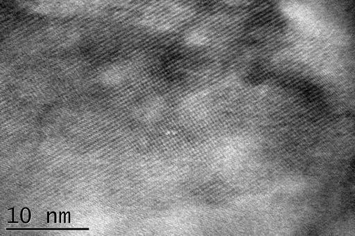
33 VeryHRnumericalscan oftheimage«nuclear»film circularseleckon FFTprocessing (FIJIapplicaKon) l* 04l* 02l* 00l* 5nm Recorded DiffpaWern Quasi3atomicimageof thebioktemicaseen along<100> FFTnowrealisKc subsktutetothe microdiffrackon


34 Summingupprogressively TheFourierterms Lauceimage Thehigh3resoluKonTEM Imageofa2M1phengite 00l* 02l* 04l* Fromlauceimages to structureimages Quasistructureimage

35

36


37 Towardthe3DviewwithaTEM SeeTimm*Weitkamp* wednesdayevening Stereoimaging Electrontomography (JérémieB.tomorrow) SeeJérémie*Berthonneau* tomorrow
ELECTRON MICROSCOPY FOR MULTI-SCALE POROUS MATERIALS PART II - TEM PRINCIPLES
 ELECTRON MICROSCOPY FOR MULTI-SCALE POROUS MATERIALS PART II - TEM PRINCIPLES Marseille Winter School on Multi-Scale Porous Materials (Jan 16-22 2014) A. BARONNET Principles of Transmission Electron Microscopy
Transmission Electron Microscopy (TEM) Prof.Dr.Figen KAYA
 Prof.Dr.Figen KAYA") Transmission Electron Microscopy (TEM) Prof.Dr.Figen KAYA Transmission Electron Microscope A transmission electron microscope, similar to a transmission light microscope, has the following components along
Transmission Electron Microscopy (TEM) Prof.Dr.Figen KAYA Transmission Electron Microscope A transmission electron microscope, similar to a transmission light microscope, has the following components along
11.3 The analysis of electron diffraction patterns
 11.3 The analysis of electron diffraction patterns 277 diameter) Ewald reflecting sphere, the extension of the reciprocal lattice nodes and the slight buckling of the thin foil specimens all of which serve
Electron microscopy II
 Electron microscopy II Nanomaterials characterization I RNDr. Věra Vodičková, PhD. Interaction ction: electrons solid matter Signal types SE.secondary e - AE Auger s e - BSE back scattered e - X-ray photons,
Diffraction Basics. The qualitative basics:
 The qualitative basics: Diffraction Basics Coherent scattering around atomic scattering centers occurs when x-rays interact with material In materials with a crystalline structure, x-rays scattered in
Specimen Preparation Technique for a Microstructure Analysis Using the Focused Ion Beam Process
 Specimen Preparation Technique for a Microstructure Analysis Using the Focused Ion Beam Process by Kozue Yabusaki * and Hirokazu Sasaki * In recent years the FIB technique has been widely used for specimen
Thin Film Scattering: Epitaxial Layers
 Thin Film Scattering: Epitaxial Layers 6th Annual SSRL Workshop on Synchrotron X-ray Scattering Techniques in Materials and Environmental Sciences: Theory and Application May 29-31, 2012 Thin films. Epitaxial
Kinematical theory of contrast
 Kinematical theory of contrast Image interpretation in the EM the known distribution of the direct and/or diffracted beam on the lower surface of the crystal The image on the screen of an EM = the enlarged
TEM imaging and diffraction examples
 TEM imaging and diffraction examples Duncan Alexander EPFL-CIME 1 Diffraction examples Kikuchi diffraction Epitaxial relationships Polycrystalline samples Amorphous materials Contents Convergent beam electron
High Resolution X-ray Diffraction
 High Resolution X-ray Diffraction Nina Heinig with data from Dr. Zhihao Donovan Chen, Panalytical and slides from Colorado State University Outline Watlab s new tool: Panalytical MRD system Techniques:
Transmission Electron Microscopy. J.G. Wen, C.H. Lei, M. Marshall W. Swiech, J. Mabon, I. Petrov
 Advanced Materials Characterization Workshop Transmission Electron Microscopy J.G. Wen, C.H. Lei, M. Marshall W. Swiech, J. Mabon, I. Petrov Supported by the U.S. Department of Energy under grants DEFG02-07-ER46453
Thin Film Characterizations Using XRD The Cases of VO2 and NbTiN
 Thin Film Characterizations Using XRD The Cases of VO2 and NbTiN A thesis submitted in partial fulfillment of the requirement for the degree of Bachelor of Arts / Science in Physics from The College of
INSTRUMENTAL TECHNIQUES FOR PARTICLE SIZE DETERMINATION
 CHAPTER V INSTRUMENTAL TECHNIQUES FOR PARTICLE SIZE DETERMINATION 5.1 INTRODUCTION Particle size determination is very essential and important while working with nanomaterials. There are a few good experimental
Imaging with Diffraction Contrast
 Imaging with Diffraction Contrast Duncan Alexander EPFL-CIME 1 Introduction When you study crystalline samples TEM image contrast is dominated by diffraction contrast. An objective aperture to select either
Atomic Structure of Ultrathin Gold Nanowires
 Supporting Information For Atomic Structure of Ultrathin Gold Nanowires Yi Yu, 1,2 Fan Cui, 1,2 Jianwei Sun, 1,2 and Peidong Yang* 1,2,3,4 1 Department of Chemistry, University of California, Berkeley,
MODEL 1051 TEM Mill ION MILLING. Ion milling is used on physical science. specimens to reduce thickness to electron
 MODEL 1051 TEM Mill A state-of-the-art ion milling and polishing system offering reliable, high performance specimen preparation. It is compact, precise, and consistently produces high-quality transmission
7-2E. Photonic crystals
 7-2E. Photonic crystals Purdue Univ, Prof. Shalaev, http://cobweb.ecn.purdue.edu/~shalaev/ Univ Central Florida, CREOL, Prof Kik, http://sharepoint.optics.ucf.edu/kik/ose6938i/handouts/forms/allitems.aspx
Transmission Kikuchi Diffraction in the Scanning Electron Microscope
 Transmission Kikuchi Diffraction in the Scanning Electron Microscope Robert Keller, Roy Geiss, Katherine Rice National Institute of Standards and Technology Nanoscale Reliability Group Boulder, Colorado
Growth Of TiO 2 Films By RF Magnetron Sputtering Studies On The Structural And Optical Properties
 Journal of Multidisciplinary Engineering Science and Technology (JMEST) Growth Of TiO 2 Films By RF Magnetron Sputtering Studies On The Structural And Optical Properties Ahmed K. Abbas 1, Mohammed K. Khalaf
Practical 2P8 Transmission Electron Microscopy
 Practical 2P8 Transmission Electron Microscopy Originators: Dr. N.P. Young and Prof. J. M. Titchmarsh What you should learn from this practical Science This practical ties-in with the lecture course on
High-resolution phase contrast imaging, aberration corrections, and the specifics of nanocrystals
 High-resolution phase contrast imaging, aberration corrections, and the specifics of nanocrystals Pages 450-459, in Methods and applications in crystallographic computing, S.R. Hall and T. Ashida, Proc.
Supplementary Figure S1 Crystal structure of the conducting filaments in sputtered SiO 2
 Supplementary Figure S1 Crystal structure of the conducting filaments in sputtered SiO 2 based devices. (a) TEM image of the conducting filament in a SiO 2 based memory device used for SAED analysis. (b)
TEM Study of the Morphology Of GaN/SiC (0001) Grown at Various Temperatures by MBE
 Grown at Various Temperatures by MBE") TEM Study of the Morphology Of GaN/SiC (0001) Grown at Various Temperatures by MBE W.L. Sarney 1, L. Salamanca-Riba 1, V. Ramachandran 2, R.M Feenstra 2, D.W. Greve 3 1 Dept. of Materials & Nuclear Engineering,
TEM Study of the Morphology Of GaN/SiC (0001) Grown at Various Temperatures by MBE W.L. Sarney 1, L. Salamanca-Riba 1, V. Ramachandran 2, R.M Feenstra 2, D.W. Greve 3 1 Dept. of Materials & Nuclear Engineering,
Diffraction: Powder Method
 Diffraction: Powder Method Diffraction Methods Diffraction can occur whenever Bragg s law λ = d sin θ is satisfied. With monochromatic x-rays and arbitrary setting of a single crystal in a beam generally
JEOL JXA-8200 Superprobe
 JEOL JXA-8200 Superprobe Electron gun Liq N 2 for EDS Electron gun Condenser lens Optical Microscope Optical Microscope EDS WDS SE Liq N 2 EDS BSE Objective lens WDS Sample exchange chamber Stage High
The Significance of Bragg s Law in Electron Diffraction and Microscopy and Bragg s Second Law
 The Significance of Bragg s Law in Electron Diffraction and Microscopy and Bragg s Second Law Colin Humphreys University of Cambridge Bragg Symposium Adelaide 6 December 2012 Bragg s Second Law E. W.
EBSD Basics EBSD. Marco Cantoni 021/ Centre Interdisciplinaire de Microscopie Electronique CIME. Phosphor Screen. Pole piece.
 EBSD Marco Cantoni 021/693.48.16 Centre Interdisciplinaire de Microscopie Electronique CIME EBSD Basics Quantitative, general microstructural characterization in the SEM Orientation measurements, phase
Specimen configuration
 APPLICATIONNOTE Model 1040 NanoMill TEM specimen preparation system Specimen configuration Preparing focused ion beam (FIB) milled specimens for submission to Fischione Instruments. The Model 1040 NanoMill
MODEL PicoMill TEM specimen preparation system. Achieve ultimate specimen quality free from amorphous and implanted layers
 MODEL 1080 PicoMill TEM specimen preparation system Combines an ultra-low energy, inert gas ion source, and a scanning electron column with multiple detectors to yield optimal TEM specimens. POST-FIB PROCESSING
Experiment 2b X-Ray Diffraction* Optical Diffraction Experiments
 * Experiment 2b X-Ray Diffraction* Adapted from Teaching General Chemistry: A Materials Science Companion by A. B. Ellis et al.: ACS, Washington, DC (1993). Introduction Inorganic chemists, physicists,
Measurement of Residual Stress by X-ray Diffraction
 Measurement of Residual Stress by X-ray Diffraction C-563 Overview Definitions Origin Methods of determination of residual stresses Method of X-ray diffraction (details) References End Stress and Strain
CRYSTAL STRUCTURE DETERMINATION OF PHARMACEUTICALS WITH ELECTRON DIFFRACTION
 CRYSTAL STRUCTURE DETERMINATION OF PHARMACEUTICALS WITH ELECTRON DIFFRACTION Dr. Partha Pratim Das Application Specialist, NanoMEGAS SPRL, Belgium pharma@nanomegas.com www.nanomegas.com This document was
X-Ray Diffraction Analysis
 162402 Instrumental Methods of Analysis Unit III X-Ray Diffraction Analysis Dr. M. Subramanian Associate Professor Department of Chemical Engineering Sri Sivasubramaniya Nadar College of Engineering Kalavakkam
What if your diffractometer aligned itself?
 Ultima IV Perhaps the greatest challenge facing X-ray diffractometer users today is how to minimize time and effort spent on reconfiguring of the system for different applications. Wade Adams, Ph.D., Director,
Sketch the light paths from object to image in a single lens system in following situations.
 Solutions o Chapter I 1.1. There are three rules governing light path or a simple lens: 1) light ray passing through the center o a lens is not deviated. ) Light ray parallel with optic axis will pass
Steps in solving a structure. Diffraction experiment. Obtaining well-diffracting crystals. Three dimensional crystals
 Protein structure from X-ray diffraction Diffraction images: ciprocal space Protein, chemical structure: IALEFGPSLKMNE Conformation, 3D-structure: CRYST1 221.200 73.600 80.900 90.00 90.00 90.00 P 21 21
X-RAY POWDER DIFFRACTION XRD
 X-RAY POWDER DIFFRACTION XRD for the analyst Getting acquainted with the principles Martin Ermrich nλ = 2d sin θ Detlef Opper The Analytical X-ray Company X-RAY POWDER DIFFRACTION XRD for the analyst Getting
Principles & Practice of Electron Diffraction
 Principles & Practice of Electron Diffraction Duncan Alexander EPFL-CIME 1 Contents Introduction to electron diffraction Elastic scattering theory Basic crystallography & symmetry Electron diffraction
MODEL TEM Mill. Two independently adjustable TrueFocus ion sources
 MODEL 1050 TEM Mill A state-of-the-art ion milling and polishing system. It is compact, precise, and consistently produces high-quality transmission electron microscopy (TEM) specimens with large electron
EBSD Electron BackScatter Diffraction Principle and Applications
 EBSD Electron BackScatter Diffraction Principle and Applications Dr. Emmanuelle Boehm-Courjault EPFL STI IMX Laboratoire de Simulation des Matériaux LSMX emmanuelle.boehm@epfl.ch 1 Outline! Introduction!
Microstructural parameters from Multiple Whole Profile (MWP) or Convolutional Multiple Whole Profile (CMWP) computer programs
 or Convolutional Multiple Whole Profile (CMWP) computer programs") Microstructural parameters from Multiple Whole Profile (MWP) or Convolutional Multiple Whole Profile (CMWP) computer programs Iuliana Dragomir-Cernatescu School of Materials Science and Engineering, Georgia
Microstructural parameters from Multiple Whole Profile (MWP) or Convolutional Multiple Whole Profile (CMWP) computer programs Iuliana Dragomir-Cernatescu School of Materials Science and Engineering, Georgia
Focused Ion Beam CENTRE INTERDISCIPLINAIRE DE MICROSCOPIE ELECTRONIQUE. Marco Cantoni, EPFL-CIME CIME ASSEMBLEE GENERALE 2007
 Focused Ion Beam @ CENTRE INTERDISCIPLINAIRE DE MICROSCOPIE ELECTRONIQUE Present situation and vision Marco Cantoni, EPFL-CIME Dual Beam Nova 600 Nanolab from FEI Company FE-SEM & FIB: Ga LMIS 4 Gas Injector
Travaux Pratiques de Matériaux de Construction. Etude de Matériaux Cimentaires par Diffraction des Rayons X sur Poudre
 Travaux Pratiques de Matériaux de Construction Section Matériaux 6 ème semestre 2015 Etude de Matériaux Cimentaires par Diffraction des Rayons X sur Poudre Study Cementitious Materials by X-ray diffraction
Transparent Ceramic Yb 3+ :Lu2O3 Materials
 Contract no.: FA2386-10-1-4113 Final report for the project on: Transparent Ceramic Yb 3+ :Lu2O3 Materials Submission Date: Jan 19 th, 2012 Principal Investigator: Dr. Akio Ikesue World-Lab. Co., Ltd.
X ray diffraction in materials science
 X ray diffraction in materials science Goals: Use XRD spectra to determine the orientation of single crystals and preferred orientations in a thin film. Understand how grain size and strain affect the
Combinatorial RF Magnetron Sputtering for Rapid Materials Discovery: Methodology and Applications
 Combinatorial RF Magnetron Sputtering for Rapid Materials Discovery: Methodology and Applications Philip D. Rack,, Jason D. Fowlkes, and Yuepeng Deng Department of Materials Science and Engineering University
AP 5301/8301 Instrumental Methods of Analysis and Laboratory Lecture 5 X ray diffraction
 1 AP 5301/8301 Instrumental Methods of Analysis and Laboratory Lecture 5 X ray diffraction Prof YU Kin Man E-mail: kinmanyu@cityu.edu.hk Tel: 3442-7813 Office: P6422 Lecture 5: Outline Review on crystallography
Earth & Planetary Science Applications of X-Ray Diffraction: Advances Available for Research with our New Systems
 Earth & Planetary Science Applications of X-Ray Diffraction: Advances Available for Research with our New Systems James R. Connolly Dept. of Earth & Planetary Sciences University of New Mexico 401/501
3D-EBSD an CrossBeam-Systemen
 FIB- Workshop 3.-4. July 2008 3D-EBSD an CrossBeam-Systemen Ulrike Zeile 1, Ali Gholinia 2 and Frank Bauer 3 Arbeitskreis FIB SSOM DGM/DGE ASEM Hotel Seeburg, Luzern, Switzerland 1. Carl Zeiss NTS 2. Oxford
Materials Characterization for Stress Management
 Materials Characterization for Stress Management Ehrenfried Zschech, Fraunhofer IZFP Dresden, Germany Workshop on Stress Management for 3D ICs using TSVs San Francisco/CA, July 13, 2010 Outline Stress
Structure Analysis of -phase in Sb-Te Alloys by HRTEM* 1
 Materials Transactions, Vol. 45, No. 8 (2004) pp. 2673 to 2677 #2004 The Japan Institute of Metals Structure Analysis of -phase in Sb-Te Alloys by HRTEM* 1 Yoshiyuki Nakata 1, Takehito Suenaga 1; * 2,
DIFFRACTION METHODS IN MATERIAL SCIENCE. PD Dr. Nikolay Zotov Tel Room 3N16.
 DIFFRACTION METHODS IN MATERIAL SCIENCE PD Dr. Nikolay Zotov Tel. 0711 689 3325 Email: zotov@imw.uni-stuttgart.de Room 3N16 Lecture 7 OUTLINE OF THE COURSE 0. Introduction 1. Classification of Materials
Basic Crystallography
 Basic Crystallography Data collection and processing Louise N. Dawe, PhD Wilfrid Laurier University Department of Chemistry and Biochemistry References and Additional Resources Faculty of Science, Bijvoet
X-ray diffraction and structure analysis Introduction
 Teknillisen fysiikan ohjelmatyö X-ray diffraction and structure analysis Introduction Oleg Heczko 120 100 80 118 12-5 125 Ni-Mn-Ga (298K) SQRT(Intensity) 60 40 20 015 200 123 12-7 20-10 20,10 20-8 040
Lawrence Berkeley National Laboratory Lawrence Berkeley National Laboratory
 Lawrence Berkeley National Laboratory Lawrence Berkeley National Laboratory Title Lorentz transmission electron microscopy investigation of magnetically patterned Co/Pt multilayers Permalink https://escholarship.org/uc/item/6gr7d3t3
Repetition: Adhesion Mechanisms
 Repetition: Adhesion Mechanisms a) Mechanical interlocking b) Monolayer/monolayer c) Chemical bonding d) Diffusion e) Psedo diffusion due to augmented energy input (hyperthermal particles) Repetition:
Travaux Pratiques de Matériaux de Construction
 Travaux Pratiques de Matériaux de Construction Section Matériaux 6 ème semestre 2009 Etude de Matériaux Cimentaire Par Diffraction des Rayons X Responsable: Silke Ruffing E-Mail: silke.ruffing@epfl.ch
UNIT V -CRYSTAL STRUCTURE
 UNIT V -CRYSTAL STRUCTURE Solids are of two types: Amorphous and crystalline. In amorphous solids, there is no order in the arrangement of their constituent atoms (molecules). Hence no definite structure
Structural and Optical Properties of Aluminium Antimonide Thin Films Deposited By Thermal Evaporation Method
 Available online at www.scholarsresearchlibrary.com Scholars Research Library Archives of Physics Research, 2011, 2 (1): 146-153 (http://scholarsresearchlibrary.com/archive.html) ISSN 0976-0970 CODEN (USA):
DIFFRACTION METHODS IN MATERIAL SCIENCE. Lecture 7
 DIFFRACTION METHODS IN MATERIAL SCIENCE PD Dr. Nikolay Zotov Tel. 0711 689 3325 Email: zotov@imw.uni-stuttgart.de Room 3N16 Lecture 7 Practicum 15.12.2016 15:15 Room 3P2! Lectures 16.12.2016 11:00 Room
Instrument Configuration for Powder Diffraction
 Instrument Configuration for Powder Diffraction Advanced X-ray Workshop S.N. Bose National Centre for Basic Sciences, 14-15/12/2011 Innovation with Integrity Overview What is the application? What are
Department of Mechanical Engineering, University of Michigan, Ann Arbor, Michigan 48109, United States
 Eric Kazyak a, Kuan-Hung Chen a, Kevin N. Wood a, Andrew L. Davis a, Travis Thompson a, Ashley R. Bielinski a, Adrian Sanchez a, Xiang Wang b, Chongmin Wang c, Jeff Sakamoto a, Neil P. Dasgupta a a Department
Structural and optical characterization of reactive evaporated tin diselenide thin films
 IOP Conference Series: Materials Science and Engineering OPEN ACCESS Structural and optical characterization of reactive evaporated tin diselenide thin films Recent citations - Studies on Physical Properties
What is a positron moderator?
 What is a positron moderator? The advent of slow positron beams has resulted in nondestructive depth profiling of defects in surfaces and interfaces, low energy positron diffraction and positron remission
Electron Beam Induced Processes and their Applicability to Mask Repair
 & Electron Beam Induced Processes and their Applicability to Mask Repair Hans W.P. Koops (1), Volker Boegli (1), Klaus Edinger (1), Johannes Bihr (2), Jens Greiser (2), (1) NaWoTec GmbH Rossdorf Germany
LORENTZ TRANSMISSION ELECTRON MICROSCOPY INVESTIGATION OF MAGNETICALLY PATTERNED Co/Pt MULTILAYERS
 LORENTZ TRANSMISSION ELECTRON MICROSCOPY INVESTIGATION OF MAGNETICALLY PATTERNED Co/Pt MULTILAYERS G.J. KUSINSKI 1,2, K.M. KRISHNAN 2, D. WELLER 3, B.D. TERRIS 3, L. FOLKS 3, A.J. KELLOCK 3, J.E.E. BAGLIN
Aberration corrected high-resolution transmission and scanning transmission electron microscopy of thin perovskite layers
 Available online at www.sciencedirect.com Physics Procedia 40 (2013 ) 49 55 2 nd European Conference on Nano Films: ECNF-2012 Aberration corrected high-resolution transmission and scanning transmission
Rietveld refinement of ZrSiO 4 : application of a phenomenological model of anisotropic peak width
 Rietveld refinement of ZrSiO 4 : application of a phenomenological model of anisotropic peak width A. Sarkar, P. Mukherjee, P. Barat Variable Energy Cyclotron Centre 1/A Bidhan Nagar, Kolkata 700064, India
Relation Between Internal Stress and Surface Roughness of Titanium Nitride Films Deposited by HCD Ion Plating
 No.22,28 65 Relation Between Internal Stress and Surface Roughness of Titanium Nitride Films Deposited by HCD Ion Plating Itsuo Ishigami Ken-ichi Miura Hideaki Hoshino Tomoyuki Mizukoshi (28 6 17 ) An
Basic X-ray Powder Diffraction (XRPD)
") Basic X-ray Powder Diffraction (XRPD) Solid-State, Material Science Crystalline (Scattering : diffraction) Non-crystalline (Scattering) Analytical Tool Qualitative and Quantitative Analysis Quantitative
Basic X-ray Powder Diffraction (XRPD) Solid-State, Material Science Crystalline (Scattering : diffraction) Non-crystalline (Scattering) Analytical Tool Qualitative and Quantitative Analysis Quantitative
A Brief History of XRD 1895: Röntgen discovers X-Rays received the first Nobel prize in physics in 1901
 X-ray Diffraction A Brief History of XRD 1895: Röntgen discovers X-Rays received the first Nobel prize in physics in 1901 1912: Laue diffracts X-Rays from single crystal 1914 Nobel prize in Physics 1912:
X-ray Powder Diffraction in Catalysis
 X-ray Powder Diffraction in Catalysis 0/63 Introduction Introduction: scope of this lecture This lecture is designed as a practically oriented guide to powder XRD in catalysis, not as an introduction into
Supporting Information. Low temperature synthesis of silicon carbide nanomaterials using
 Supporting Information Low temperature synthesis of silicon carbide nanomaterials using solid-state method Mita Dasog, Larissa F. Smith, Tapas K. Purkait and Jonathan G. C. Veinot * Department of Chemistry,
Supporting Information
 Supporting Information Experimental Methods Pt ALD. The precursor used for ALD was trimethyl-methylcyclopentadienyl-platinum(iv) (MeCpPtMe 3 ) (Strem Chemicals, 99%), which has been widely reported for
Solar Cells and Photosensors.
 Designing Photonic Crystals in Strongly Absorbing Material for Applications in Solar Cells and Photosensors. Minda Wagenmaker 1, Ebuka S. Arinze 2, Botong Qiu 2, Susanna M. Thon 2 1 Mechanical Engineering
Metallization deposition and etching. Material mainly taken from Campbell, UCCS
 Metallization deposition and etching Material mainly taken from Campbell, UCCS Application Metallization is back-end processing Metals used are aluminum and copper Mainly involves deposition and etching,
XRD and TEM analysis of microstructure in the welding zone of 9Cr 1Mo V Nb heat-resisting steel
 Bull. Mater. Sci., Vol. 25, No. 3, June 2002, pp. 213 217. Indian Academy of Sciences. XRD and TEM analysis of microstructure in the welding zone of 9Cr 1Mo V Nb heat-resisting steel LI YAJIANG*, WANG
Physical structure of matter. Monochromatization of molybdenum X-rays X-ray Physics. What you need:
 X-ray Physics Physical structure of matter Monochromatization of molybdenum X-rays What you can learn about Bremsstrahlung Characteristic radiation Energy levels Absorption Absorption edges Interference
MODEL SEM Mill. Two independently adjustable TrueFocus ion sources
 MODEL 1060 SEM Mill A state-of-the-art ion milling and polishing system. It is compact, precise, and consistently produces high-quality scanning electron microscopy (SEM) samples for a wide variety of
Annealing Effect on Elastic Constant of Ultrathin Films Studied by Acoustic-Phonon Resonance Spectroscopy
 1st International Symposium on Laser Ultrasonics: Science, Technology and Applications July 16-18 28, Montreal, Canada Annealing Effect on Elastic Constant of Ultrathin Films Studied by Acoustic-Phonon
Characterization of Nano-Scale Fine Precipitates in Al-Mg-Si Alloys for Automotive Applications
 UDC 669. 715 721 782 : 629. 11. 011. 5 Characterization of Nano-Scale Fine Precipitates in Al-Mg-Si Alloys for Automotive Applications Makoto SAGA* 1 Naoki MARUYAMA* 1 Abstract Bake-hadenable Al-Mg-Si
Quiz on Monday covering: -symmetry operations -notations of axes, vectors, and face notation -Miller indices
 OTHER ANNOUNCEMENTS Quiz on Monday covering: -symmetry operations -notations of axes, vectors, and face notation -Miller indices 2 nd Draft of References due Monday Field Trip Saturday 10/4 and Sunday
Development of photonic and thermodynamic crystals conforming to sustainability conscious materials tectonics
 Sustainable Chemistry 103 Development of photonic and thermodynamic crystals conforming to sustainability conscious materials tectonics S. Kirihara, N. Ohta, T. Niki, Y. Uehara & S. Tasaki Joining and
SPECIMEN PREPARATION FOR ELECTRON MICROSCOPY
 SPECIMEN PREPARATION FOR ELECTRON MICROSCOPY Samar Das Scientist National Metallurgical Laboratory Jamshedpur - 831 007 The purpose of electron microscopy is to study accurately the microstructures at
The growth of patterned ceramic thin films from polymer precursor solutions Göbel, Ole
 University of Groningen The growth of patterned ceramic thin films from polymer precursor solutions Göbel, Ole IMPORTANT NOTE: You are advised to consult the publisher's version (publisher's PDF) if you
Electron Microscopy Sciences Industry Road. P.O. Box 550. Hatfield, PA Introduction. DuraSiNTM
 DuraSiNTM Electron Microscopy Sciences Introduction DuraSiN TM Film and Mesh products have revolutionized the way samples are prepared for and analyzed in the transmission electron microscope. DuraSiN
Review key concepts from last lecture (lattice + basis = unit cell) Bravais lattices Important crystal structures Intro to miller indices
 Bravais lattices Important crystal structures Intro to miller indices") Outline: Review key concepts from last lecture (lattice + basis = unit cell) Bravais lattices Important crystal structures Intro to miller indices Review (example with square lattice) Lattice: square,
Outline: Review key concepts from last lecture (lattice + basis = unit cell) Bravais lattices Important crystal structures Intro to miller indices Review (example with square lattice) Lattice: square,
Condensed Matter II: Particle Size Broadening
 Condensed Matter II: Particle Size Broadening Benjamen P. Reed & Liam S. Howard IMAPS, Aberystwyth University March 19, 2014 Abstract Particles of 355µm silicon oxide(quartz)were subjected to a ball milling
The changes of ADI structure during high temperature annealing
 ARCHIVES of FOUNDRY ENGINEERING Published quarterly as the organ of the Foundry Commission of the Polish Academy of Sciences ISSN (1897-3310) Volume 10 Issue Special1/2010 87-92 15/1 The changes of ADI
GEOLOGY 333 LAB 14. Lab Final Exam See information sheet for details
 GEOLOGY 333 LAB 14 X-RAY DIFFRACTION OF EVERYDAY MATERIALS Lab Final Exam See information sheet for details! Next week during Lab (10 am - noon, May 2, 69 CAB).! 25% of Lab grade, out of 65 points plus
Solving Problems in Surface Engineering and Tribology by Means of Analytical Electron Microscopy
 Digital Comprehensive Summaries of Uppsala Dissertations from the Faculty of Science and Technology 12 Solving Problems in Surface Engineering and Tribology by Means of Analytical Electron Microscopy ERNESTO
LOT. Contents. Introduction to Thin Film Technology. Chair of Surface and Materials Technology
 Introduction to Thin Film Contents 1. Introduction and Application Examples (2h) 2. Preparation of Thin Films by PVD (Physical Vapor Deposition) (6h) 2.1 Vacuum Technique (1h) 2.1.1 Kinetics of Gases 2.1.2
Precision Optical Engineering
 Precision Optical Engineering Products: Prisms Windows Mirrors Flats and Master angles Sight Glasses Key Features: Prisms (Contacted, Cemented, AR coated, Mounted) Windows (Flat, wedged, curved, drilled,
Thin Films & AR Coated. Viewports. Thin Film & AR Coated. Viewports
 Thin Films & AR Item Page Thin Film Coatings Introduction P 02 Kodial Zero Length with Anti-Reflective Coatings P 04 Kodial Zero Length with Anti-Reflective Coatings-Non-Magnetic P 07 Kodial Zero Length
YHITE BEAM SYNCHROTRON X-RAY TOPOGRAPHY OF GALLIUM ARSENIDE
 YHITE BEAM SYNCHROTRON X-RAY TOPOGRAPHY OF GALLIUM ARSENIDE John M. Yinter, Jr., and Robert E. Green, Jr. Center for Nondestructive Evaluation The Johns Hopkins University Baltimore, Maryland, 21218 Yilliam
Small-angle X-ray scattering (SAXS) with synchrotron radiation
 with synchrotron radiation") Small-angle X-ray scattering (SAXS) with synchrotron radiation Martin Müller Institut für Experimentelle und Angewandte Physik der Christian-Albrechts-Universität zu Kiel Introduction to small-angle scattering
Small-angle X-ray scattering (SAXS) with synchrotron radiation Martin Müller Institut für Experimentelle und Angewandte Physik der Christian-Albrechts-Universität zu Kiel Introduction to small-angle scattering
Thin Films: Sputtering Systems (Jaeger Ch 6 & Ruska Ch 7,) Can deposit any material on any substrate (in principal) Start with pumping down to high
 Can deposit any material on any substrate (in principal) Start with pumping down to high") Thin Films: Sputtering Systems (Jaeger Ch 6 & Ruska Ch 7,) Can deposit any material on any substrate (in principal) Start with pumping down to high vacuum ~10-7 torr Removes residual gases eg oxygen from
Thin Films: Sputtering Systems (Jaeger Ch 6 & Ruska Ch 7,) Can deposit any material on any substrate (in principal) Start with pumping down to high vacuum ~10-7 torr Removes residual gases eg oxygen from
Introduction to Electron Backscattered Diffraction. TEQIP Workshop HREXRD Feb 1 st to Feb 5 th 2016
 Introduction to Electron Backscattered Diffraction 1 TEQIP Workshop HREXRD Feb 1 st to Feb 5 th 2016 SE vs BSE 2 Ranges and interaction volumes 3 (1-2 m) http://www4.nau.edu/microanalysis/microprobe/interact-effects.html
JECP/HOLZ, an Interactive Computer Program for Simulation of HOLZ Pattern
 JECP/HOLZ, an Interactive Computer Program for Simulation of HOLZ Pattern (Version 2t) X.Z. Li, Ph. D Copyright(C) 2002-2017 LANDYNE All Rights Reserved. Contents: 1. Purpose of the program 2. Graphic
EFFECT OF DEPOSITION TIME ON CHEMICAL BATH DEPOSITION PROCESS AND THICKNESS OF BaSe THIN FILMS.
 Journal of Optoelectronics and Biomedical Materials Vol. 3 Issue 4, October-December 2011 p. 81-85 EFFECT OF DEPOSITION TIME ON CHEMICAL BATH DEPOSITION PROCESS AND THICKNESS OF BaSe THIN FILMS. N.A. OKEREKE