Verfahrens- und Systemtechnik zum präzisen Hochleistungsabtrag mit UKP-Lasern
|
|
|
- Maurice Charles
- 5 years ago
- Views:
Transcription

1 Verfahrens- und Systemtechnik zum präzisen Hochleistungsabtrag mit UKP-Lasern Jens Holtkamp
")
 at the University of")
2 Motivation Ultra short pulsed lasers National Institute of Standards and Technology (NIST) Regional Laser and Biomedical Technology Laboratories (RLBL) at the University of Pennsylvania


3 Motivation High Power Ultra-short pulse laser sources
4 Number of Lasers per Year Motivation Number of ultrashort-pulsed Lasers for Material Processing Estimated market growth for the next years: ca. 30 % Year market estimation by Fraunhofer ILT

5 Motivation Potential of ultrashort-pulsed Lasers Substitution of existing Technologies e.g. Etching, Erosion, Cutting Development of new Technologies e.g. Thin film ablation, Surface functionalisation Advantages of ultrashort-pulsed Lasers (quasi) Material independant (quasi) no thermal influence Tool-free, wear-free and resource-efficient Almost no lead-time (Digital Photonic Production) Highest precision (lateral and vertical) Universal application (due to high variety of parameters)


6 Motivation Areas of Application
 Light guidance Wafer Dicing")
7 Motivation Megatrends Areas of Application Display / Light (Thin-)Glass cutting Thin film ablation Mask production for coating technologies Energy Photovoltaik: Texturing, Drilling, Doping Wind: Surface structuring of rotor blades Lightweight construction Cutting and Repair of Fiber reinforced plastics Resource efficiency Functional surfaces (Wetting, Tribology) Light guidance Wafer Dicing Environment Filter for Water treatment


8 Basics Tailored Light at Fraunhofer ILT Simulation Interaction of laser radiation with material Simulation of ablation processes Development of ablation tools System Technology New high power ps and fs Laser Special Optics Machine Technology Deflection Systems Process monitoring Process development Use of different kind of laser systems and optics Development of ablation strategies Small batch production and Industrial validation


9 Basics Process concept for laser micro ablation Structuring of any geometries 3D without noticable steps in thin layers Typical parameters Focus diameter: 5-20 µm Line distance: 5-10 µm Layer thickness: 0,1-1 µm Randschnitte Schraffur Brennfleck Spurabstand Bearbeitungsspuren Schnitt mit Bearbeitungsschichten
10 Basics Process concept for laser micro ablation Average Power: up to 1 kw (Fa. Amphos) Repetition Rate: khz MHz (typ. 500 khz) Pulse Energy: µj mj (typ. < 10 µj) Pulse Power: 100 MW Intensity: 100 TW/cm 2 = W/cm (10 µm) 2 Ablation Rate: up to 20 mm 3 /min (typ. < 5 mm 3 /min) Wavelength 266 nm nm
 Ablation mainly by vapourisation Minimal thermal")
11 Basics Ultra short laser pulse interaction with metals Time Ranges of Energy Transfer Photon Electron: <10 fs Electron Electron: <100 fs Electron Lattice: 1-10 ps Lattice Lattice: speed of sound No interaction of radiation with vapour and melt (Heating after end of laser pulse) Ablation mainly by vapourisation Minimal thermal influence
12 Basics Ultra short laser pulse interaction with metals Laser Melt T v Vapor Melt dominated T m T m Melt Heating Vaporization Expulsion Result Laser Vapor T v Vapor dominated T m Melt T m T v d DR 2r DR


13 Basics Multipass-Ablation of Composite Materials tpulse = 100 ns Rep.-rate: 100 khz Pulse energy: 50µJ VScan: 1m/s Layer Thickness: 20 µm tpulse = 10ps Rep.-rate: 100 khz Pulse Energy: 30µJ VScan: 1m/s Layer Thickness: 10 µm
short")


14 Basics Laser Ablation with (Ultra-)short pulse Laser Time for manufacturing 10 hours Ablated volume 100 mm 3 Quality of ablation comparable to EDM No tools needed ns-laser ps-laser Eroded


15 Functional Surfaces Micro injection moulding of lens arrays with ps-laser Surface quality After Laser ablation: R a = 300nm After Laser polishing: R a = 100nm


16 Functional Surfaces Laser Structuring of Motor Components Aim: reduction of friction and wear Structures act as oil reservoir and a hydrodynamic bearing Compromise between efficiency and oil comsumption


17 Functional Surfaces Laser Structuring of Motor Components Inserting of micro structures by ps laser ablation No further treatment necessary No thermal degradation of the adjoined material Applications in automotive industry under development Piston rings Cylinders Sealing rings Piston pumps Laser structured piston rings

18 Functional Surfaces Surface roughening Nanoripples Cone-like-protrusions (CLPs) Statistical structure effect that occurs by redistribution of melt during ablation with ultrashort laser pulses Structure sizes: 6-10µm Nano ripples Overlay of nanostructures Structure size: ~1µm


")

19 Functional Surfaces Surface roughening ablation of layers with high laser intensity generation of structures with high aspect ratio (>10) Applications anti-reflection surface scattering area Change of wetting behaviour
 Contact angle > 150 Hydrophylic coating CLP (6-7µm) HMDSO Plasma Coating with oxygen")
20 Functional Surfaces CLPs - Extreme enhancement of the surface area Hydrophobic coating CLP (6-7µm) HMDSO Plasma Coating (300nm) Contact angle > 150 Hydrophylic coating CLP (6-7µm) HMDSO Plasma Coating with oxygen (300nm)
 No damage of the substrate No")
 Applications OLED Lighting and Display Thin film PV PEDOT:PSS 248nm s= 1.6 ± 0.")
21 Functional Surfaces Thin film processing Requirements for large area electronics: Fast, High resolution Shape independent Different kind of layer materials and thicknesses (organic and anorganic) No damage of the substrate No delamination Used Laser Excimer (193 nm, 248 nm, ns, mask projection) Ultrafast laser (355, 532, 1064, fs ps, Scanner deflection) Applications OLED Lighting and Display Thin film PV PEDOT:PSS 248nm s= 1.6 ± 0.2 µm SnO on glass 10 ps, 355nm


22 700 µm Cutting Thin glass processing Cutting by ablation Pulse duration 10 ps Wavelength 532 nm Average Power 20 W Number of layers 100 Scan speed 2 4 m/s front side 300 µm


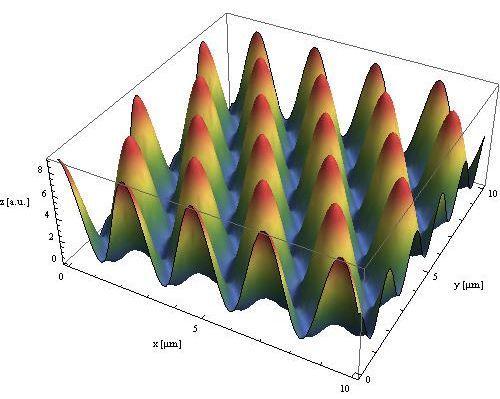
23 Periodic Nano Structuring Interference Technique
![Periode [µm] Periodic Nano Structuring Interference Technique](/docs-images/80/81766147/images/24-0.jpg "Periodicity controlled by: Laser wavelength Beam configuration")

24 Periode [µm] Periodic Nano Structuring Interference Technique Periodicity controlled by: Laser wavelength Beam configuration Intersection angle µm µm µm µm Formula: 1 Factor depends on beam configuration Winkel [Grad]


25 Periodic Nano Structuring Interference Technique Potential Structures sizes: 100 nm nm High uniformity of the created structures Whole beam diameter is structured simultaneously Non-flat surfaces can be processed Nearly material independent Only one process step Challenges Gaussian beam profile leads to variations in structure size and depth over a spot Stitching necessary to structure area larger than the spot diameter Laboratory stage


26 Periodic Nano Structuring Multi-Beam-Interference Structure geometry: Ø1 µm; depth: 600 nm Material: PEEK holes with one shot Homogeneous structures over the entire spot (Ø500 µm) 5µm
27 Periodic Nano Structuring Multi-Beam-Interference Material: Stainless Steel Periodicity: 530 nm Focal diameter: 60 µm Wavelength: 355 nm 10 ps pulse duration 1 cm


28 Periodic Nano Structuring Multi-Beam-Interference Structure geometry: Ø1,6 µm; Depth: 2,3 µm Material: Quartz glass Structuring into Photoresist Subsequent Reactiv Ion Etching


29 Periodic Nano Structuring Interference Technique Parameter Laser: 355nm, 400kHz, 10 ps Material: Brass Spot size: µm Feed rate: 4500 mm/min Periodicty: 780 nm line structure hole structure Spot by spot pulse overlap


30 Future Developments High Precision at Large Components Cutting of fiber reinforced polymers Large area processing Surface structuring Low friction surfaces
31 Large area processing System strategies high pulse energy / low reprate? t t or high reprate / low pulse energy?
 Focal distance: 163 mm Focal diameter: 20-25 µm Scan-field: 100x100 mm 2 Data import: Bitmap, PNG, 2D Array (Gray-scale value corresponds to number of Layers)")
32 Large area processing Polygonic Mirror Max. Scan velocity: 340 m/s (max. rpm: ) Focal distance: 163 mm Focal diameter: µm Scan-field: 100x100 mm 2 Data import: Bitmap, PNG, 2D Array (Gray-scale value corresponds to number of Layers) Additional linear motor Number of mirrors: 11 Max. Output Frequency: modulated 20 MHz; digital 40 MHz
 10 MHz Output Frequency Feed rate: 18 mm/s 2800")
33 Large area processing Polygonic Mirror Chess pattern Calculation on FPGA 40 MHz Output Frequency Feed rate: 35 mm/s 9500 rpm AC Dom, ILT + Polyscan Logo PNG-Import (25 MPix) 10 MHz Output Frequency Feed rate: 18 mm/s 2800 rpm


34 Large area processing Multi-beam laser processing with DOEs Laser source DOE 2x2 mask Periodic structures Split high pulse energy into numerous partial beams
35 Large area processing Micro structured Embossing rolls Material: chrome-plated Copper Dimensions: Ø250 mm; length 1 m Rotational speed: 1400 rpm (v= 15 m/s) Line distance: 2 µm Focus diameter: 10 µm Laser power: 100 W 5 mm Surface roughness <0,5 µm Min. structure size: 5 µm No burr
36 Large area processing Micro structured Embossing rolls Higher ablation rate by additional scanning device Pulse overlap is controlled by rotational speed (fixed rep.rate) 3 mm min 20 Movement of Laser 10 MHz 90 m/s Surface speed Pulse overlap (@ 2 MHz) 1m/s 90% 10m/s 20m/s 50% 0% Movement of workpiece 5 2 MHz, 18 m/s, PO 25% 5 40 Cylinder surface speed m s

37 Future Developments Ultrafast Manufacturing Today: Typical ablation rates of e.g. Aluminum ca. 1 mm 3 /min Limited by max. Laser power and Scanning speed Future potential: Ablation rates of >5 mm 3 /sec Use of fast deflection systems and >1 kw average Power Direct manufacturing of small components e.g. with specific surface features

38 SAVE THE DATE
Micro processing with laser radiation
 Micro processing with laser radiation Trends and perspectives Miniaturization and highly integrated functionalization are the driving factors in the production of innovative products in almost every industrial
Laser Micromachining of Bulk Substrates and Thin Films Celine Bansal
 Laser Micromachining of Bulk Substrates and Thin Films Celine Bansal Oxford Lasers Ltd Moorbrook Park Didcot, Oxfordshire, OX11 7HP Tel: +44 (0) 1235 810088 www.oxfordlasers.com Outline Oxford Lasers Importance
11.3 Polishing with Laser Radiation
 196 E. Willenborg 11.3 Polishing with Laser Radiation Edgar Willenborg The surface roughness of a part or product strongly influences its properties and functions. Among these can be counted abrasion and
Rapid Microtooling with laser based methods
 Hochschule Mittweida University of Applied Sciences Rapid Microtooling with laser based methods R. Ebert, U. Löschner, A. Streek, J. Schille, T. Süß, L. Hartwig, U. Klötzer, H. Exner ISL 2008 Chemnitz
Aluminum / Copper oscillation welding with a 500 W direct diode laser
 Application Note Issued: 2016-06-01 Aluminum / Copper oscillation welding with a 500 W direct diode laser SUMMARY The performance of the 500 W DirectProcess direct diode laser for oscillating welding by
Lasers and Laser Systems for Micro-machining
 Lasers and Laser Systems for Micro-machining Martyn Knowles Oxford Lasers Ltd Unit 8, Moorbrook Park Didcot, Oxfordshire, OX11 7HP Tel: +44 (0) 1235 810088 www.oxfordlasers.com Lasers and Laser Systems
Applications of Systems for Beam Shaping in Material Processing Pulsar Photonics GmbH
 LASER World of Photonics 2015 Workshop Using Diffractive Optics Applications of Systems for Beam Shaping in Material Processing Pulsar Photonics GmbH Speaker Dipl. Phys. Stephan Eifel, Pulsar Photonics
Available online at ScienceDirect. Physics Procedia 56 (2014 ) Ultra-short pulse laser structuring of molding tools
 Ultra-short pulse laser structuring of molding tools") Available online at www.sciencedirect.com ScienceDirect Physics Procedia 56 (2014 ) 1041 1046 8 th International Conference on Photonic Technologies LANE 2014 Ultra-short pulse laser structuring of molding
Available online at www.sciencedirect.com ScienceDirect Physics Procedia 56 (2014 ) 1041 1046 8 th International Conference on Photonic Technologies LANE 2014 Ultra-short pulse laser structuring of molding
EFFICIENCY AND PRODUCTIVITY INCREASE OF SOLAR-CELLS AND -MODULES BY INNOVATIVE LASER APPROACHES
 EFFICIENCY AND PRODUCTIVITY INCREASE OF SOLAR-CELLS AND -MODULES BY INNOVATIVE LASER APPROACHES PD Dr. Alexander Horn, V. Schütz, J. Gonzalez, C.C. Kalmbach Photovoltaics Group Dpt. for Production and
Picosecond Laser Patterning of ITO Thin Films
 Available online at www.sciencedirect.com Physics Procedia 12 (2011) 133 140 LiM 2011 Picosecond Laser Patterning of ITO Thin Films Anna Risch*, Ralf Hellmann University of Applied Sciences Aschaffenburg,
Microstructuring of Steel and Hard Metal using Femtosecond Laser Pulses
 Available online at www.sciencedirect.com Physics Procedia 12 (2011) 60 66 LiM 2011 Microstructuring of Steel and Hard Metal using Femtosecond Laser Pulses Manuel Pfeiffer a *, Andy Engel a, Steffen Weißmantel
Chapter 3 Silicon Device Fabrication Technology
 Chapter 3 Silicon Device Fabrication Technology Over 10 15 transistors (or 100,000 for every person in the world) are manufactured every year. VLSI (Very Large Scale Integration) ULSI (Ultra Large Scale
High Throughput Laser Processing of Guide Plates for Vertical Probe Cards Rouzbeh Sarrafi, Dana Sercel, Sean Dennigan, Joshua Stearns, Marco Mendes
 High Throughput Laser Processing of Guide Plates for Vertical Probe Cards Rouzbeh Sarrafi, Dana Sercel, Sean Dennigan, Joshua Stearns, Marco Mendes IPG Photonics - Microsystems Division Outline Introduction
3 Pulsed laser ablation and etching of fused silica
 3 Pulsed laser ablation and etching of fused silica 17 3 Pulsed laser ablation and etching of fused silica Material erosion caused by short laser pulses takes place far from equilibrium and may be based
INFLUENCE OF LASER ABLATION ON STAINLESS STEEL CORROSION BEHAVIOUR
 INFLUENCE OF LASER ABLATION ON STAINLESS STEEL CORROSION BEHAVIOUR Michal ŠVANTNER a, Martin KUČERA b, Šárka HOUDKOVÁ c, Jan ŘÍHA d a University of West Bohemia, Univerzitní 8, 306 14 Plzeň, msvantne@ntc.zcu.cz
MICROFABRICATION OF OPTICALLY ACTIVE InO X MICROSTRUCTURES BY ULTRASHORT LASER PULSES
 Journal of Optoelectronics and Advanced Materials Vol. 4, No. 3, September 2002, p. 809-812 MICROFABRICATION OF OPTICALLY ACTIVE InO X MICROSTRUCTURES BY ULTRASHORT LASER PULSES Foundation for Research
Laser Dicing of Silicon: Comparison of Ablation Mechanisms with a Novel Technology of Thermally Induced Stress
 Dicing of Silicon: Comparison of Ablation Mechanisms with a Novel Technology of Thermally Induced Stress Oliver HAUPT, Frank SIEGEL, Aart SCHOONDERBEEK, Lars RICHTER, Rainer KLING, Andreas OSTENDORF Zentrum
Optimizing the processing of sapphire with ultrashort laser pulses
 Optimizing the processing of sapphire with ultrashort laser pulses Geoff Lott 1, Nicolas Falletto 1, Pierre-Jean Devilder, and Rainer Kling 3 1 Electro Scientific Industries, Eolite Systems, 3 Alphanov
Atomic Oxygen-Resistant, Static-Dissipative, Pinhole-Free Coatings for Spacecraft
 Physical Sciences Inc. VG10-109 Atomic Oxygen-Resistant, Static-Dissipative, Pinhole-Free Coatings for Spacecraft Michelle T. Schulberg, Robert H. Krech, Frederick S. Lauten Physical Sciences Inc. Roy
Modern Methods of Surface Engineering
 LVIV POLYTECHNIC NATIONAL UNIVERSITY Modern Methods of Surface Engineering Institute of Engineering Mechanics and Transport Department of Applied Materials Science and Materials Engineering Asssistant
Marking Decorative Features to Stainless Steel with Fiber Laser
 Marking Decorative Features to Stainless Steel with Fiber Laser Petri Laakso, Ville Mehtälä VTT Technical Research Centre of Finland Henrikki Pantsar Fraunhofer Color marking on stainless steel has been
Laser Micromachining for Industrial Applications and R&D. 3D-Micromac AG. Symposium on Smart Integrated Systems in Chemnitz. 3D-Micromac AG
 3D-Micromac AG Symposium on Smart Integrated Systems in Chemnitz 1 1 microdice - TLS-Dicing for separation of SiC 2 microprep - for high-throughput microstructure diagnostics 3 About 3D-Micromac AG 2 microdice
TruMicro: Power meets precision. Machine tools / Power tools Laser technology / Electronics
 TruMicro: Power meets precision. Machine tools / Power tools Laser technology / Electronics Great results on a small scale. Contents Great results on a small scale. 2 Cold material processing. 4 Our expertise
Laser ablation of ITO thin films on glass for flat panel display manufacture
 Laser ablation of ITO thin films on glass for flat panel display manufacture Matt Henry, Paul M Harrison, Jozef Wendland Powerlase Ltd, Imperial House, Link 10, Napier Way, Crawley, Sussex. RH10 9RA. United
Fabrication of Micro and Nano Structures in Glass using Ultrafast Lasers
 Fabrication of Micro and Nano Structures in Glass using Ultrafast Lasers Denise M. Krol University of California, Davis IMI Glass Workshop Washington DC April 15-17, 2007 Femtosecond laser modification
Sputter-free and reproducible laser welding of electric or electronic copper contacts with a green laser
 Abstract Lasers in Manufacturing Conference 2015 Sputter-free and reproducible laser welding of electric or electronic copper contacts with a green laser Kaiser, Elke*; Pricking, Sebastian; Stolzenburg,
TruMicro: Power meets precision. Machine tools / Power tools Laser technology / Electronics
 TruMicro: Power meets precision. Machine tools / Power tools Laser technology / Electronics Great results on a small scale. Contents Great results on a small scale. 2 Cold material processing. 4 Our expertise
Nontraditional Machining Processes
 Nontraditional Machining Processes The NTM processes can be divided into four basic categories: I. Chemical (Chemical reaction), II. Electrochemical (Electrolytic dissolution), III. Mechanical (Multipoint
Resistance Welding. Resistance Welding (RW)
") Resistance Welding (RW) Resistance Welding 1 Resistance Welding is a welding process, in which work pieces are welded due to a combination of a pressure applied to them and a localized heat generated by
Resistance Welding (RW) Resistance Welding 1 Resistance Welding is a welding process, in which work pieces are welded due to a combination of a pressure applied to them and a localized heat generated by
High Density Perforation of Thin Al-Foils with Ultra Short Pulse Lasers in Dependence on the Repetition Rate
 High Density Perforation of Thin Al-Foils with Ultra Short Pulse Lasers in Dependence on the Repetition Rate Nelli Hambach *1, Claudia Hartmann *1,2, Stephan Keller *1, Arnold Gillner *1,2 *1 Fraunhofer
Multiphoton lithography based 3D micro/nano printing Dr Qin Hu
 Multiphoton lithography based 3D micro/nano printing Dr Qin Hu EPSRC Centre for Innovative Manufacturing in Additive Manufacturing University of Nottingham Multiphoton lithography Also known as direct
Introduction to Lithography
 Introduction to Lithography G. D. Hutcheson, et al., Scientific American, 290, 76 (2004). Moore s Law Intel Co-Founder Gordon E. Moore Cramming More Components Onto Integrated Circuits Author: Gordon E.
Optical Coatings. Photonics 4 Luxury Coatings , Genève. Dr. Andreas Bächli Head of Optical Coatings at RhySearch, Buchs (SG)
") Optical Coatings Photonics 4 Luxury Coatings 21.06.2017, Genève Dr. Andreas Bächli Head of Optical Coatings at RhySearch, Buchs (SG) RhySearch The Research- and Innovation Center in the Rhine Valley RhySearch
Optical Coatings Photonics 4 Luxury Coatings 21.06.2017, Genève Dr. Andreas Bächli Head of Optical Coatings at RhySearch, Buchs (SG) RhySearch The Research- and Innovation Center in the Rhine Valley RhySearch
Material modification of reinforced glass fibers using pulsed laser radiation
 Lasers in Manufacturing Conference 2015 Material modification of reinforced glass fibers using pulsed laser radiation Niels Schilling a *, Benjamin Krupop a, James Bovatsek b, Scott White b, Rajesh Patel
Automotive joining of light-weight materials enabled by fiber lasers
 Automotive joining of light-weight materials enabled by fiber lasers 26 APR 2017, GALM, Birmingham, UK Mark Thompson Director of Sales & Service, UK T h e P o w e r t o T r a n s f o r m TM Nasdaq: IPG
Confocal Microscopy of Electronic Devices. James Saczuk. Consumer Optical Electronics EE594 02/22/2000
 Confocal Microscopy of Electronic Devices James Saczuk Consumer Optical Electronics EE594 02/22/2000 Introduction! Review of confocal principles! Why is CM used to examine electronics?! Several methods
Roll-to-roll Technology for Transparent High Barrier Films
 Roll-to-roll Technology for Transparent High Barrier Films Presented at the AIMCAL Fall Technical Conference, October 19-22, 2008, Myrtle Beach, SC, USA Nicolas Schiller, John Fahlteich, Matthias Fahland,
Figure 1 Introduction Figure 2 Line Land Inner copper layer Plated through hole Fig. 1
 A new type of entry board, called "FAE sheet", was developed using a unique lubricant film laminated on an aluminum sheet. The FAE sheet has significantly improved drilling qualities such as hole accuracy,
EECS130 Integrated Circuit Devices
 EECS130 Integrated Circuit Devices Professor Ali Javey 9/13/2007 Fabrication Technology Lecture 1 Silicon Device Fabrication Technology Over 10 15 transistors (or 100,000 for every person in the world)
Investigations on Melting and Welding of Glass by Ultra-short Laser Radiation
 Investigations on Melting and Welding of Glass by Ultra-short Laser Radiation Alexander HORN *, Ilja MINGAREEV * and Alexander WERTH * * Lehrstuhl für Lasertechnik, Rheinisch-Westfälische Technische Hochschule
Injection molding of micro pillars on vertical side walls using polyether-ether-ketone (PEEK)
") Downloaded from orbit.dtu.dk on: Apr 27, 2018 Injection molding of micro pillars on vertical side walls using polyether-ether-ketone (PEEK) Zhang, Yang; Hansen, Hans Nørgaard; Sørensen, Søren Published
Downloaded from orbit.dtu.dk on: Apr 27, 2018 Injection molding of micro pillars on vertical side walls using polyether-ether-ketone (PEEK) Zhang, Yang; Hansen, Hans Nørgaard; Sørensen, Søren Published
Overview Ablating Cutting Drilling Welding Boston Costa Rica Dayton San Diego
 Overview Ablating Cutting Drilling Welding Boston Costa Rica Dayton San Diego Who is Resonetics? Mission Resonetics will be the leader in laser micro manufacturing for the life sciences industry by providing
KrF Excimer Laser Micromachining of Silicon for Micro- Cantilever Applications
 OPEN ACCESS Conference Proceedings Paper Sensors and Applications www.mdpi.com/journal/sensors KrF Excimer Laser Micromachining of Silicon for Micro- Cantilever Applications A.F.M. Anuar 1*, Y. Wahab,
Coatings. Ion Assisted Deposition (IAD) process Advance Plasma Source (APS) plasma-ion assisted Deposition. Coatings on Optical Fibers
 process Advance Plasma Source (APS) plasma-ion assisted Deposition. Coatings on Optical Fibers") Anti-Reflection Custom Ion Assisted Deposition (IAD) process Advance Plasma Source (APS) plasma-ion assisted Deposition Anti-Reflection on Optical Fibers OptoSigma supplies a wide selection of optical
Anti-Reflection Custom Ion Assisted Deposition (IAD) process Advance Plasma Source (APS) plasma-ion assisted Deposition Anti-Reflection on Optical Fibers OptoSigma supplies a wide selection of optical
micro resist technology
 Characteristics Processing guidelines Negative Tone Photoresist Series ma-n 2400 ma-n 2400 is a negative tone photoresist series designed for the use in micro- and nanoelectronics. The resists are available
Laser Micromachining - Market Focus. Dr. Andrew Kearsley
 Laser Micromachining - Market Focus Dr. Andrew Kearsley Oxford Lasers Ltd. Moorbrook Park, Didcot OX11 7HP andrew.kearsley@oxfordlasers.com 5th CIR HVM-UK: South East Conference Harwell, 17 November 2005
Automotive & Mechanical Applications Broad Base. Best Solutions.
 Carbon and Graphite Materials for Mechanical Seals Automotive & Mechanical Applications Broad Base. Best Solutions. Tribological Behavior Friction Friction depends on surface finish of the mating surfaces
Obviously the type of product or coating required will determine the surface required & technique to produce it.
 Etching & texturing polymer films - different options for patterned deposition or encouraging nucleation. Charles A. Bishop C.A.Bishop Consulting Ltd. Abstract. A number of the nanotechnologies or psuedonanotechnologies
A Novel Extrusion Microns Embossing Method of Polymer Film
 Modern Mechanical Engineering, 2012, 2, 35-40 http://dx.doi.org/10.4236/mme.2012.22005 Published Online May 2012 (http://www.scirp.org/journal/mme) A Novel Extrusion Microns Embossing Method of Polymer
Enabling Technology in Thin Wafer Dicing
 Enabling Technology in Thin Wafer Dicing Jeroen van Borkulo, Rogier Evertsen, Rene Hendriks, ALSI, platinawerf 2G, 6641TL Beuningen Netherlands Abstract Driven by IC packaging and performance requirements,
Electrochemical Die-Sinking (ECM) in Practice
 in Practice") Electrochemical Die-Sinking () in Practice Copyright by Maschinenfabrik Köppern GmbH & Co.KG. Distribution, forwarding or duplication of this document, whether in part or in full, is only allowed with
Electrochemical Die-Sinking () in Practice Copyright by Maschinenfabrik Köppern GmbH & Co.KG. Distribution, forwarding or duplication of this document, whether in part or in full, is only allowed with
NanoSystemsEngineering: NanoNose Final Status, March 2011
 1 NanoSystemsEngineering: NanoNose Final Status, March 2011 The Nanonose project is based on four research projects (VCSELs, 3D nanolithography, coatings and system integration). Below, the major achievements
Surface Acoustic Wave fabrication using nanoimprint. Zachary J. Davis, Senior Consultant,
 Surface Acoustic Wave fabrication using nanoimprint Zachary J. Davis, Senior Consultant, zjd@teknologisk.dk Center for Microtechnology & Surface Analysis Micro and Nano Technology Sensor Technology Top
COAXIAL LASER CLADDING OF STELLITE: ANYLYSIS OF PROCESS PARAMETERS. Marek VOSTŘÁK, Matěj HRUŠKA, Šárka HOUDKOVÁ, Eva SMAZALOVÁ
 COAXIAL LASER CLADDING OF STELLITE: ANYLYSIS OF PROCESS PARAMETERS Marek VOSTŘÁK, Matěj HRUŠKA, Šárka HOUDKOVÁ, Eva SMAZALOVÁ University of West Bohemia, New Technology Research Centre, Univerzitní 8,
From Vacuum to Atmosphere and back an in-house Process Chain for Different Products
 From Vacuum to Atmosphere and back an in-house Process Chain for Different Products Dr. Steffen Günther Vacuum coating low pressure 10-1 10-4 Pa (10-3 10-6 mbar) unhindered particle movement no unintended
Replication of micro laser textures by injection molding
 Replication of micro laser textures by injection molding P. Hernández (1), A. Murawko, J. Martínez, G. Peláez, E. Ares (1) Escuela de Ingeniería Industrial, Campus Lagoas-Marcosende 36310, Vigo, Spain.
Experiences of PLD Technology for LIB Separators. PICODEON Oy. Neal White
 Experiences of PLD Technology for LIB Separators PICODEON Oy Neal White 1 Outline Introduction to Picodeon Ceramic coating rationale Separator overview Why PLD for LIB separators Current status of Picodeon
Laser Machining of Carbon Fibre Reinforced Composites and FE Modelling
 Laser Machining of Carbon Fibre Reinforced Composites and FE Modelling Professor Lin Li Laser Processing Research Centre The University of Manchester Email: lin.li@manchester.ac.uk In collaboration with
Precision Optical Engineering
 Precision Optical Engineering Products: Prisms Windows Mirrors Flats and Master angles Sight Glasses Key Features: Prisms (Contacted, Cemented, AR coated, Mounted) Windows (Flat, wedged, curved, drilled,
IRRADIATION EFFECTS IN PICOSECOND LASER MATERIALS PROCESSING
 Romanian Reports in Physics, Vol. 62, No. 3, P. 546 555, 2010 Dedicated to the 50 th LASER Anniversary (LASERFEST-50) IRRADIATION EFFECTS IN PICOSECOND LASER MATERIALS PROCESSING DANA MIU, C. GRIGORIU,
Fs- Using Ultrafast Lasers to Add New Functionality to Glass
 An IMI Video Reproduction of Invited Lectures from the 17th University Glass Conference Fs- Using Ultrafast Lasers to Add New Functionality to Glass Denise M. Krol University of California, Davis 17th
>10 11 ohm-cm. ε T 11/ε0=6.7, ε T 33/ε0=8.1; Tan δ<0.001
 Beta-Barium Borate Crystal BBO Beta-Barium Borate (β-bab2o4 or BBO) is one of the most excellent NLO crystals. Using a newly improved flux method, AOTK now produces highquality BBO crystal with high optical
Thin. Smooth. Diamond.
 UNCD Wafers Thin. Smooth. Diamond. UNCD Wafers - A Family of Diamond Material UNCD is Advanced Diamond Technologies (ADT) brand name for a family of thin fi lm diamond products. UNCD Aqua The Aqua series
Processing guidelines. Negative Tone Photoresist Series ma-n 2400
 Characteristics Processing guidelines Negative Tone Photoresist Series ma-n 2400 ma-n 2400 is a negative tone photoresist series designed for the use in micro- and nanoelectronics. The resists are available
Process Flow in Cross Sections
 Process Flow in Cross Sections Process (simplified) 0. Clean wafer in nasty acids (HF, HNO 3, H 2 SO 4,...) --> wear gloves! 1. Grow 500 nm of SiO 2 (by putting the wafer in a furnace with O 2 2. Coat
Producing Metal Parts
 Producing Metal Parts CNC vs. Additive Manufacturing www.3dhubs.com METAL KIT 2 Introduction This Kit discusses how to select the right manufacturing process for metal parts by comparing CNC and Additive
Micro and nano structuring of carbon based materials for micro injection moulding and hot embossing
 Micro and nano structuring of carbon based materials for micro injection moulding and hot embossing Victor Usov, Graham Cross, Neal O Hara, Declan Scanlan, Sander Paulen, Chris de Ruijter, Daniel Vlasveld,
MANUFACTURE AND REPAIR OF AERO ENGINE COMPONENTS USING LASER TECHNOLOGY (INVITED PAPER) Paper (405)
 Paper (405)") Proceedings of the 3 rd Pacific International Conference on Application of Lasers and Optics 2008 MANUFACTURE AND REPAIR OF AERO ENGINE COMPONENTS USING LASER TECHNOLOGY (INVITED PAPER) Paper (405) Ingomar
Proceedings of the 3 rd Pacific International Conference on Application of Lasers and Optics 2008 MANUFACTURE AND REPAIR OF AERO ENGINE COMPONENTS USING LASER TECHNOLOGY (INVITED PAPER) Paper (405) Ingomar
Innovative Laser Processing Technologies
 Innovative Laser Processing Technologies Reinhard Ferstl Director Sales & Marketing EMEA / Asia Corning Laser Technologies September 21, 2016 2016 Corning Incorporated Corning Market Segments and Additional
Evaluation of Mechanical Properties of Hard Coatings
 Evaluation of Mechanical Properties of Hard Coatings Comprehensive mechanical testing of two coated metal samples was performed on the UNMT- 1. The tests clearly distinguished brittle and ductile samples,
POSSIBILITIES OF STAINLESS STEEL LASER MARKING. Michal ŠVANTNER, Martin KUČERA, Šárka HOUDKOVÁ
 POSSIBILITIES OF STAINLESS STEEL LASER MARKING Michal ŠVANTNER, Martin KUČERA, Šárka HOUDKOVÁ University of West Bohemia, Univerzitní 8, 30614 Plzeň, msvantne@ntc.zcu.cz Abstract Laser techniques are one
In-Process Monitoring and Adaptive Control during Pulsed YAG Laser Spot Welding of Aluminum Alloy Thin Sheets
 JLMN-Journal of Laser Micro/Nanoengineering, Vol.1, No. 1, 2006 In-Process Monitoring and Adaptive Control during Pulsed YAG Laser Spot Welding of Aluminum Alloy Thin Sheets Yousuke KAWAHITO * and Seiji
Laser Surface processing -The features and the applications -
 Laser Surface processing -The features and the applications - 1)Introduction 2) Heating process 3) Melting process 4) Laser vaporizing process 5) Laser CVD & PVD 6)laser marking and engraving By Munehary
Lecture 5. SOI Micromachining. SOI MUMPs. SOI Micromachining. Silicon-on-Insulator Microstructures. Agenda:
 EEL6935 Advanced MEMS (Spring 2005) Instructor: Dr. Huikai Xie SOI Micromachining Agenda: SOI Micromachining SOI MUMPs Multi-level structures Lecture 5 Silicon-on-Insulator Microstructures Single-crystal
Fabrication of the Crystalline ITO Pattern by Picosecond Laser with a Diffractive Optical Element
 Fabrication of the Crystalline ITO Pattern by Picosecond Laser with a Diffractive Optical Element C.W. Chien and C.W. Cheng* ITRI South Campus, Industrial Technology Research Institute, No. 8, Gongyan
Micophotometric Control of Particles and Inhomogeneities in Flowing Polymer Melts during Extrusion Processing
 M.Stephan, S.Große: Micophotometric Control of Particles and Inhomogeneities in Flowing Polymer Melts during Extrusion Processing Workshop January, 28 th -29 th 2005, Dresden Particulate Heterogeneities
Tooling for Composites and Aerospace Materials. Diamond coated, carbide and PCD tools Routers, drills, and end mills Full special design capabilities
 Tooling for Composites and Aerospace Materials Diamond coated, carbide and PCD tools Routers, drills, and end mills Full special design capabilities DIAMOND COATED DRILLS Material-specific design and sub-micron
In-process Monitoring and Adaptive Control for Laser Spot and Seam Welding of Pure Titanium
 In-process Monitoring and Adaptive Control for Laser Spot and Seam Welding of Pure Titanium Yousuke KAWAHITO*, Masayuki KITO* and Seiji KATAYAMA* * Osaka University, Joining and Welding Research Institute
Nanoimprinting in Polymers and Applications in Cell Studies. Albert F. YEE Chemical Engineering & Materials Science UC Irvine
 Nanoimprinting in Polymers and Applications in Cell Studies Albert F. YEE Chemical Engineering & Materials Science UC Irvine Presentation outline Motivation Reversal imprinting Soft inkpad imprinting on
Laser grooving technique for dicing nanoscale low-k wafer
 Laser grooving technique for dicing nanoscale low-k wafer Hsiang-Chen Hsu and Shih-Jeh Wu Professor Department of Mechanical and Automation Engineering I-Shou University HCHSU, ISU/Slide 1 Outline Background
Damage Threats and Response of Final Optics for Laser-Fusion Power Plants
 Damage Threats and Response of Final Optics for Laser-Fusion Power Plants M. S. Tillack 1, S. A. Payne 2, N. M. Ghoniem 3, M. R. Zaghloul 1 and J. F. Latkowski 2 1 UC San Diego, La Jolla, CA 92093-0417
Metallization deposition and etching. Material mainly taken from Campbell, UCCS
 Metallization deposition and etching Material mainly taken from Campbell, UCCS Application Metallization is back-end processing Metals used are aluminum and copper Mainly involves deposition and etching,
Precision Electroforming in High-Strength NiColoy
 Taking the Stress out of Electroforming www.nicoform.com Precision Electroforming in High-Strength NiColoy Copyright 2007 NiCoForm, Inc. (Rochester, NY) Electroforming What is it? What is it good for?
In-process Monitoring and Adaptive Control during Micro Welding with CW Fiber Laser
 In-process Monitoring and Adaptive Control during Micro Welding with CW Fiber Laser Yousuke KAWAHITO*, Masaharu KAWASAKI* and Seiji KATAYAMA* * Osaka University, Joining and Welding Research Institute
ACTIVATION AND FUNCTIONALIZATION OF POLYMERS BASED ON GEOMETRY- INDEPENDENT PLASMA SOURCE CONCEPTS
 ACTIVATION AND FUNCTIONALIZATION OF POLYMERS BASED ON GEOMETRY- INDEPENDENT PLASMA SOURCE CONCEPTS October 25, 2017 - Parts2Clean Fachforum und Innovationsforum AGENDA Fraunhofer IST Basics about plasma
LASER GUIDED AND STABILIZED GAS METAL ARC WELDING PROCESSES (LGS-GMA)
") LASER GUIDED AND STABILIZED GAS METAL ARC WELDING PROCESSES (LGS-GMA) Jörg Hermsdorf Laser Zentrum Hannover, Germany OUTLINE Motivation Innovation Technology Project Concept Welding and Cladding Results
LASER GUIDED AND STABILIZED GAS METAL ARC WELDING PROCESSES (LGS-GMA) Jörg Hermsdorf Laser Zentrum Hannover, Germany OUTLINE Motivation Innovation Technology Project Concept Welding and Cladding Results
TU-60 Unfilled high temperature performance, chemical resistant, V-0 flame rating
 T Series Injection Molding Thermoplastic Polymers TU-6 Unfilled high temperature performance, chemical resistant, V- flame rating TL-6 Self lubricating superior wear resistance, low friction and cool running
Introduction to Picosecond Laser Tutorial. CMC Laboratories, Inc.
 Introduction to Picosecond Laser Tutorial CMC Laboratories, Inc. Pico-second Ultra-short light pulses 1 picosecond is 10-12 seconds Light travels 300,000,000 meters per second, in 3 picoseconds it travels
Photoresist Coat, Expose and Develop Laboratory Dr. Lynn Fuller
 ROCHESTER INSTITUTE OF TECHNOLOGY MICROELECTRONIC ENGINEERING Photoresist Coat, Expose and Develop Laboratory Dr. Lynn Fuller Webpage: http://www.rit.edu/lffeee 82 Lomb Memorial Drive Rochester, NY 14623-5604
ELEC 3908, Physical Electronics, Lecture 4. Basic Integrated Circuit Processing
 ELEC 3908, Physical Electronics, Lecture 4 Basic Integrated Circuit Processing Lecture Outline Details of the physical structure of devices will be very important in developing models for electrical behavior
Challenges and Future Directions of Laser Fuse Processing in Memory Repair
 Challenges and Future Directions of Laser Fuse Processing in Memory Repair Bo Gu, * T. Coughlin, B. Maxwell, J. Griffiths, J. Lee, J. Cordingley, S. Johnson, E. Karagiannis, J. Ehrmann GSI Lumonics, Inc.
A discussion of crystal growth, lithography, etching, doping, and device structures is presented in
 Chapter 5 PROCESSING OF DEVICES A discussion of crystal growth, lithography, etching, doping, and device structures is presented in the following overview gures. SEMICONDUCTOR DEVICE PROCESSING: AN OVERVIEW
High Power Operation of Cryogenic Yb:YAG. K. F. Wall, B. Pati, and P. F. Moulton Photonics West 2007 San Jose, CA January 23, 2007
 High Power Operation of Cryogenic Yb:YAG K. F. Wall, B. Pati, and P. F. Moulton Photonics West 2007 San Jose, CA January 23, 2007 Outline Early work on cryogenic lasers MPS laser technology Recent program
Preparation and characterization of nanostructured thermoelectric materials
 QuickTime et un décompresseur TIFF (non compressé) sont requis pour visionner cette image. Preparation and characterization of nanostructured thermoelectric materials Laboratoire de Physique des Matériaux,
UNCONVENTIONAL MACHINING PROCESS UNIT 1 INTRODUCTION. Prepared by S. SENTHIL KUMAR AP / MECH SVCET
 UNCONVENTIONAL MACHINING PROCESS UNIT 1 INTRODUCTION Prepared by S. SENTHIL KUMAR AP / MECH SVCET INTRODUCTION Conventional machining process Metal is removed by means of tool which is harder than work
Cladding in the Field of Industrial Applications
 Cladding in the Field of Industrial Applications Repair work with orbital welding equipment. Repair welding on the primary circuit of a nuclear power plant: a branch pipe is reconditioned by internal cladding
SWISS PHOTONICS and LASER*NETWORK SNAPP: The Swiss National Application Laboratory for Photonic tools and Photonic manufacturing
 SWISS PHOTONICS and LASER*NETWORK SNAPP: The Swiss National Application Laboratory for Photonic tools and Photonic manufacturing Valerio Romano IAP Uni Bern, UAS-TI Burgdorf Managing director SLN SLN Swiss
Choice of Test Machines
 Choice of Test Machines 2003 George Plint Wear & Failure Mechanisms The more we can characterize the full scale problem the easier it becomes to ensure that the bench tests we run will provide useful information.
TRUMPF Unternehmensfilm
 TRUMPF Unternehmensfilm 3 Additive Manufacturing Additive Manufacturing (AM) is a process in which a three-dimensional metal object is created out of a digital model. The additive process builds up metal
SNG High Performances Green Microchip Series
 SNG High Performances Green Microchip Series Key features Repetition rate up to 70kHz Ultrashort pulses down to 500ps Multi-kW peak power Excellent beam quality, M²