Nanoimprinting in Polymers and Applications in Cell Studies. Albert F. YEE Chemical Engineering & Materials Science UC Irvine
|
|
|
- Hester Gordon
- 6 years ago
- Views:
Transcription

1 Nanoimprinting in Polymers and Applications in Cell Studies Albert F. YEE Chemical Engineering & Materials Science UC Irvine

2 Presentation outline Motivation Reversal imprinting Soft inkpad imprinting on nonflat surfaces 3-D Structures Cell Studies 2
3 Why Fabricate Nanostructures? q Nanodevice elements may possess functions not found in microdevices Ø Quantum mechanical effects Ø Size-dependent electronic properties q Nanodevices are small Ø Large surface/volume ratio may mean higher sensitivity Ø Some nanodevices may operate at higher speeds and lower power q Nano-structures may be important in certain systems Ø Biological systems: cell differentiation and motility Ø Unusual surface properties such as superhydrophobicity q Nanofabrication can produce templates to assist selfassembly 3

4 Cicada wings are superhydrophobic 4

5 Cicada wings also kill bacteria on contact (Gram only) 5

6 We duplicated the bactericidal properties by nanoimprinting a synthetic polymer: E. coli were killed on acrylic surface with nano-pillars 6
7 Lithographic techniques for going below 50 nm: Many choices - with pros and cons q q q q q q Electron beam EUV lithography X-ray Ion Beam Optical Ø Liquid immersion Ø Chemically amplified resists Nanoimprint lithography (NIL) Ø Conventional nanoimprint lithography is sometimes known as NIL Ø Hot embossing Ø Step and flash Ø We will be discussing a new technique: reversal imprinting Ø Directed assembly: possibly more practical than self-assembly 7
8 Nanoimprint Lithography a) b) c) d) a) Fluorinated silane coating was applied to silicon mold b) Spin-coated 5% M.W. PMMA on glass c) Imprinted PMMA to silicon mold at 160 degc for 5 min. with 400 N of force in Jenoptik nanoimprinter d) Released mold from PMMA to yield nanostructures This leaves a residual polymer layer!
9 Nanoimprint Lithography (NIL) Ø Versatile, cost effective, flexible and high throughput (parallel) method for fabrication of down to 10 nm structures even over large areas (wafers) Applications in: Semiconductor memory Micro and nano fluidics Optical devices e.g. LEDs and lasers Life science, e.g. lab-on-a-chip systems, bio sensors Radio frequency components Renewable energy Security (holography, tags, etc.) Nanotechnology
10 Polymer Stamp Substrate A stamp is fabricated by electron beam lithography (EBL) and dry etching The stamp is pressed into a soft thermoplastic, thermosetting or UV-curable polymer on a substrate combined with heating or UV radiation The polymer is cured and the stamp release from substrate Residual imprint polymer under stamp protrusion removed by descum process Imprinted pattern transferred into substrate by dry etching

11 Direct Nanoimprinting of Metal Nanoparticles Ko, S. H., et. al, Nano letters, Vol. 7, No. 7, p1869, 2007
 There is few residual material because of low viscosity of solution Ko, S. H., et.")
12 Nanoimprinted gold structures Minimum feature size is 450 nm because PDMS mold s poor resolution. (There is more room to be optimized) There is few residual material because of low viscosity of solution Ko, S. H., et. al, Nano letters, Vol. 7, No. 7, p1869, 2007

13 Nanoscale patterning on flexible substrate Park, I., et. al, Advanced Materials, Vol. 20, p489, 2008

14 Research in Nanoimprint Lithography Lab at UC Irvine Fabrication of 2-D and 3-D nanostructures Integration of functional nano-elements with nano- and micro- device structures Study of basic materials issues of nanostructures Core equipment Jenoptik Hex03 nanoimprinter Ø Imprinting force 200 kn Ø Max. temperature 220 C Ø Max. substrate size 180 mm dia. Ø Alignment accuracy ± 2 µm Applied Microstructures MVD-100 coater Ø Deposition of Low surface energy self assembled monolayer Ø Mold release layer 14
15 Reversal Nanoimprinting - Huang, X. D., L. R. Bao, X. Cheng, L. J. Guo, S. W. Pang, and A. F. Yee, J. Vac. Sci. Technol. B 20: , (2002)! q Spin coat polymer on mold, then transfer the material to substrate Ø Release treatment required for the mold Ø Proper selection of solvent for uniform coating on mold 15
16 Three variations of reversal imprinting Huang, X. D., L. R. Bao, X. Cheng, L. J. Guo, S. W. Pang, and A. F. Yee, J. Vac. Sci. Technol. B 20: , (2002)! Whole layer transfer Reversal embossing Inking Mold Polymer T T g T > T g T T g 16
17 Advantages of reversal imprinting Imprinting on thin or flexible substrates Residue free patterns with inking Process T Tg Lower pressure and temperature No spin coating over existing structures Dry process: No polymer intermixing issues Ø Multiple layers possible! 17
 grating over")
 Grating not covering")


18 (a) (b) (c) Examples of 3-D scaffolds (a) grating over channels; (b) closeup of (a); (c) Grating not covering channels; (d) 3-layer grating. By varying the spacing of the grating on each layer holes of arbitrary size can be created. (d) 18

19 Multi-layer 3-D structure with reversal imprinting L. R. Bao, X. Cheng, Huang, X. D., L. J. Guo, S. W. Pang, and A. F. Yee, J. Vac. Sci. Technol. B 20: , (2002)" 19

20 Multi-layer 3-D structure with reversal imprinting L. R. Bao, X. Cheng, Huang, X. D., L. J. Guo, S. W. Pang, and A. F. Yee, J. Vac. Sci. Technol. B 20: , (2002)" Compostion of layers PC, Tg 150 C PMMA, Tg 105 C Poly(t-butyl-acrylate), Tg 43 C 20


21 Imprint over Topography q Imprint over topography without the need for planarization 21
 (b)")
 photoresist (d)")


22 Formation of enclosed microchannels: Photoresist over Si (a) (b) photoresist photoresist Si substrate Si substrate (c) photoresist (d) photoresist Si substrate Si substrate Cross-section images of a photoresist film with whole-layer film over topography pattern on Si substrate (depth: 1.2 or 4.1 µm). 22
 = 1:1,")
23 Imprinting with bio- and functional polymers: Plasticizers are incorporated into polymers without a distinct Tg Tan L, Kong YP, Pang SW, Yee AF, Imprinting of polymer at low temperature and pressure, JVST B 22: 2486, 2004 Polymer + plasticizer solution spin coated on PDMS mold Press at room temperature PEDOT without plasticizer, patterned at 10 MPa, 100 C Glycerol:PEDOT (by weight) = 1:1, patterned at 10 kpa, room temp. 23


 Material: PMMA (Mw 15k) Both molds (700 nm")

24 Imprinted 3-D grating with sealed cavities Polymer coating on low surface energy mold Surface area also determines surface adhesion Grating Grating Closed cavities Si Closed Si 1 µm cavities 1 µm FDTS treated (low surface energy) FDTS treated (low surface energy) Material: PMMA (Mw 15k) Both molds (700 nm period mold and square mold) treated with FDTS Imprinted at 5 MPa and 150 C Transferred to substrate at 2 MPa and 80 C 24

 200 nm Material: PMMA (Mw 15k) Si")

25 Imprinted 3-D grating structure Polymer coating on medium surface energy mold 200 nm PEDS-FDTS treated (medium surface energy) FDTS treated (low surface energy) 200 nm Material: PMMA (Mw 15k) Si grating molds 700 nm pitch Imprinted at 4 MPa and 120 C Transferred to substrate at 1 MPa and 65 C 25

26 Template directed self-assembly of PS nano-particles 26


27 Micro-roll with nanotexture to simulate 3-D extra cellular matrix with controlled dimensions 350 nm 2 µm 27
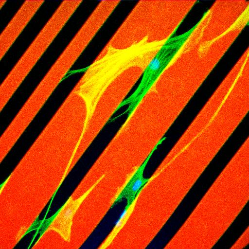
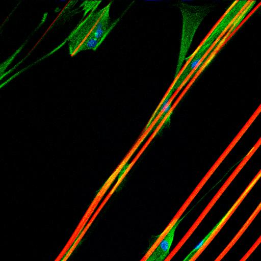
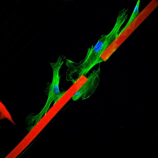
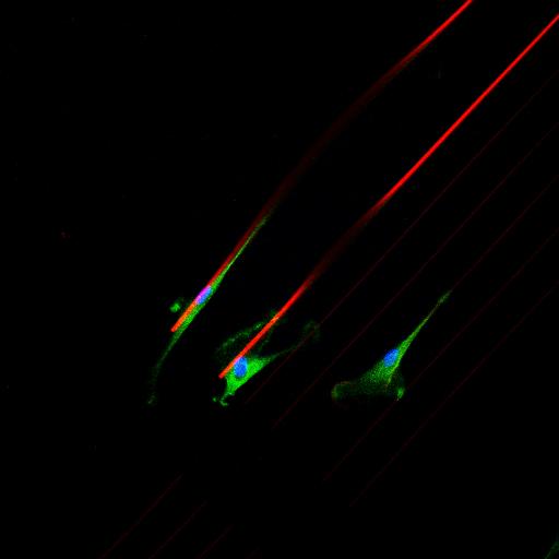
28 Sample 3: Photoresist/Si with gratings, dots, grids SMC grew on, and along the edge of the photoresist patterns most cells elongated on gratings 28


29 Sample 3 Dots around cells were moved toward the cells-cells grew on top of the dots might have pulled the dots along during the migration Thinner lines were deformed appeared to be caused by cell contraction and migration 29


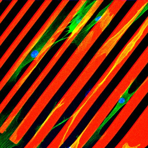
30 Sample 2: collagen coated SMC formed pattern-- two perpendicular lines 10x 30


31 Sample 1: PMMA/Si with submicron gratings SMC line-up and elongate along an axis (we cannot see the gratings) 31

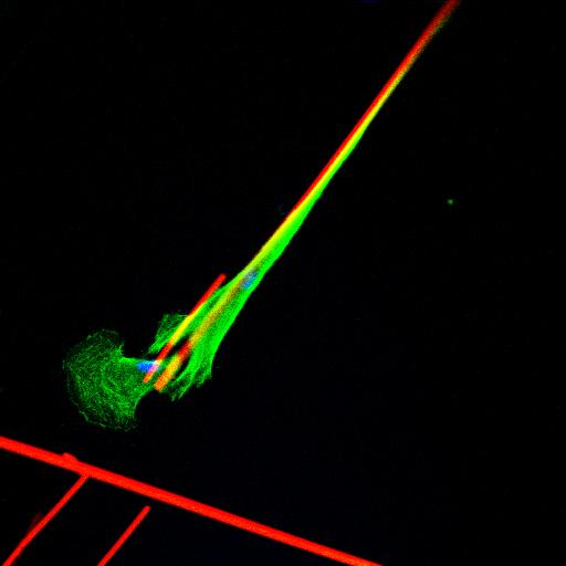
32 MC3T3-E1 behavior on NANO structures " Migration assay: 110 nm 32
33 MC3T3-E1 behavior on NANO structures " Migration assay: 350 nm 33

34 MC3T3-E1 behavior on NANO structures " IF images 34
Large-area patterning by roller-based nanoimprint lithography
 JOANNEUM RESEARCH Forschungsgesellschaft Institute MATERIALS, Weiz, Austria Large-area patterning by roller-based nanoimprint lithography Ursula Palfinger, Dieter Nees, Stephan Ruttloff, Markus Leitgeb,
Nanofabrication Prof. Stephen Y. Chou NanoStructure Laboratory
 Nanofabrication Prof. Stephen Y. Chou Department of Electrical Engineering Princeton University 1 Acknowledgment Dr. Paul Fischer Dr. Yun Wang Dr. Jay Guo Dr. Peter Klauss Dr. Jim Wang Dr. Longtin He Dr.
Superionic Solid State Stamping (S4)
") Superionic Solid State Stamping (S4) Lead Faculty Researcher: Placid Ferreira Department: Materials Science & Engineering Hsu et al, Nano Letters, 2007 1. Description: This dry, single step, electrochemical
Superionic Solid State Stamping (S4) Lead Faculty Researcher: Placid Ferreira Department: Materials Science & Engineering Hsu et al, Nano Letters, 2007 1. Description: This dry, single step, electrochemical
In-Situ Monitoring of Pattern Filling in Nano-Imprint Lithography Using Surface Plasmon Resonance
 Copyright 2011 American Scientific Publishers All rights reserved Printed in the United States of America Journal of Nanoscience and Nanotechnology Vol. 11, 1 6, 2011 In-Situ Monitoring of Pattern Filling
Vertically aligned Ni magnetic nanowires fabricated by diblock-copolymer-directed Al thin film anodization
 Vertically aligned Ni magnetic nanowires fabricated by diblock-copolymer-directed Al thin film anodization Researcher: Kunbae (Kevin) Noh, Graduate Student, MAE Dept. and CMRR Collaborators: Leon Chen,
Micro and nano structuring of carbon based materials for micro injection moulding and hot embossing
 Micro and nano structuring of carbon based materials for micro injection moulding and hot embossing Victor Usov, Graham Cross, Neal O Hara, Declan Scanlan, Sander Paulen, Chris de Ruijter, Daniel Vlasveld,
Metallic Antireflection Structures Made from Silver Ink by a Liquid Transfer Imprint Lithography Technique
 Journal of Photopolymer Science and Technology Volume 30, Number 5 (2017) 539-544 C 2017SPST Metallic Antireflection Structures Made from Silver Ink by a Liquid Transfer Imprint Lithography Technique Ichiro
Processing guidelines
 Processing guidelines mr-uvcur21 series UV-curable Polymer for UV-based Nanoimprint Lithography Characteristics mr-uvcur21 is a liquid UV-curable polymer system with low viscosity and high curing rate
Micro Injection Molding of Micro Fluidic Platform
 Micro Injection Molding of Micro Fluidic Platform S. C. Chen, J. A. Chang, Y. J. Chang and S. W. Chau Department of Mechanical Engineering, Chung Yuan University, Taiwan, ROC Abstract In this study, micro
Multiphoton lithography based 3D micro/nano printing Dr Qin Hu
 Multiphoton lithography based 3D micro/nano printing Dr Qin Hu EPSRC Centre for Innovative Manufacturing in Additive Manufacturing University of Nottingham Multiphoton lithography Also known as direct
Nanoimprint Lithography - Next Generation Nanopatterning Methods for Nanophotonics Fabrication
 14 Nanoimprint Lithography - Next Generation Nanopatterning Methods for Nanophotonics Fabrication Jukka Viheriälä, Tapio Niemi, Juha Kontio and Markus Pessa Optoelectronics Research Centre, Tampere University
TSV Processing and Wafer Stacking. Kathy Cook and Maggie Zoberbier, 3D Business Development
 TSV Processing and Wafer Stacking Kathy Cook and Maggie Zoberbier, 3D Business Development Outline Why 3D Integration? TSV Process Variations Lithography Process Results Stacking Technology Wafer Bonding
High-Speed Roll-to-Roll Nanoimprint Lithography on Flexible Plastic Substrates**
 COMMUNICATION DOI: 10.1002/adma.200702650 High-Speed Roll-to-Roll Nanoimprint Lithography on Flexible Plastic Substrates** By Se Hyun Ahn and L. Jay Guo* The ability of micro- to nanometer-scale patterning
Leveraging the Precision of Electroforming over Alternative Processes When Developing Nano-scale Structures
 VOLUME 4 - ELECTROFORMING Leveraging the Precision of over Alternative Processes When Developing Nano-scale Structures Electrical and mechanical component and subsystem designers generally have five techniques
Photolithography I ( Part 2 )
") 1 Photolithography I ( Part 2 ) Chapter 13 : Semiconductor Manufacturing Technology by M. Quirk & J. Serda Bjørn-Ove Fimland, Department of Electronics and Telecommunication, Norwegian University of Science
1 Photolithography I ( Part 2 ) Chapter 13 : Semiconductor Manufacturing Technology by M. Quirk & J. Serda Bjørn-Ove Fimland, Department of Electronics and Telecommunication, Norwegian University of Science
Antimicrobial Surfaces: Physical and Chemical Functionalization
 Antimicrobial Surfaces: Physical and Chemical Functionalization Iban Quintana EIBAR, May 3 th 2017 IK4-TEKNIKER 2017 Antimicrobial Surfaces Overview Passive Approach: Anti-biofouling Bactericidal Active
Integration of Block-Copolymer with Nano- Imprint Lithography: Pushing the Boundaries of Emerging Nano-Patterning Technology
 Integration of Block-Copolymer with Nano- Imprint Lithography: Pushing the Boundaries of Emerging Nano-Patterning Technology April 2010 update SNL Geoff Brennecka (PI) Bruce Burckel Matt George Jack Skinner
Step and Flash Imprint Lithography for sub-100nm Patterning
 Step and Flash Imprint Lithography for sub-100nm Patterning Matthew Colburn, Annette Grot, Marie Amistoso, Byung Jin Choi, Todd Bailey, John Ekerdt, S.V. Sreenivasan, James Hollenhorst, C. Grant Willson
D Eggenstein-Leopoldshafen, Germany 2 University of Karlsruhe (TH), Institute for Microstructure Technology (IMT),
, Institute for Microstructure Technology (IMT),") Sub-µ structured Lotus Surfaces Manufacturing M. Worgull 1, M. Heckele 1, T. Mappes 2, B. Matthis 1, G. Tosello 3, T. Metz 4, J. Gavillet 5, P. Koltay 4, H. N. Hansen 3 1 Forschungszentrum Karlsruhe (FZK),
Sub-µ structured Lotus Surfaces Manufacturing M. Worgull 1, M. Heckele 1, T. Mappes 2, B. Matthis 1, G. Tosello 3, T. Metz 4, J. Gavillet 5, P. Koltay 4, H. N. Hansen 3 1 Forschungszentrum Karlsruhe (FZK),
MCC. PMGI Resists NANO PMGI RESISTS OFFER RANGE OF PRODUCTS
 MCC PMGI RESISTS OFFER Sub.25µm lift-off processing Film thicknesses from 5µm Choice of resin blends for optimal undercut control High thermal stability Superior adhesion to Si, NiFe, GaAs, InP
micro resist technology
 Characteristics Processing guidelines Negative Tone Photoresist Series ma-n 2400 ma-n 2400 is a negative tone photoresist series designed for the use in micro- and nanoelectronics. The resists are available
Lecture 6. Through-Wafer Interconnect. Agenda: Through-wafer Interconnect Polymer MEMS. Through-Wafer Interconnect -1. Through-Wafer Interconnect -2
 Agenda: EEL6935 Advanced MEMS (Spring 2005) Instructor: Dr. Huikai Xie Lecture 6 Through-wafer Interconnect EEL6935 Advanced MEMS 2005 H. Xie 1/21/2005 1 Motivations: Wafer-level packaging CMOS 3D Integration
EXCIMER LASER ANNEALING FOR LOW- TEMPERATURE POLYSILICON THIN FILM TRANSISTOR FABRICATION ON PLASTIC SUBSTRATES
 EXCIMER LASER ANNEALING FOR LOW- TEMPERATURE POLYSILICON THIN FILM TRANSISTOR FABRICATION ON PLASTIC SUBSTRATES G. Fortunato, A. Pecora, L. Maiolo, M. Cuscunà, D. Simeone, A. Minotti, and L. Mariucci CNR-IMM,
HIGH-THROUGHPUT, CONTINUOUS NANOPATTERNING TECHNOLOGIES FOR DISPLAY AND ENERGY APPLICATIONS
 HIGH-THROUGHPUT, CONTINUOUS NANOPATTERNING TECHNOLOGIES FOR DISPLAY AND ENERGY APPLICATIONS by Se Hyun Ahn A dissertation submitted in partial fulfillment of the requirements for the degree of Doctor of
Sub-5 nm Structures Process Development and Fabrication Over Large Areas
 A S Jugessur,, 2017, 1:1 SciFed Nanotech Research Letters Research Article Open Access Sub-5 nm Structures Process Development and Fabrication Over Large Areas * A S Jugessur * University of Iowa Microfabrication
Photoresist Coat, Expose and Develop Laboratory Dr. Lynn Fuller
 ROCHESTER INSTITUTE OF TECHNOLOGY MICROELECTRONIC ENGINEERING Photoresist Coat, Expose and Develop Laboratory Dr. Lynn Fuller Webpage: http://www.rit.edu/lffeee 82 Lomb Memorial Drive Rochester, NY 14623-5604
Micropatterning and casting PEDOT-PSS /DMSO layers
 Micropatterning and casting PEDOT-PSS /DMSO layers Benoît Charlot, Gilbert Sassine, Alexandra Garraud, Alain Giani, Philippe Combette IES Institut d Electronique du Sud CNRS Université Montpellier II Place&E.&Bataillon,&34095&Montpellier&7&France&
NIL defect performance toward High volume mass production
 NIL defect performance toward High volume mass production Masayuki Hatano a, Kei Kobayashi a, Hiroyuki Kashiwagi a, Hiroshi Tokue a, Takuya Kono a, Nakasugi Tetsuro a, Eun Hyuk Choi b, Wooyung Jung b a
From microelectronics down to nanotechnology.
 From microelectronics down to nanotechnology sami.franssila@tkk.fi Contents Lithography: scaling x- and y-dimensions MOS transistor physics Scaling oxide thickness (z-dimension) CNT transistors Conducting
EXPLORING VACUUM CASTING TECHNIQUES FOR MICRON AND SUBMICRON FEATURES. Campus Ker Lann, av Robert Schumann Bruz, France
 EXPLORING VACUUM CASTING TECHNIQUES FOR MICRON AND SUBMICRON FEATURES M. Denoual *, P. Mognol **, B. Lepioufle * * Biomis-SATIE ENS-Cachan antenne de Bretagne, Campus Ker Lann, av Robert Schumann 35170
LOW TEMPERATURE PHOTONIC SINTERING FOR PRINTED ELECTRONICS. Dr. Saad Ahmed XENON Corporation November 19, 2015
 LOW TEMPERATURE PHOTONIC SINTERING FOR PRINTED ELECTRONICS Dr. Saad Ahmed XENON Corporation November 19, 2015 Topics Introduction to Pulsed Light Photonic sintering for Printed Electronics R&D Tools for
MCC. NANO PMMA and Copolymer
 MCC PRODUCT ATTRIBUTES NANO and Submicron linewidth control (polymethyl methacrylate) is a versatile polymeric material that is well suited Sub 0.1µm imaging for many imaging and non-imaging microelectronic
Processing guidelines. Negative Tone Photoresist Series ma-n 2400
 Characteristics Processing guidelines Negative Tone Photoresist Series ma-n 2400 ma-n 2400 is a negative tone photoresist series designed for the use in micro- and nanoelectronics. The resists are available
Photonic Drying Pulsed Light as a low Temperature Sintering Process
 Photonic Drying Pulsed Light as a low Temperature Sintering Process Lou Panico Xenon Corporation W E S T E R N M I C H I G A N U N I V E R S I T Y PRESENTATION OVERVIEW What is Printed Electronics Materials
Novel Spin on Planarization Technology by Photo Curing SOC (P-SOC)
") Journal of Photopolymer Science and Technology Volume 3, Number 3 (17) 373-378 C 17SPST Technical Paper Novel Spin on Planarization Technology by Photo Curing (P-) Takafumi Endo*, Rikimaru Sakamoto, Keisuke
Journal of Photopolymer Science and Technology Volume 3, Number 3 (17) 373-378 C 17SPST Technical Paper Novel Spin on Planarization Technology by Photo Curing (P-) Takafumi Endo*, Rikimaru Sakamoto, Keisuke
The Effect of Hydrophobic Patterning on Micromolding of Aqueous-Derived Silk Structures
 The Effect of Hydrophobic Patterning on Micromolding of Aqueous-Derived Silk Structures Konstantinos Tsioris 1, Robert D White 1, David L Kaplan 2, and Peter Y Wong 1 1 Mechanical Engineering, Tufts University,
Fabrication Techniques for Thin-Film Silicon Layer Transfer
 Fabrication Techniques for Thin-Film Silicon Layer Transfer S. L. Holl a, C. A. Colinge b, S. Song b, R. Varasala b, K. Hobart c, F. Kub c a Department of Mechanical Engineering, b Department of Electrical
EE40 Lec 22. IC Fabrication Technology. Prof. Nathan Cheung 11/19/2009
 Suggested Reading EE40 Lec 22 IC Fabrication Technology Prof. Nathan Cheung 11/19/2009 300mm Fab Tour http://www-03.ibm.com/technology/manufacturing/technology_tour_300mm_foundry.html Overview of IC Technology
125nXT Series. EMD PeRFoRmaNce MaTeRIaLs. technical datasheet. Photopolymer Negative Tone Photoresists APPLICATION TYPICAL PROCESS THICKNESS GRADES
 EMD PeRFoRmaNce MaTeRIaLs technical datasheet AZ 125nXT Series Photopolymer Negative Tone Photoresists APPLICATION Thick photopolymer photoresists featuring aspect ratios and photospeed not possible with
FABRICATION FOR MICRO PATTERNS OF NICKEL MATRIX DIAMOND COMPOSITES USING THE COMPOSITE ELECTROFORMING AND UV- LITHOGRAPHY
 16 TH INTERNATIONAL CONFERENCE ON COMPOSITE MATERIALS FABRICATION FOR MICRO PATTERNS OF NICKEL MATRIX DIAMOND COMPOSITES USING THE COMPOSITE ELECTROFORMING AND UV- LITHOGRAPHY Tsung-Han Yu, Shenq-Yih Luo,
Fabrication of aligned metallic structures based on block copolymer lithography
 88 Fabrication of aligned metallic structures based on block copolymer lithography Yusuke Takahashi Department ofmicroelectronic Engineering, Rochester Institute of Technology, 82 Lomb Memorial Dr., Rochester,
PARAMETER EFFECTS FOR THE GROWTH OF THIN POROUS ANODIC ALUMINUM OXIDES
 10.1149/1.2794473, The Electrochemical Society PARAMETER EFFECTS FOR THE GROWTH OF THIN POROUS ANODIC ALUMINUM OXIDES S. Yim a, C. Bonhôte b, J. Lille b, and T. Wu b a Dept. of Chem. and Mat. Engr., San
THIN FILM THICKNESS MEASUREMENT FOR EVALUATION OF RESIDUAL LAYER OF NANO-IMPRINT LITHOGRAPHY USING NEAR-FIELD OPTICS
 9 th INTERNATIONAL SYMPOSIUM ON MEASUREMENT AND QUALITY CONTROL (9 th ISMQC) November 21 24, 27, IIT Madras THIN FILM THICKNESS MEASUREMENT FOR EVALUATION OF RESIDUAL LAYER OF NANO-IMPRINT LITHOGRAPHY
Electron Microscopy Sciences Industry Road. P.O. Box 550. Hatfield, PA Introduction. DuraSiNTM
 DuraSiNTM Electron Microscopy Sciences Introduction DuraSiN TM Film and Mesh products have revolutionized the way samples are prepared for and analyzed in the transmission electron microscope. DuraSiN
Towards scalable fabrication of high efficiency polymer solar cells
 Towards scalable fabrication of high efficiency polymer solar cells Hui Joon Park 2*, Myung-Gyu Kang 1**, Se Hyun Ahn 3, Moon Kyu Kang 1, and L. Jay Guo 1,2,3 1 Department of Electrical Engineering and
Lecture 10: MultiUser MEMS Process (MUMPS)
") MEMS: Fabrication Lecture 10: MultiUser MEMS Process (MUMPS) Prasanna S. Gandhi Assistant Professor, Department of Mechanical Engineering, Indian Institute of Technology, Bombay, 1 Recap Various VLSI based
MEMS: Fabrication Lecture 10: MultiUser MEMS Process (MUMPS) Prasanna S. Gandhi Assistant Professor, Department of Mechanical Engineering, Indian Institute of Technology, Bombay, 1 Recap Various VLSI based
Advanced developer-soluble gap-fill materials and applications
 Advanced developer-soluble gap-fill materials and applications Runhui Huang, Dan Sullivan, Anwei Qin, Shannon Brown Brewer Science, Inc., 2401 Brewer Dr., Rolla, MO, USA, 65401 ABSTRACT For the via-first
Uncrosslinked SU-8 as a sacrificial material
 INSTITUTE OFPHYSICS PUBLISHING JOURNAL OF MICROMECHANICS AND MICROENGINEERING J. Micromech. Microeng. 15 (2005) N1 N5 doi:10.1088/0960-1317/15/1/n01 TECHNICAL NOTE Uncrosslinked as a sacrificial material
Nanostructure Fabrication by Nanoimprint Lithography and its Applications
 Nanostructure Fabrication by Nanoimprint Lithography and its Applications Those slides summarized several research projects I carried out at National Research Council (NRC) during 2003-2008 Bo Cui CNRC-Industrial
Thin Wafers Bonding & Processing
 Thin Wafers Bonding & Processing A market perspective 2012 Why New Handling Technologies Consumer electronics is today a big driver for smaller, higher performing & lower cost device configurations. These
Lab #2 Wafer Cleaning (RCA cleaning)
") Lab #2 Wafer Cleaning (RCA cleaning) RCA Cleaning System Used: Wet Bench 1, Bay1, Nanofabrication Center Chemicals Used: H 2 O : NH 4 OH : H 2 O 2 (5 : 1 : 1) H 2 O : HF (10 : 1) H 2 O : HCl : H 2 O 2
Lab #2 Wafer Cleaning (RCA cleaning) RCA Cleaning System Used: Wet Bench 1, Bay1, Nanofabrication Center Chemicals Used: H 2 O : NH 4 OH : H 2 O 2 (5 : 1 : 1) H 2 O : HF (10 : 1) H 2 O : HCl : H 2 O 2
Mold Fabrication for 3D Dual Damascene Imprinting
 Nanoscale Res Lett (2010) 5:545 549 DOI 10.1007/s11671-010-9540-2 SPECIAL ISSUE ARTICLE Mold Fabrication for 3D Dual Damascene Imprinting S. M. Saydur Rahman Bo Cui Received: 11 September 2009 / Accepted:
Wafer-to-Wafer Bonding and Packaging
 Wafer-to-Wafer Bonding and Packaging Dr. Thara Srinivasan Lecture 25 Picture credit: Radant MEMS Reading Lecture Outline Senturia, S., Chapter 17, Packaging. Schmidt, M. A. Wafer-to-Wafer Bonding for Microstructure
Nanocoating close to the market
 Nanocoating close to the market Moritz Graf zu Eulenburg Introduction Market overview Overview of most important coating aspects Description of different coating systems Description of different drying
Positive Photoresists
 Positive Photoresists Gesellschaft für chemische Materialien spezieller Photoresistsysteme mbh Positive Photoresists map 1200 series Thick resists map 1275, map 1275 HV Unique features of the positive
Soft-lithography for Preparing Patterned Liquid Crystal Orientations
 2007 KIDS Soft-lithography for Preparing Patterned Liquid Crystal Orientations Hak-Rin Kim **a, Jong-Wook Jung **a, Min-Soo Shin **a, Myung-Eun Kim a, You-Jin Lee **a, and Jae-Hoon Kim *b Abstract We demonstrate
Supporting Information
 Supporting Information Fast-Response, Sensitivitive and Low-Powered Chemosensors by Fusing Nanostructured Porous Thin Film and IDEs-Microheater Chip Zhengfei Dai,, Lei Xu,#,, Guotao Duan *,, Tie Li *,,
Precise Ion and Electron Beam Processing for Nano-Structuring
 Precise Ion and Electron Beam Processing for Nano-Structuring Regina Korntner, Hans Loeschner and Elmar Platzgummer Vienna, Austria 1 Outline Short Introduction to IMS Technology Introduction History of
Novel Materials and Activities for Next Generation Package. Hitachi Chemical., Co.Ltd. Packaging Solution Center Hiroaki Miyajima
 Novel Materials and Activities for Next Generation Package Hitachi Chemical., Co.Ltd. Packaging Solution Center Hiroaki Miyajima 1. Activities of Packaging Solution Center 2. Novel Materials for Next Gen.
Micro-Electro-Mechanical Systems (MEMS) Fabrication. Special Process Modules for MEMS. Principle of Sensing and Actuation
 Fabrication. Special Process Modules for MEMS. Principle of Sensing and Actuation") Micro-Electro-Mechanical Systems (MEMS) Fabrication Fabrication Considerations Stress-Strain, Thin-film Stress, Stiction Special Process Modules for MEMS Bonding, Cavity Sealing, Deep RIE, Spatial forming
Micro-Electro-Mechanical Systems (MEMS) Fabrication Fabrication Considerations Stress-Strain, Thin-film Stress, Stiction Special Process Modules for MEMS Bonding, Cavity Sealing, Deep RIE, Spatial forming
Via Fill in Small Trenches using Hot Aluminum Process. By Alice Wong
 Via Fill in Small Trenches using Hot Aluminum Process By Alice Wong Goals for Project Good Via Fill in Small contact holes using hot aluminum process Be able to get good images of the contact holes using
Optimizing spray coater process parameters
 Optimizing spray coater process parameters Dr. Eleonora Storace, Florian Palitschka, Dr. Dietrich Tönnies SUSS MicroTec Lithography GmbH Germany Published in the SUSS report 01/2014 E-mail: info@suss.com
Presented at the 28th European PV Solar Energy Conference and Exhibition, 30 September 4 October, 2013, Paris, France
 INTEGRATING DIFFRACTIVE REAR SIDE STRUCTURES FOR LIGHT TRAPPING INTO CRYSTALLINE SILICON SOLAR CELLS J. Eisenlohr 1*, H. Hauser 1, J. Benick 1, A. Mellor 2, B. Bläsi 1, J.C. Goldschmidt 1, M. Hermle 1
PROCESSING OF INTEGRATED CIRCUITS
 PROCESSING OF INTEGRATED CIRCUITS Overview of IC Processing (Part I) Silicon Processing Lithography Layer Processes Use in IC Fabrication (Part II) Integrating the Fabrication Steps IC Packaging (Part
Advances in Intense Pulsed Light Solutions For Display Manufacturing. XENON Corporation Dr. Saad Ahmed Japan IDW 2016
 Advances in Intense Pulsed Light Solutions For Display Manufacturing XENON Corporation Dr. Saad Ahmed Japan IDW 2016 Talk Outline Introduction to Pulsed Light Applications in Display UV Curing Applications
EV Group 300mm Wafer Bonding Technology July 16, 2008
 EV Group 300mm Wafer Bonding Technology July 16, 2008 EV Group in a Nutshell st Our philosophy Our mission in serving next generation application in semiconductor technology Equipment supplier for the
Hybrid BARC approaches for FEOL and BEOL integration
 Hybrid BARC approaches for FEOL and BEOL integration Willie Perez a, Stephen Turner a, Nick Brakensiek a, Lynne Mills b, Larry Wilson b, Paul Popa b a Brewer Science, Inc., 241 Brewer Dr., Rolla, MO 6541
Mater. Res. Soc. Symp. Proc. Vol Materials Research Society
 Mater. Res. Soc. Symp. Proc. Vol. 940 2006 Materials Research Society 0940-P13-12 A Novel Fabrication Technique for Developing Metal Nanodroplet Arrays Christopher Edgar, Chad Johns, and M. Saif Islam
Chips Face-up Panelization Approach For Fan-out Packaging
 Chips Face-up Panelization Approach For Fan-out Packaging Oct. 15, 2015 B. Rogers, D. Sanchez, C. Bishop, C. Sandstrom, C. Scanlan, TOlson T. REV A Background on FOWLP Fan-Out Wafer Level Packaging o Chips
Low Pressure Molding Overview. Henkel Electronics
 Low Pressure Molding Overview Henkel Electronics Agenda 1 Technology 2 Process 3 Solutions 2 February 25, 2016 Low Pressure Molding Overview Agenda TECHNOMELT Low Pressure Molding 1. Overview of Technology
High-throughput three-dimensional (3D) lithographic microfabrication in biomedical applications
 lithographic microfabrication in biomedical applications") High-throughput three-dimensional (3D) lithographic microfabrication in biomedical applications The MIT Faculty has made this article openly available. Please share how this access benefits you. Your story
High-throughput three-dimensional (3D) lithographic microfabrication in biomedical applications The MIT Faculty has made this article openly available. Please share how this access benefits you. Your story
Filling and Planarizing Deep Trenches with Polymeric Material for Through-Silicon Via Technology
 Filling and Planarizing Deep Trenches with Polymeric Material for Through-Silicon Via Technology R.K. Trichur, M. Fowler, J.W. McCutcheon, and M. Daily Brewer Science, Inc. 2401 Brewer Drive Rolla, MO
Plasma Etching Rates & Gases Gas ratios affects etch rate & etch ratios to resist/substrate
 Plasma Etching Rates & Gases Gas ratios affects etch rate & etch ratios to resist/substrate Development of Sidewalls Passivating Films Sidewalls get inert species deposited on them with plasma etch Creates
Microcontact Printing Procedures for Adhesive and Conductive Epoxies
 Microcontact Printing Procedures for Adhesive and Conductive Epoxies This objective was accomplished through a formal record of the procedures to deliver a stamped product which met the benchmark mechanical,
Delamination of Thin Films Using Laser Induced Stress Waves
 Center for Nanoscale Chemical-Electrical-Mechanical Manufacturing Systems Delamination of Thin Films Using Laser Induced Stress Waves Undergraduate Researcher Angelica Anne Vargas, Research Experience
Applications of High-Performance MEMS Pressure Sensors Based on Dissolved Wafer Process
 Applications of High-Performance MEMS Pressure Sensors Based on Dissolved Wafer Process Srinivas Tadigadapa and Sonbol Massoud-Ansari Integrated Sensing Systems (ISSYS) Inc., 387 Airport Industrial Drive,
Materials Characterization for Stress Management
 Materials Characterization for Stress Management Ehrenfried Zschech, Fraunhofer IZFP Dresden, Germany Workshop on Stress Management for 3D ICs using TSVs San Francisco/CA, July 13, 2010 Outline Stress
Metallization deposition and etching. Material mainly taken from Campbell, UCCS
 Metallization deposition and etching Material mainly taken from Campbell, UCCS Application Metallization is back-end processing Metals used are aluminum and copper Mainly involves deposition and etching,
SU Permanent Epoxy Negative Photoresist PROCESSING GUIDELINES FOR:
 SU-8 2000 Permanent Epoxy Negative Photoresist PROCESSING GUIDELINES FOR: SU-8 2100 and SU-8 2150 www.microchem.com SU-8 2000 is a high contrast, epoxy based photoresist designed for micromachining and
Technology. Semiconductor Manufacturing. Hong Xiao INTRODUCTION TO SECOND EDITION SPIE PRESS
 INTRODUCTION TO Semiconductor Manufacturing Technology SECOND EDITION Hong Xiao TECHNISCHE INFORMATIONSBiBUOTHEK UNIVERSITATSBIBLIOTHEK HANNOVER SPIE PRESS Bellingham,Washington USA Contents Preface to
Process Variability in Micro-Embossing
 Process Variability in Micro-Embossing David Hardt, Bala Ganesan, Matthew Dirckx, Grant Shoji, Kunal Thaker and Wang Qi Laboratory for Manufacturing and Productivity Massachusetts Institute of Technology
Deep Lithography for Microfabrication
 Deep Lithography for Microfabrication Part 2: UV Deep Lithography (UVDL) Luiz O. S. Ferreira Mechanical Engineering Faculty Campinas State University UNICAMP Campinas SP - BRAZIL lotavio@fem.unicamp.br
Lecture 5. SOI Micromachining. SOI MUMPs. SOI Micromachining. Silicon-on-Insulator Microstructures. Agenda:
 EEL6935 Advanced MEMS (Spring 2005) Instructor: Dr. Huikai Xie SOI Micromachining Agenda: SOI Micromachining SOI MUMPs Multi-level structures Lecture 5 Silicon-on-Insulator Microstructures Single-crystal
The Effects of Defects on the Moisture-Barrier Performance of Clear Coatings on Polymer Substrates.
 AIMCAL, CHARLESTON, SC, 2013 The Effects of Defects on the Moisture-Barrier Performance of Clear Coatings on Polymer Substrates. The National Centre for Printed Electronics ALF part SMITH of Centre for
Enabling Technology in Thin Wafer Dicing
 Enabling Technology in Thin Wafer Dicing Jeroen van Borkulo, Rogier Evertsen, Rene Hendriks, ALSI, platinawerf 2G, 6641TL Beuningen Netherlands Abstract Driven by IC packaging and performance requirements,
Copyright. Stephen Christopher Johnson
 Copyright by Stephen Christopher Johnson 2005 The Dissertation Committee for Stephen Christopher Johnson Certifies that this is the approved version of the following dissertation: Step and Flash Imprint
Nanotechnological Applications of Biomolecular Motor Systems. Stefan Diez Max-Planck-Institute of Molecular Cell Biology and Genetics Dresden
 Nanotechnological Applications of Biomolecular Motor Systems Stefan Diez Max-Planck-Institute of Molecular Cell Biology and Genetics Dresden Max-Planck-Institute of Molecular Cell Biology and Genetics
Ultra Fine Pitch Bumping Using e-ni/au and Sn Lift-Off Processes
 Ultra Fine Pitch Bumping Using e-ni/au and Sn Lift-Off Processes Andrew Strandjord, Thorsten Teutsch, and Jing Li Pac Tech USA Packaging Technologies, Inc. Santa Clara, CA USA 95050 Thomas Oppert, and
MICROFABRICATION OF OPTICALLY ACTIVE InO X MICROSTRUCTURES BY ULTRASHORT LASER PULSES
 Journal of Optoelectronics and Advanced Materials Vol. 4, No. 3, September 2002, p. 809-812 MICROFABRICATION OF OPTICALLY ACTIVE InO X MICROSTRUCTURES BY ULTRASHORT LASER PULSES Foundation for Research
Vacuum casting, a new answer for manufacturing biomicrosystems
 1 Vacuum casting, a new answer for manufacturing biomicrosystems M Denoual 1 *, P Mognol 2, and B Lepioufle 1 1 Biomis-SATIE ENS-Cachan antenne de Bretagne, Bruz, France 2 IRCCyN Nantes, France The manuscript
NTT-AT Optical Adhesives Lineup. Adhesives / Resins and Sealants for Optical Component Assembly
 NTT-AT Optical Adhesives Lineup Adhesives / Resins and Sealants for Optical Component Assembly The adhesive technology used in optical communications is one of the key technologies we offer. Ask us anything
ME 189 Microsystems Design and Manufacture. Chapter 9. Micromanufacturing
 ME 189 Microsystems Design and Manufacture Chapter 9 Micromanufacturing This chapter will offer an overview of the application of the various fabrication techniques described in Chapter 8 in the manufacturing
A Lab-on-Chip System for direct SNP sensing from human blood
 A LabonChip System for direct SP sensing from human blood Ichiro Yamashita 1,3, Paolo Fiorini 2 1 Advanced Technology Research Laboratory, Panasonic corp. 34 Hikaridai, Seikacho, Sorakugun, Kyoto 6190237,
3D technologies for integration of MEMS
 3D technologies for integration of MEMS, Fraunhofer Institute for Electronic Nano Systems Folie 1 Outlook Introduction 3D Processes Process integration Characterization Sample Applications Conclusion Folie
Magnetic Force Microscopy: nanoscale magnetic imaging and lithography
 NTEGRA Aura Magnetic Force Microscopy: nanoscale magnetic imaging and lithography The principle of Magnetic Force Microscopy (MFM) is based on the detection of the interaction between the sample and a
Assembly of Mechanically Compliant Interfaces between Optical Fibers and Nanophotonic Chips
 Assembly of Mechanically Compliant Interfaces between Optical Fibers and Nanophotonic Chips T. Barwicz, Y. Taira, H. Numata, N. Boyer, S. Harel, S. Kamlapurkar, S. Takenobu, S. Laflamme, S. Engelmann,
NANO SCRATCH TESTING OF THIN FILM ON GLASS SUBSTRATE
 NANO SCRATCH TESTING OF THIN FILM ON GLASS SUBSTRATE Prepared by Jesse Angle 6 Morgan, Ste156, Irvine CA 92618 P: 949.461.9292 F: 949.461.9232 nanovea.com Today's standard for tomorrow's materials. 2010
TSV Interposer Process Flow with IME 300mm Facilities
 TSV Interposer Process Flow with IME 300mm Facilities Property of Institute of Microelectronics (IME)-Singapore August 17, 2012 Outline 1. TSV interposer (TSI) cross sectional schematic TSI with BEOL,
3D Laser Lithography in Biotechnology and Medical Technology
 3D Laser Lithography in Biotechnology and Medical Technology High-Precision, Piezo-Based Nanopositioning Systems Advance Technology Page 1 of 6 Laser technology makes it possible to create even very complex
Nano- And Micro-Filled Conducting Adhesives For Z-axis Interconnects
 Nano- And Micro-Filled Conducting Adhesives For Z-axis Interconnects We take a look at micro-filled epoxy-based conducting adhesives modified with nanoparticles for z- axis interconnections, especially