Laser Micromachining - Market Focus. Dr. Andrew Kearsley
|
|
|
- Samson Hood
- 6 years ago
- Views:
Transcription
1 Laser Micromachining - Market Focus Dr. Andrew Kearsley Oxford Lasers Ltd. Moorbrook Park, Didcot OX11 7HP andrew.kearsley@oxfordlasers.com 5th CIR HVM-UK: South East Conference Harwell, 17 November 2005
2 Overview of Talk Introduction to Oxford Lasers Characteristics of Laser Micromachining Laser micromachining systems High Value Applications of Laser Micromachining Future challenges
3 Oxford Lasers Founded 1977 as spin off from Oxford University Based in Didcot, Oxfordshire Two divisions: Imaging and Industrial Imaging: integrates laser (strobe light), camera, computer, software, optics and applications knowledge into imaging systems. Industrial: integrates lasers, beam delivery, beam manipulation optics, work handling, control and process knowledge into micromachining systems Main geographic markets: UK, USA and Japan Subsidiary in USA, just north of Boston
4 Industrial Division - Core Strengths Knowledge of wide range of lasers. Knowledge of work handling, imaging, optics etc required for a system. Knowledge of wide range of laser applications. Knowledge of laser processing techniques. Ability to innovate / develop new processes. Ability to match customer requirements and laser process / system.
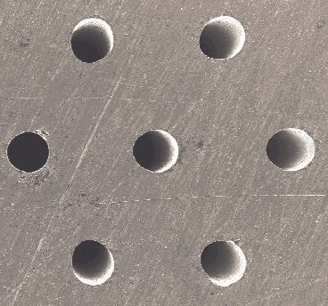
5 Characteristics of Laser Micromachining Very high precision (< 1 micron accuracy). Very little damage or stress on substrate. Relatively slow. Relatively expensive and tends to cost more than traditional techniques. Target markets have to have high value added by the use of laser micromachining.
6 Services offered Sample production Process development Pilot or low/medium volume production System manufacture Additional production capacity during surges in demand Long term support
7 Sales Process Marketing Customer Enquiry Laser Micromachining Feasibility Study metals, ceramics, polymers, glass,semiconductors,composite System definition and proposal and / or Pilot Production System Sale System Design, Build & Commissioning


8 Micromachining Systems Fully automated laser micromachining system Laser Proprietary Optical Trepanning System 5-axis part positioning Material handling systems (options) User-friendly pc interface
9 Which Laser to use? (Quality) (Proc.Speed) Laser Wavelength Laser Pulse Width Laser Beam Profile Laser Power Laser Rep.Rate Laser Focussability Important Parameters hole size hole aspect ratio feature quality processing speed cost per hole


10 Examples of Materials Silicon Nitride 90 m Ø, 500 m thick Steel m Ø, 100 m thick Silicon 125 m Ø, 350 m thick Upilex Polyimide 500 m thick
11 Industrial Laser Micromachining Applications Wide variety of markets including: Semi/Microelectronics Inkjet Printer Nozzle PCB via interconnects IC Test Vertical Probe Card Optical Switching Heat management in PCB packaging Automotive Fuel-Injection Nozzle Fuel Filter Car brake sensors Con-rod lubrication Aerospace/Defence Turbine component cooling Engine Silencing Missile guidance Aerofoil laminar flow BioMedical MEMS Catheter Sensors Aerosol Spray Atomisers DNA Sampling Vaccine production Lab-on-a-Chip Environment/Energy Toxic Gas Sensors Solar Cell Technology Fuel Cell Particulate Filters Other Food Packaging Gem Stone drilling Digital Fingerprinting

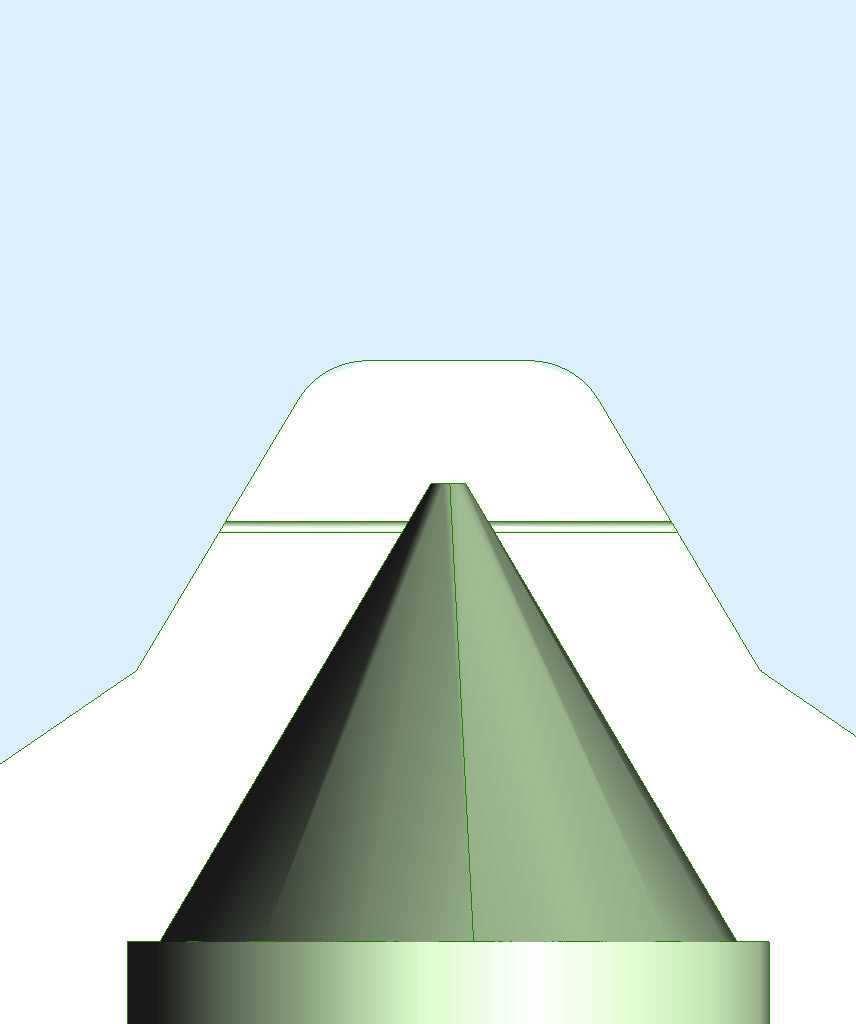
12 IC Vertical Test Probe Card Vertical probe heads are used for IC electrical testing prior to packaging. They require microholes to guide the contacting wires. Laser drilling of the guide plates allows high packing density with smaller hole sizes and provides flexibility, high processing speed Guide Plates Probe wires IC test wafer Probe Head Materials silicon ceramics (Al 2 O 3, Si 3 N 4 & others) plastics (PI) Hole Geometry Hole size : µm diameter Hole shape : square, circular, elliptical Hole Cylindricity : parallel or tapered Wafer thickness : m Technology challenges Hole position accuracy Speed of drilling Taper angle control tolerance Toolpath flexibility, any hole shape

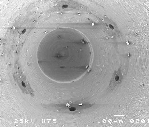
![entrance m] Exit Diameter [](/docs-images/77/75963085/images/13-5.jpg "Hole Size Repeatability 50 49")

13 IC Vertical Test Probe Card Si 3 N m thick, 511nm entrance m] Exit Diameter [ Hole Size Repeatability Hole Number exit 90 mø Silicon 50 m square
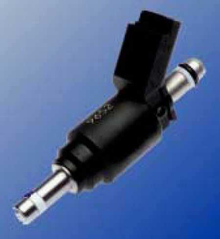
14 Fuel-Injection Diesel-injection nozzle Gasoline-injection nozzle Fuel feed Injection hole valve
15 Future Trends in Laser Micromachining Better Resolution (shorter wavelength, shorter pulses) Lower Production Cost (process speed, high rep.rate, high power) Better Quality (shorter pulses, faster motion control) More Complex Materials (multi-wavelength laser systems) Industrial Robustness (compact, fully diode-pumped laser systems)
16 Future Challenges Getting market to appreciate value of services provided. Protecting intellectual property, often know-how rather than patents. Maintain margins as applications take off and customers require multiple systems. Maintain markets as laser micromachining knowledge becomes widespread and migrates to lower cost economies. Identify new volume applications.
High Throughput Laser Processing of Guide Plates for Vertical Probe Cards Rouzbeh Sarrafi, Dana Sercel, Sean Dennigan, Joshua Stearns, Marco Mendes
 High Throughput Laser Processing of Guide Plates for Vertical Probe Cards Rouzbeh Sarrafi, Dana Sercel, Sean Dennigan, Joshua Stearns, Marco Mendes IPG Photonics - Microsystems Division Outline Introduction
Laser MicroJet. a technology for - prototyping - design innovation - mass customization - small / mid-sized manufacturing runs.
 Innovative Laser Systems Laser MicroJet a technology for - prototyping - design innovation - mass customization - small / mid-sized manufacturing runs Eric Krause EPMT EPHJ Swissphotonics seminar June
Laser Micromachining for Industrial Applications and R&D. 3D-Micromac AG. Symposium on Smart Integrated Systems in Chemnitz. 3D-Micromac AG
 3D-Micromac AG Symposium on Smart Integrated Systems in Chemnitz 1 1 microdice - TLS-Dicing for separation of SiC 2 microprep - for high-throughput microstructure diagnostics 3 About 3D-Micromac AG 2 microdice
Improvement of Laser Fuse Processing of Fine Pitch Link Structures for Advanced Memory Designs
 Improvement of Laser Fuse Processing of Fine Pitch Link Structures for Advanced Memory Designs Joohan Lee, Joseph J. Griffiths, and James Cordingley GSI Group Inc. 60 Fordham Rd. Wilmington, MA 01887 jlee@gsig.com
Confocal Microscopy of Electronic Devices. James Saczuk. Consumer Optical Electronics EE594 02/22/2000
 Confocal Microscopy of Electronic Devices James Saczuk Consumer Optical Electronics EE594 02/22/2000 Introduction! Review of confocal principles! Why is CM used to examine electronics?! Several methods
Innovative Laser Processing Technologies
 Innovative Laser Processing Technologies Reinhard Ferstl Director Sales & Marketing EMEA / Asia Corning Laser Technologies September 21, 2016 2016 Corning Incorporated Corning Market Segments and Additional
Interlayer Dielectric (ILD) Cracking Mechanisms and their Effects on Probe Processes. Daniel Stillman, Daniel Fresquez Texas Instruments Inc.
 Cracking Mechanisms and their Effects on Probe Processes. Daniel Stillman, Daniel Fresquez Texas Instruments Inc.") Interlayer Dielectric (ILD) Cracking Mechanisms and their Effects on Probe Processes Daniel Stillman, Daniel Fresquez Texas Instruments Inc. Outline Probe Optimization Why is it needed? Objective and obstacles
Interlayer Dielectric (ILD) Cracking Mechanisms and their Effects on Probe Processes Daniel Stillman, Daniel Fresquez Texas Instruments Inc. Outline Probe Optimization Why is it needed? Objective and obstacles
Tackling the optical interconnection challenge for the Integrated Photonics Revolution
 Tackling the optical interconnection challenge for the Integrated Photonics Revolution Dr. Ir. TU Delft, Precision and Microsystems Engineering m.tichem@tudelft.nl Microfabrication and MEMS Si microfabrication
MANUFACTURE AND REPAIR OF AERO ENGINE COMPONENTS USING LASER TECHNOLOGY (INVITED PAPER) Paper (405)
 Paper (405)") Proceedings of the 3 rd Pacific International Conference on Application of Lasers and Optics 2008 MANUFACTURE AND REPAIR OF AERO ENGINE COMPONENTS USING LASER TECHNOLOGY (INVITED PAPER) Paper (405) Ingomar
Proceedings of the 3 rd Pacific International Conference on Application of Lasers and Optics 2008 MANUFACTURE AND REPAIR OF AERO ENGINE COMPONENTS USING LASER TECHNOLOGY (INVITED PAPER) Paper (405) Ingomar
Fiber laser welding system. Welding
 Fiber laser welding system Welding A new era of laser welding Multi-functional, high speed and high grade welding Integrated processing from 3D CAD/CAM to welding Information Amada Fiber Laser Welding
Microwave Plasma Processing
 Microwave Plasma Processing MUEGGE GMBH Hochstraße 4-6 64385 Reichelsheim Fon +49 (0) 6164-93 07 11 Fax +49 (0) 6164-93 07 93 info@muegge.de www.muegge.de Microwave Plasma Processing Microwave Plasma Technology:
Die Hardfacing and Remanufacturing using Direct Metal Deposition (DMD) B. Dutta POM Group, Inc., Auburn Hills, MI-48326
 B. Dutta POM Group, Inc., Auburn Hills, MI-48326") Die Hardfacing and Remanufacturing using Direct Metal Deposition (DMD) B. Dutta POM Group, Inc., Auburn Hills, MI-48326 OUTLINE Company Overview of Direct Metal Deposition DMD Systems DMD Application in
Die Hardfacing and Remanufacturing using Direct Metal Deposition (DMD) B. Dutta POM Group, Inc., Auburn Hills, MI-48326 OUTLINE Company Overview of Direct Metal Deposition DMD Systems DMD Application in
THE MPS FAMILY MODULAR PROCESSING SYSTEM
 THE MPS FAMILY MODULAR PROCESSING SYSTEM W E T H I N K L A S E R The MPS Family - Modular Processing System MPS COMPACT MPS FLEIBLE MPS ROTARY MPS ADVANCED Superior know-how creates superior Each MPS system
THE MPS FAMILY MODULAR PROCESSING SYSTEM W E T H I N K L A S E R
 THE MPS FAMILY MODULAR PROCESSING SYSTEM W E T H I N K L A S E R The MPS Family Modular Processing System MPS COMPACT MPS FLEIBLE MPS ROTARY MPS ADVANCED Superior know-how creates Each MPS system is way
Applications 4. Highlights 6. Machining envelope 8. The basic machine 12. Hightech-Spindle 13
 MIKRON HPM 1850U 2 Contents Applications 4 Highlights 6 Machining envelope 8 The basic machine 12 Hightech-Spindle 13 Automation 14 Options 16 smart machine 17 GF AgieCharmilles 18 High performance milling
curamik CERAMIC SUBSTRATES AMB technology Design Rules Version #04 (09/2015)
") curamik CERAMIC SUBSTRATES AMB technology Design Rules Version #04 (09/2015) Content 1. Geometric properties 1.01. Available ceramic types / thicknesses... 03 1.02. thicknesses (standard)... 03 3. Quality
curamik CERAMIC SUBSTRATES AMB technology Design Rules Version #04 (09/2015) Content 1. Geometric properties 1.01. Available ceramic types / thicknesses... 03 1.02. thicknesses (standard)... 03 3. Quality
Silicon Wafer Processing PAKAGING AND TEST
 Silicon Wafer Processing PAKAGING AND TEST Parametrical test using test structures regularly distributed in the wafer Wafer die test marking defective dies dies separation die fixing (not marked as defective)
AILU Technology Workshop
 AILU Technology Workshop Welding of metals using high power fiber delivered diode laser beams Dipl.-Ing. Mark Daichendt Laserline GmbH Mülheim-Kärlich Germany www.laserline.de 1 Outline Laserline company
Electronics from the Printing Press
 Electronics from the Printing Press Hannover Messe 2011 April 4 8, 2011, Hannover Research & Technology Leading Trade Fair for R & D and Technology Transfer Hall 2, Booth C18 Research Teaching Innovation
MITUTOYO CUSTOM SOLUTIONS
 MITUTOYO CUSTOM SOLUTIONS ADVANCED APPLICATIONS OF MITUTOYO QUALITY TOOLS AND CNC METROLOGY EQUIPMENT GENERAL Bulletin No. 2187(2) Mitutoyo Custom Solutions Mitutoyo Sales-Solutions is a group of highly
Lecture 5. SOI Micromachining. SOI MUMPs. SOI Micromachining. Silicon-on-Insulator Microstructures. Agenda:
 EEL6935 Advanced MEMS (Spring 2005) Instructor: Dr. Huikai Xie SOI Micromachining Agenda: SOI Micromachining SOI MUMPs Multi-level structures Lecture 5 Silicon-on-Insulator Microstructures Single-crystal
System in Package: Identified Technology Needs from the 2004 inemi Roadmap
 System in Package: Identified Technology Needs from the 2004 inemi Roadmap James Mark Bird Amkor Technology Inc System in package (SiP) technology has grown significantly in the past several years. It
EXCIMER LASER ANNEALING FOR LOW- TEMPERATURE POLYSILICON THIN FILM TRANSISTOR FABRICATION ON PLASTIC SUBSTRATES
 EXCIMER LASER ANNEALING FOR LOW- TEMPERATURE POLYSILICON THIN FILM TRANSISTOR FABRICATION ON PLASTIC SUBSTRATES G. Fortunato, A. Pecora, L. Maiolo, M. Cuscunà, D. Simeone, A. Minotti, and L. Mariucci CNR-IMM,
Optimizing the processing of sapphire with ultrashort laser pulses
 Optimizing the processing of sapphire with ultrashort laser pulses Geoff Lott 1, Nicolas Falletto 1, Pierre-Jean Devilder, and Rainer Kling 3 1 Electro Scientific Industries, Eolite Systems, 3 Alphanov
Low Energy Consumption, High-Speed Productivity LCG 3015 AJ. Fiber Laser Cutting System
 Low Energy Consumption, High-Speed Productivity LCG 3015 AJ Fiber Laser Cutting System Development Concept The LCG 3015 AJ is the latest addition to Amada's line of fiber laser cutting systems. The 2kW
Pollution Prevention in Machining and Metal Fabrication
 ... Pollution Prevention in Machining and Metal Fabrication A Manual for Technical Assistance Providers Excerpts March 2001... CHAPTER 5 Innovative Pollution Prevention Technologies Industry vendors have
Surface micromachining and Process flow part 1
 Surface micromachining and Process flow part 1 Identify the basic steps of a generic surface micromachining process Identify the critical requirements needed to create a MEMS using surface micromachining
EV Group 300mm Wafer Bonding Technology July 16, 2008
 EV Group 300mm Wafer Bonding Technology July 16, 2008 EV Group in a Nutshell st Our philosophy Our mission in serving next generation application in semiconductor technology Equipment supplier for the
Fig1: Melt pool size of LAMP vs. µlamp. The LAMP process s melt pool is x the area of the LAMP s melt pool.
 Proceedings of the 4th Annual ISC Research Symposium ISCRS 2010 April 21, 2010, Rolla, Missouri LOW COST IMAGING OF MELTPOOL IN MICRO LASER AIDED MANUFACTURING PROCESS (µlamp) ABSTRACT This paper describes
Applications of High-Performance MEMS Pressure Sensors Based on Dissolved Wafer Process
 Applications of High-Performance MEMS Pressure Sensors Based on Dissolved Wafer Process Srinivas Tadigadapa and Sonbol Massoud-Ansari Integrated Sensing Systems (ISSYS) Inc., 387 Airport Industrial Drive,
SCHOTT MEMpax New options for the MEMS industry. NMN Technology Day Schott AG Grünenplan
 SCHOTT MEMpax New options for the MEMS industry NMN Technology Day Schott AG Grünenplan 06.11.2012 Agenda 2 Agenda 1. SCHOTT thin glass for Electronics & Biotech 2. MEMS Industry and Motivation for MEMpax
Dicing Glass Optical Devices
 Glass Applications Dicing Glass Optical Devices -Blade Characteristics 2,, 4 4 Resin Type Q Diamond grit size: 15-45 mic. Thickness: 0.006-0.012 0.012 (0.15mm 0.3mm) Metal Sintered E08 & New matrices 8-258
Fraunhofer IZM Berlin
 Fraunhofer IZM Berlin Advanced Packaging for High Power LEDs Dr. Rafael Jordan SIIT Agenda Gluing Soldering Sintering Transient Liquid Phase Bonding/Soldering Thermo Compression Junction Temperature Measurements
Challenges for Embedded Device Technologies for Package Level Integration
 Challenges for Embedded Device Technologies for Package Level Integration Kevin Cannon, Steve Riches Tribus-D Ltd Guangbin Dou, Andrew Holmes Imperial College London Embedded Die Technology IMAPS-UK/NMI
Nanoimprinting in Polymers and Applications in Cell Studies. Albert F. YEE Chemical Engineering & Materials Science UC Irvine
 Nanoimprinting in Polymers and Applications in Cell Studies Albert F. YEE Chemical Engineering & Materials Science UC Irvine Presentation outline Motivation Reversal imprinting Soft inkpad imprinting on
Three-Dimensional Laser Writing on the Nanometer Scale
 Three-Dimensional Laser Writing on the Nanometer Scale Piezo Drives are Driving Technology Forward Page 1 of 5 The best possible positioning accuracy is now mandatory in many fields of application. The
SERIES
 eep Hole rills Spiral flute drilling from 15x to 40x CNC style solid carbide gun drills Miniature CNC style gun drills Classic gun drills with brazed head RT 100 T High penetration rate EB 100 CNC style
TSV Processing and Wafer Stacking. Kathy Cook and Maggie Zoberbier, 3D Business Development
 TSV Processing and Wafer Stacking Kathy Cook and Maggie Zoberbier, 3D Business Development Outline Why 3D Integration? TSV Process Variations Lithography Process Results Stacking Technology Wafer Bonding
Innovative Substrate Technologies in the Era of IoTs
 Innovative Substrate Technologies in the Era of IoTs Dyi- Chung Hu 胡迪群 September 4, 2015 Unimicron Contents Introduction Substrate Technology - Evolution Substrate Technology - Revolution Glass substrate
5W White SPHWHTA3N500
 Product Family Data Sheet Rev. 00 2016.11.01 111 High Power LED Ceramic Series 5W White SPHWHTA3N500 Features & Benefits Package : Silicone covered ceramic substrate Dimension : 3.5 mm x 3.5 mm Technology
Characterization of laser-material interaction during laser cladding process P.-A. Vetter,* J. Fontaine,* T. Engel," L. Lagrange,& T.
 Characterization of laser-material interaction during laser cladding process P.-A. Vetter,* J. Fontaine,* T. Engel," L. Lagrange,& T. Marchione^ f^, BID de /a rzcfozre ^7000 France ABSTRACT The interaction
HÜLLER-HILLE NBH 170-4
 HÜLLER-HILLE NBH 170-4 KISTNER GmbH & Co. KG Industriestraße 7-9 D-95349 Thurnau Tel. (+49) 9228 987-0 info@maschinen-kistner.de www.maschinen-kistner.de LIST OF CONTENTS Maschineninfo.......... Ausstattung.....
Liquid Accelerated Cold Spray
 Liquid Accelerated Cold Spray CSAT Meeting Presentation 10/30/12 PI: Tom Butler, Ormond, LLC 253-852-1298 TPOC: Victor Champagne, ARL Phase II SBIR Contract # W911QX-11-C-0002 1 Presentation Summary Introduction
MODELING OF LASER BASED DIRECT METAL DEPOSITION PROCESS
 MODELING OF LASER BASED DIRECT METAL DEPOSITION PROCESS Jayanth N PG Student PSG College of Technology jayanthnagaraj@gmail.com Ravi K R Associate Professor PSG College of Technology Krravi.psgias@gmail.com
Topview 5630 Red SMD LED
 Topview 5630 Red SMD LED 1. Features - Chip High-Luminosity SMD LED - 5.6 x 3.0 x 0.9 mm (L x W x H), 4-Pin, Small Size Surface Mount Type - Wide Viewing Angle - Long Operating Life - MSL 3 2. Applications
FABRICATION AND RELIABILITY OF ULTRA-FINE RDL STRUCTURES IN ADVANCED PACKAGING BY EXCIMER LASER ABLATION
 FABRICATION AND RELIABILITY OF ULTRA-FINE RDL STRUCTURES IN ADVANCED PACKAGING BY EXCIMER LASER ABLATION NCCAVS Joint Users Group Technical Symposium San Jose, June 7 th, 2017 Markus Arendt, SÜSS MicroTec
Nano- And Micro-Filled Conducting Adhesives For Z-axis Interconnects
 Nano- And Micro-Filled Conducting Adhesives For Z-axis Interconnects We take a look at micro-filled epoxy-based conducting adhesives modified with nanoparticles for z- axis interconnections, especially
IMPACT DAMAGE DETECTION ON SCARF-REPAIRED COMPOSITES USING LAMB WAVE SENSING
 16 TH INTERNATIONAL CONFERENCE ON COMPOSITE MATERIALS IMPACT DAMAGE DETECTION ON SCARF-REPAIRED COMPOSITES USING LAMB WAVE SENSING Ichiya Takahashi*, Yusaku Ito*, Shin-ichi Takeda**, Yutaka Iwahori**,
microdice System for Separation of SiC Wafer Using Thermal Laser Separation
 microdice System for Separation of SiC Wafer Using Thermal Laser Separation - System Integration Technologies Fraunhofer ENAS - (Ronny Neubert, 3D-Micromac AG) 3D-Micromac At a Glance Manufacturer and
Fabrication and Layout
 Fabrication and Layout Kenneth Yun UC San Diego Adapted from EE271 notes, Stanford University Overview Semiconductor properties How chips are made Design rules for layout Reading Fabrication: W&E 3.1,
Plasma Etching Rates & Gases Gas ratios affects etch rate & etch ratios to resist/substrate
 Plasma Etching Rates & Gases Gas ratios affects etch rate & etch ratios to resist/substrate Development of Sidewalls Passivating Films Sidewalls get inert species deposited on them with plasma etch Creates
Micro and nano structuring of carbon based materials for micro injection moulding and hot embossing
 Micro and nano structuring of carbon based materials for micro injection moulding and hot embossing Victor Usov, Graham Cross, Neal O Hara, Declan Scanlan, Sander Paulen, Chris de Ruijter, Daniel Vlasveld,
Thin Wafers Bonding & Processing
 Thin Wafers Bonding & Processing A market perspective 2012 Why New Handling Technologies Consumer electronics is today a big driver for smaller, higher performing & lower cost device configurations. These
In-process Monitoring and Adaptive Control during Micro Welding with CW Fiber Laser
 In-process Monitoring and Adaptive Control during Micro Welding with CW Fiber Laser Yousuke KAWAHITO*, Masaharu KAWASAKI* and Seiji KATAYAMA* * Osaka University, Joining and Welding Research Institute
Leveraging the Precision of Electroforming over Alternative Processes When Developing Nano-scale Structures
 VOLUME 4 - ELECTROFORMING Leveraging the Precision of over Alternative Processes When Developing Nano-scale Structures Electrical and mechanical component and subsystem designers generally have five techniques
Compact flue gas analyser: testo 300 M-I
 220 Compact flue gas analyser: testo 300 M-I PC analysis Prints Small memory -------------------- testo 300-I -------------------- 16.07.2001 09:36:22 C Quick flue gas checks are of interest for all industrial
Power Electronics Packaging Revolution Module without bond wires, solder and thermal paste
 SEMIKRON Pty Ltd 8/8 Garden Rd Clayton Melbourne 3168 VIC Australia Power Electronics Packaging Revolution Module without bond wires, solder and thermal paste For some years now, the elimination of bond
voestalpine Additive Manufacturing Center Singapore Pte Ltd
 voestalpine Additive Manufacturing Center Singapore Direct Metal Deposition, DMD. 30 th November 2017 www.voestalpine.com voestalpine Additive Manufacturing Center. Singapore Direct Metal Deposition» Company
Laser Produced Plasma for Production EUV Lithography
 TRW / Cutting Edge Optronics Laser Produced Plasma for Production EUV Lithography EUVL Source Workshop October 29, 2001 TRW/CEO Laser-Produced Plasma (LPP) EUV Source Development and Commercialization
LOW TEMPERATURE PHOTONIC SINTERING FOR PRINTED ELECTRONICS. Dr. Saad Ahmed XENON Corporation November 19, 2015
 LOW TEMPERATURE PHOTONIC SINTERING FOR PRINTED ELECTRONICS Dr. Saad Ahmed XENON Corporation November 19, 2015 Topics Introduction to Pulsed Light Photonic sintering for Printed Electronics R&D Tools for
Use of levitating liquid micro-droplets as tracers to study the evaporation in the vicinity of the contact line
 Use of levitating liquid micro-droplets as tracers to study the evaporation in the vicinity of the contact line Dmitry Zaitsev 1,2*, Dmitry Kirichenko 1,3, and Oleg Kabov 1,2 1 Institute of Thermophysics,
Enabling Technology in Thin Wafer Dicing
 Enabling Technology in Thin Wafer Dicing Jeroen van Borkulo, Rogier Evertsen, Rene Hendriks, ALSI, platinawerf 2G, 6641TL Beuningen Netherlands Abstract Driven by IC packaging and performance requirements,
High Efficiency UV LEDs Enabled by Next Generation Substrates. Whitepaper
 High Efficiency UV LEDs Enabled by Next Generation Substrates Whitepaper Introduction A primary industrial market for high power ultra-violet (UV) LED modules is curing equipment used for drying paints,
AMERICAS Tel or Tel CHINA, SHENZHEN Tel
 www.uic.com email: universal@uic.com AMERICAS Tel. 1-800-432-2607 or Tel. +1-607-779-7522 CHINA, SHENZHEN Tel. +86-755-2685-9108 CHINA, SHANGHAI Tel. +86-21-6495-2100 EUROPE Tel. +36-23-445-500 2010 Universal
3D Laser Lithography in Biotechnology and Medical Technology
 3D Laser Lithography in Biotechnology and Medical Technology High-Precision, Piezo-Based Nanopositioning Systems Advance Technology Page 1 of 6 Laser technology makes it possible to create even very complex
Dekati. ELPI Electrical Low Pressure Impactor. Real-time particle size distribution Wide particle size range Wide range of applications
 Dekati ELPI Electrical Low Pressure Impactor Real-time particle size distribution Wide particle size range Wide range of applications Excellence in Particle Measurements Dekati ELPI Electrical Low Pressure
Thermo Scientific GENESYS 10S Bio spectrophotometer
 PRODUCT SPECIFICATIONS GENESYS 10S Bio UV-Visible Spectrophotometer Thermo Scientific GENESYS 10S Bio spectrophotometer Accurate and convenient life science UV-Visible measurements Designed for performance
GENECHECKER Ultra-Fast PCR System
 "Gives You a PCR Result in 11 Minutes." GENECHECKER Ultra-Fast PCR System PCR Innovation Starts Here! Do it Anywhere. Make it Faster. See the Result. Patented Chip Based Design Provides Extremely Rapid
For More Cost- Effective Production: Manufacturing Processes Based on Cavity Pressure
 For More Cost- Effective Production: Manufacturing Processes Based on Cavity Pressure Composites Process transparency and quality assurance in the production of fiber-reinforced composite structural elements.
THE ASPECTS ABOUT RAPID PROTOTYPING SYSTEM
 THE ASPECTS ABOUT RAPID PROTOTYPING SYSTEM Adrian P. POP 1, Petru UNGUR 1, Gheorghe BEJINARU MIHOC 2 1 University of Oradea, e-mail: adippop@yahoo.com; petru_ungur@yahoo.com; 2 Transilvania University
UVA NOMYLINE. Customized grinding solutions for high precision product components
 UVA NOMYLINE Customized grinding solutions for high precision product components About us KMT Precision Grinding develops, markets, manufactures, and installs high-precision grinding machines with surrounding
Laser assisted Cold Spray
 2009-02-16 Laser assisted Cold Spray Andrew Cockburn, Matthew Bray, Rocco Lupoi Bill O Neill Innovative Manufacturing Research Centre (IMRC) Institute for Manufacturing, Department of Engineering, University
LASER MICROMACHINING A New Tool for Precision Engineers
 LASER MICROMACHINING A New Tool for Precision Engineers Nadeem Rizvi UK Laser Micromachining Centre Laser Applications for Micro and Nano Engineering AILU Workshop 14 June 2006 (Oxford) FOCUS ON MICRO
Visualization and Control of Particulate Contamination Phenomena in a Plasma Enhanced CVD Reactor
 Visualization and Control of Particulate Contamination Phenomena in a Plasma Enhanced CVD Reactor Manabu Shimada, 1 Kikuo Okuyama, 1 Yutaka Hayashi, 1 Heru Setyawan, 2 and Nobuki Kashihara 2 1 Department
lumasense IMPAC Pyrometers Product Overview Highly Accurate Infrared Thermometers for Non-contact Temperature Measurements
 lumasense IMPAC Pyrometers Product Overview Highly Accurate Infrared Thermometers for Non-contact Temperature Measurements LumaSense s IMPAC pyrometers are temperature measurement instruments that operate
Innovative Solutions for
 Supporting The Needs Of- ISO9000 QS9000 Six Sigma Innovative for Quality Control Measurement Flaw Detection Data Reporting Manufacturing Turnkey Systems Process Control Gauges & Fixtures Engineering Product
ELECTRONIC MANUFACTURING SERVICES
 ELECTRONIC MANUFACTURING SERVICES 2017 THICK FILM ON ALUMINA THICK FILM ON ALUMINIUM NITRIDE THICK FILM ON ALUMINUM SMT MANUFACTURING SERVICE INSULATE METAL SUBSTRATE POWER RESISTORS ON STAINLESS STEEL
Deep Hole Drills. RT 100 T coolant fed, solid carbide twist drills EB 100 solid carbide gun drills EB 80 Conventional brazed head gun drills
 eep Hole rills RT 100 T coolant fed, solid carbide twist drills EB 100 solid carbide gun drills EB 80 Conventional brazed head gun drills RT 100 T High penetration rate carbide twist drill EB 100 Solid
TOOLING NEWS E-116. New SumiDrill Power Series Expansion. SDP Type. All-rounder for Drilling
 TOOLING NEWS E-116 P M K N S H New SumiDrill Power Series Expansion All-rounder for Drilling - High efficient drilling in wide application range - General purpose application - Maximum performance by increased
Poly-SiGe MEMS actuators for adaptive optics
 Poly-SiGe MEMS actuators for adaptive optics Blake C.-Y. Lin a,b, Tsu-Jae King a, and Richard S. Muller a,b a Department of Electrical Engineering and Computer Sciences, b Berkeley Sensor and Actuator
Laser Ultrasonics 2010 Laser-based ultrasonic-emission sensor for in-process monitoring during high-speed laser welding
 Laser Ultrasonics 2010 Laser-based ultrasonic-emission sensor for in-process monitoring during high-speed laser welding B. Pouet, A. Wartelle and S. Breugnot Bossa Nova Technologies, Venice, CA 90291,
Lecture 19 Microfabrication 4/1/03 Prof. Andy Neureuther
 EECS 40 Spring 2003 Lecture 19 Microfabrication 4/1/03 Prof. ndy Neureuther How are Integrated Circuits made? Silicon wafers Oxide formation by growth or deposition Other films Pattern transfer by lithography
Photolithography I ( Part 2 )
") 1 Photolithography I ( Part 2 ) Chapter 13 : Semiconductor Manufacturing Technology by M. Quirk & J. Serda Bjørn-Ove Fimland, Department of Electronics and Telecommunication, Norwegian University of Science
1 Photolithography I ( Part 2 ) Chapter 13 : Semiconductor Manufacturing Technology by M. Quirk & J. Serda Bjørn-Ove Fimland, Department of Electronics and Telecommunication, Norwegian University of Science
Multispot laser welding to improve process stability
 Lasers in Manufacturing Conference 2015 Multispot laser welding to improve process stability K.S. Hansen a *, F.O. Olsen a, M. Kristiansen b, O. Madsen b a IPU Technology Development, Produktionstorvet
Coating Thickness Meter Data Sheet / Instructions
 Paint Test Equipment Coating Thickness Meter Data Sheet / Instructions Coating Thickness Meter Information The Paint Test Equipment Coating Thickness Meter easily measures all coatings on metallic substrates
Packaging Technologies for SiC Power Modules
 Packaging Technologies for SiC Power Modules Masafumi Horio Yuji Iizuka Yoshinari Ikeda ABSTRACT Wide bandgap materials such as silicon carbide (SiC) and gallium nitride (GaN) are attracting attention
A Renishaw solution approach to AM part quality. Michael McClelland (MEng) Software Manager Renishaw PLC
 Software Manager Renishaw PLC") A Renishaw solution approach to AM part quality Michael McClelland (MEng) Software Manager Renishaw PLC About Renishaw World leading metrology & engineering company A FTSE 250 company with headquarters
A Renishaw solution approach to AM part quality Michael McClelland (MEng) Software Manager Renishaw PLC About Renishaw World leading metrology & engineering company A FTSE 250 company with headquarters
TECHNICAL SPECIFICATION
 TECHNICAL SPECIFICATION ABP SERIES OF AUTOMATIC BLISTER PACKAGING MACHINERY Ridat ABP series of machines are some of the most advanced models in the comprehensive range of Ridat blister packaging equipment.
REFERENCE MEASURING INSTRUMENT
 testo 350 M/XL, flue gas measuring system TECHRENTAL NOTE: Pages selected from Testo catalogue Options not included with TR assets are removed or "greyed-out" mith Ltd. Cont. switch-off function PC analysis
Simulation of Vector Mode Grating Coupler Interfaces for Integrated Optics. Chris Nadovich
 Simulation of Vector Mode Grating Coupler Interfaces for Integrated Optics Chris Nadovich Research Objective The novel combination of a forked holographic grating with a Bragg coupler structure to create
AREVA: Experience in Dismantling and Packing of Pressure Vessel and Core Internals
 AREVA: Experience in Dismantling and Packing of Pressure Vessel and Core Internals Jan Hendrik Bruhn GmbH/ IBRZ-G Varna, June 10 th 2010 Content General Requirements for Dismantling Projects Stade NPP
Linear Plasma Sources for Surface Modification and Deposition for Large Area Coating
 Linear Plasma Sources for Surface Modification and Deposition for Large Area Coating Dr Tony Williams Gencoa Ltd, UK Victor Bellido-Gonzalez, Dr Dermot Monaghan, Dr Joseph Brindley, Robert Brown SVC 2016,
In-process Monitoring and Adaptive Control for Laser Spot and Seam Welding of Pure Titanium
 In-process Monitoring and Adaptive Control for Laser Spot and Seam Welding of Pure Titanium Yousuke KAWAHITO*, Masayuki KITO* and Seiji KATAYAMA* * Osaka University, Joining and Welding Research Institute
Aluminum / Copper oscillation welding with a 500 W direct diode laser
 Application Note Issued: 2016-06-01 Aluminum / Copper oscillation welding with a 500 W direct diode laser SUMMARY The performance of the 500 W DirectProcess direct diode laser for oscillating welding by
3.155J / 6.152J Micro/Nano Processing Technology TAKE-HOME QUIZ FALL TERM 2005
 3.155J / 6.152J Micro/Nano Processing Technology TAKE-HOME QUIZ FALL TERM 2005 1) This is an open book, take-home quiz. You are not to consult with other class members or anyone else. You may discuss the
ME 189 Microsystems Design and Manufacture. Chapter 9. Micromanufacturing
 ME 189 Microsystems Design and Manufacture Chapter 9 Micromanufacturing This chapter will offer an overview of the application of the various fabrication techniques described in Chapter 8 in the manufacturing
FOOD AND BEVERAGE PROCESSING
 BILFINGER WATER TECHNOLOGIES FOOD AND BEVERAGE PROCESSING COMPREHENSIVE SOLUTIONS FOR BIO-FUELS, BREWING, CORN WET MILLING, ETHANOL, MALTING, STARCH, SUGAR TREATMENT AND WINE PRODUCTION 2 FOOD AND BEVERAGE
Product data sheet Palas Condensation particle counter UF-CPC 100
 Product data sheet Palas Condensation particle counter UF-CPC 100 Applications Aerosol research Testing of filters and air purifiers Environmental measurements Workplace exposure and occupational safety
Laser High Tech on River Maas
 Laser High Tech on River Maas MARECO From overhauling ship motors to 3D laser welding of polymers 1939 Heavy shipping traffic on river Maas. The river is an important transport route for the European land-locked
Polymer-based optical interconnects using nano-imprint lithography
 Polymer-based optical interconnects using nano-imprint lithography Arjen Boersma,Sjoukje Wiegersma Bert Jan Offrein, Jeroen Duis, Jos Delis, Markus Ortsiefer, Geert van Steenberge, MikkoKarppinen, Alfons