SEM sample preparation
|
|
|
- Isabel Short
- 5 years ago
- Views:
Transcription
1 SEM sample preparation 5th CEMM workshop Maja Koblar, Sc. Eng. Physics
2 Outline Before SEM characterization Preparation of bulk (soft and hard) material Preparation of powders Mounting: holders and adhesives Coating: sputtering and evaporation Thin film growth

3 Before SEM characterization Clean and dry (no outgassing). Definition of dry sample Some particles have natural tendency to absorb moisture from regul environment. For biological samples critical drying to remove liquid without damaging the specimen. liquid wet Always check recent published research papers to check on current techniques being used. Liquid: paint, milk, mud Wet: fresh leaf, fresh concreate, a fly
4 Sample as small as possible Less is more! Image: providr.com Image: more.com The same goes for SEM samples Why? Less pumping, less outgassing. Powder need special handling, otherwise they may get loose and fly off the holder. Magnetic samples also need experienced SEM operators, or damage on the SEM is possible.
5 Bulk: hard material Composites, metals, rocks, ceramics, glass,
6 Surface observation of the material as it is Bulk material Hard samples Surface observation of the material as it is Surface topography (SE) Dry and clean Mounting securely on a SEM stub Use solvents depending on the sample. Imaging SE and BSE Some samples are smooth and have a mirror surface. Make pathway for e- on the adhesive layer and on the sample: SEM If conductive, use high voltage, if nonconductive use low voltages or a variable pressure SEM. coating Make a path to ground. etching Avoid microanalysis. SEM SEM coating SEM
7 Cutting Make sure that the selected part is representing the whole sample. Bulk material Hard samples Mounting, embedding in resin grinding Surface observation and open surface of the sample s inner structure (for BSE, EDS, WDS, EBSD) polishing cleaning, mounting on a SEM stub SEM coating etching SEM SEM coating SEM

8 Bulk material Hard samples Fractures or cross sections, exposure by breaking, cleaving, snapping and pulling. Images: Dense and highly textured coatings obtained by aerosol deposition method from Ti3SiC2 powder: Comparison to a dense material sintered by Spark Plasma Sintering J. Henon et al. / Journal of the European Ceramic Society 35 (2015) Image: Jeol
9 Bulk: soft and firm material Biological samples, paper, polymers, foams, gels, wood, food,
10 fixation Fixation stops cellular processes and aims to preserve the specimens as close as possible to its natural state. Bulk material chemical vapour Images: Dunn school Soft and firm material critical point drying chemically dry freeze dry Surface observation as it is The sample is fixated, dyhidrated and dry Mounting on a SEM stub Images: Dunn school SEM coating etching SEM SEM coating

11 Bulk material Soft material Surface observation of samples inner sturture, cross sections and thin sections Image: embalmers.com Using: Scalpels, FIB, Ultramicrotome, CENTER Image: FOR SCANELECTRON MICROSCOPY AND MICROANALYSIS
12 Powders Powders, colloids and magnetic particles
13 Powders Large particles: Diameter above 10 mm. Particles diameter > 10 mm: Use carbon holders or aluminium holders Place a drop of carbon paint and spread the drop to form a layer Wait for the paint to evaporate to near dryness Collect a small amount of sample using a make sure that it is representable. While the paint is still tacky, place the particles: With forceps and binocular microscope Droop them the momentum from falling will embed the particles into the paint Gently tab the stub on the table to remove excess sample. Blow away excess sample using air duster. If non conductive, use low voltage or variable pressure SEM or coat the sample.

14 Powders Small particles: Diameter between 5 μm and 10 mm. 10 mm > particle diameter > 5 μm: Use carbon holders or aluminium holders Place a double sided carbon / copper tape Collect a small amount of sample using a transfer pipet, make sure that it is representable. Apply a thin layer of powder on the tape. Gently tab the stub on the table to remove excess sample. Blow away excess sample using air duster. If non conductive, use low voltage or variable pressure SEM or coat the sample. Image: Jeol
15 Powders Smaller particles: Diameter below 5 μm Particle diameter < 5 μm: Use carbon holders or aluminium holders Add small amount of powder in solvent, make sure that is representable (particle settling). Put it in the ultrasound to disperse the particles well. Place a small drop of suspension on a flat surface, again make sure that is representable (particle settling). Wait till it dries. Coat the sample with carbon to provide an additional adhesion. Dispersion can also bi made with Freon. The faster the solution evaporates, the less particle aggregation will occur. So a lamp can help but take care not to damage the organic or biological samples.
16 Powders BSE imaging: The powder should be hot-mounted in resin or cold-mounted (embedded) in epoxy resin, polymerised Polished to a smooth mirror surface If non conductive, use low voltage or variable pressure SEM or coat the sample. Do not use silver paint, due to the size of the silver particles and the high Z Magnetic materials require special care! Magnetic materials can be investigated, but care is needed so that the powder is not attracted to the objective lens pole piece where it could disrupt the electron optics.
17 (Image: IOM) Ion beam Cleaning or etching

 (Image:")
18 Cleaning ion etching bench-top instrument broad beam - 1 cm 2 area Beam energy: 1 10 kev For EBSD measurement: tilt best results obtained with low kv (2 kv - 3 kv) (Image: spectroscopynow)

19 Sample preparation tools
 for semi-quantitative (standardless) EDS Carbon: for")
20 Holders Mounting stubs are made of aluminium, carbon or epoxy. Aluminium: has good conductivity, low cost, easy shaping for SE and BSE (topography and compositional) for semi-quantitative (standardless) EDS Carbon: for particles and powder for EDS, BSE made with epoxy : The upper surface polished for BSE, ESD, WDS

21 Adhesive Must firmly fix the sample (no mechanical drift when tilted or thermal drift when irradiated by the beam). Must be vacuum compatible and no outgassing. No super glues outgassing Double sided tape Carbon or copper Fast drying paint Carbon or silver Plastic conductive carbon cement For irregular shapes Two component silver filed epoxy Needs to be heated!
22 Conductive coating charging leads to variations in surface potential: Deflected secondary e- Increase secondary emission e- Deflection of electron beam Spurious x-ray signal (Image: Manfred Kage)

23 Coating the sample Balzers

24 Coating the sample - PECS
25 EVAPORATION The source is heated directly or indirectly until the point is reached where it efficiently sublimes or evaporates. The atoms or molecules start to leave the surface of the source and travel in more or less straight path until they reach another surface (substrate, wall). Since these surfaces are at lower T, the molecules will transfer there energy to the substrate, lower their T and condense. Other than pressure and temperature, the placement of the heater, source and substrate are important factors
26 Vapor pressure of elements Below the vapour pressure surface evaporation is faster than condensation, above it is slower. The vapor pressure of any substance increases non-linearly with temperature according to the Clausius- Clapyeron equation: Mass evaporation rate: dp = ΔH(T) dt TΔV Γ e = 5, M T P g v cm 2 s P pressure, T temperature, H entropy, V specific volume M molar mass P v vapor pressure
27 Evaporation rate for aluminium Al: M=27 g/mol P v = 10-7 bar = 10-4 Torr 980 C: Γ e = 5, g cm 2 s = 9, g cm 2 s P v = 10-5 bar = 10-2 Torr 1220 C: Γ e = 5, g cm 2 s = 8, g cm 2 s


28 Sources of impurity What can effect film purity? Contamination of source materials- use high purity of source material Contamination of the heater - use material with low diffusion Residual gas in the chamberbetter vacuum, higher deposition rate (Image: wiki) (Image: lasp)
29 SPUTTERING Instead of using heat to eject material from a source, we can bombard them with high speed particles. The sputtering gas bombards the target and sputters off the material we would like to deposit. Once ejected, these atoms (or molecules) can travel to a substrate and deposit as a film.
![Sputtering yield S [atoms/ions] Number of ejected (sputtered) atoms, molecules from target divided with the incident particle, ions S = Number of sputtered atoms](/docs-images/81/84359943/images/30-3.jpg "Number of incident ions S depends on: 1. type of target atom and the binding energy 2. relative masses (of ions and atoms) 3.")
30 Sputtering yield S [atoms/ions] Number of ejected (sputtered) atoms, molecules from target divided with the incident particle, ions S = Number of sputtered atoms Number of incident ions S depends on: 1. type of target atom and the binding energy 2. relative masses (of ions and atoms) 3. angle of incidence of ions and kinetic energy


")


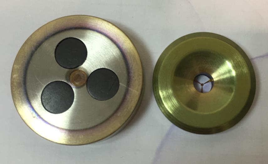
31 Targets on SCD and PECS Magnetron target (Au, Pt) demonstrating racetrack erosion profile PECS targets (Cr, Au/Pd, C and Pt)
32 Physical mechanisms of thin film growth (Video: Barna, 1967)
33
34 Thickness measurment Gravimetric method Measure substrate weight before and after coating Calculate thickness from known substrate dimensions Not real-time but surprisingly accurate Stylus method profilometer or AFM A stylus is drawn across a step in the film Scratching can occur Needs calibration Can do repeated measurements Not real-time (Image: wiki) (Image: l-w)


35 Thickness measurment Quartz crystal monitors - Quartz oscillator Specific oscillation frequency Expose one side of wafer to the vapor As the vapor coats the wafer the oscillation frequency changes Different parameters, proper calibration, quartz quality and proper usage If 6MHz oscillator is used nanogram changes can be measured in turn that means to 0,1A (Image: lesker)
36 What material should I coat with? Au: standard for sputtering, easy to coat, inert, stable under electron beam Au/Pd: all the advantages of Au bus smaller grain size Pt: highly inert, very conductive but large grain size Cr: smallest grain size, but oxides quickly C: best for X-ray microanalysis and EBSD
37 Influence of the Coating Material to the Quality 0.4 nm nominal film thickness (magnetron sputter) coatings produced at room temperature at low vacuum conditions

38 TEM coating
39 Take home information Before SEM characterization Check recent published papers Preparation of bulk (soft and hard) material Think what you want to image (surface, fractures, ) and prepare the sample Preparation of powders Make sure that there are firmly attached Mounting: holders and adhesives Different holders (carbon, aluminum) Different adhesives, always wait for the adhesives to dry, check if it has to be heated Coating: sputtering and evaporation Always make ground Choose the coating depending on the imaging and sample, for BSE use carbon, for biological specimens use higher Z. Thin film growth Different ways how the film growths Be sure that the surface image is not the coating, use some uncoated sample to check


40 Slovene Society for Microscopy

41
SEM sample preparation
 SEM sample preparation 6 th CEMM workshop Maja Koblar, Sc. Eng. Physics Outline Before SEM characterization Preparation of: bulk material hard and soft powders Mounting: holders and adhesives Coating:
Platypus Gold Coated Substrates. Bringing Science to the Surface
 Platypus Gold Coated Substrates Bringing Science to the Surface Overview Gold Coated Substrates - Gold Coating Introduction - Glossary of Terms - Gold Coating Methods - Critical Features Platypus Gold
Previous Lecture. Vacuum & Plasma systems for. Dry etching
 Previous Lecture Vacuum & Plasma systems for Dry etching Lecture 9: Evaporation & sputtering Objectives From this evaporation lecture you will learn: Evaporator system layout & parts Vapor pressure Crucible
Thin Films: Sputtering Systems (Jaeger Ch 6 & Ruska Ch 7,) Can deposit any material on any substrate (in principal) Start with pumping down to high
 Can deposit any material on any substrate (in principal) Start with pumping down to high") Thin Films: Sputtering Systems (Jaeger Ch 6 & Ruska Ch 7,) Can deposit any material on any substrate (in principal) Start with pumping down to high vacuum ~10-7 torr Removes residual gases eg oxygen from
Thin Films: Sputtering Systems (Jaeger Ch 6 & Ruska Ch 7,) Can deposit any material on any substrate (in principal) Start with pumping down to high vacuum ~10-7 torr Removes residual gases eg oxygen from
AP 5301/8301 LABORATORY MANUAL
 AP 5301/8301 LABORATORY MANUAL Department of Physics & Materials Science City University of Hong Kong Contents Table of Contents. 1 Project 1: Scanning Electron Microscopy (SEM). 2 Project 2: Microscopic
Image Formation and Interpretation
 Image Formation and Interpretation SEM Imaging Process Electron gun generates high energy electrons which are focused into a fine beam, which is scanned across the surface of the specimen. Elastically
Description. Spectro Tabs, higher purity conductive carbon tabs,12mm O.D.
 Description SPEC The simplicity of application and smooth, clean surfaces of PELCO Tabs Carbon Conductive Tabs are a significant improvement compared to many of the other common adhesives that have been
Cleaning samples. Options available. » Do not use organic. » Never, never, use squeeze. » Use detergents instead e.g. » Carbon Dioxide snow
 Sample Preparation Cleaning samples» Do not use organic solvents as these are always contaminated, even when fresh electronic grade» Never, never, use squeeze or spray bottles» Use detergents instead e.g.
Thin Films: Sputtering Systems (Jaeger Ch 6 & Ruska Ch 7,) Sputtering: gas plasma transfers atoms from target to substrate Can deposit any material
 Sputtering: gas plasma transfers atoms from target to substrate Can deposit any material") Thin Films: Sputtering Systems (Jaeger Ch 6 & Ruska Ch 7,) Sputtering: gas plasma transfers atoms from target to substrate Can deposit any material on any substrate (in principal) Start with pumping down
Thin Films: Sputtering Systems (Jaeger Ch 6 & Ruska Ch 7,) Sputtering: gas plasma transfers atoms from target to substrate Can deposit any material on any substrate (in principal) Start with pumping down
Thermal Evaporation. Theory
 Thermal Evaporation Theory 1. Introduction Procedures for depositing films are a very important set of processes since all of the layers above the surface of the wafer must be deposited. We can classify
GUIDELINE SAMPLE PREPARATION.
 Chapter 7 GUIDELINE SAMPLE PREPARATION. Samples come in all types, shapes and sizes, techniques therefore have to be found to cope with all variations and deviations from the perfect sample, a naturally
Metallization deposition and etching. Material mainly taken from Campbell, UCCS
 Metallization deposition and etching Material mainly taken from Campbell, UCCS Application Metallization is back-end processing Metals used are aluminum and copper Mainly involves deposition and etching,
Fabrication Process. Crystal Growth Doping Deposition Patterning Lithography Oxidation Ion Implementation CONCORDIA VLSI DESIGN LAB
 Fabrication Process Crystal Growth Doping Deposition Patterning Lithography Oxidation Ion Implementation 1 Fabrication- CMOS Process Starting Material Preparation 1. Produce Metallurgical Grade Silicon
Transmission Electron Microscopy (TEM) Prof.Dr.Figen KAYA
 Prof.Dr.Figen KAYA") Transmission Electron Microscopy (TEM) Prof.Dr.Figen KAYA Transmission Electron Microscope A transmission electron microscope, similar to a transmission light microscope, has the following components along
Transmission Electron Microscopy (TEM) Prof.Dr.Figen KAYA Transmission Electron Microscope A transmission electron microscope, similar to a transmission light microscope, has the following components along
Specimen configuration
 APPLICATIONNOTE Model 1040 NanoMill TEM specimen preparation system Specimen configuration Preparing focused ion beam (FIB) milled specimens for submission to Fischione Instruments. The Model 1040 NanoMill
Specimen Preparation Technique for a Microstructure Analysis Using the Focused Ion Beam Process
 Specimen Preparation Technique for a Microstructure Analysis Using the Focused Ion Beam Process by Kozue Yabusaki * and Hirokazu Sasaki * In recent years the FIB technique has been widely used for specimen
Coatings. Ion Assisted Deposition (IAD) process Advance Plasma Source (APS) plasma-ion assisted Deposition. Coatings on Optical Fibers
 process Advance Plasma Source (APS) plasma-ion assisted Deposition. Coatings on Optical Fibers") Anti-Reflection Custom Ion Assisted Deposition (IAD) process Advance Plasma Source (APS) plasma-ion assisted Deposition Anti-Reflection on Optical Fibers OptoSigma supplies a wide selection of optical
Anti-Reflection Custom Ion Assisted Deposition (IAD) process Advance Plasma Source (APS) plasma-ion assisted Deposition Anti-Reflection on Optical Fibers OptoSigma supplies a wide selection of optical
Chapter 3 Silicon Device Fabrication Technology
 Chapter 3 Silicon Device Fabrication Technology Over 10 15 transistors (or 100,000 for every person in the world) are manufactured every year. VLSI (Very Large Scale Integration) ULSI (Ultra Large Scale
Intlvac Nanochrome I Sputter System (intlvac_sputter)
") 1. Intlvac_Sputter Specifications The Intlvac Nanochrome I sputter system is configured for DC, AC (40 khz), and RF (13.56 MHz) magnetron sputtering. They system has in-situ quartz lamp heating up to 200C,
1. Intlvac_Sputter Specifications The Intlvac Nanochrome I sputter system is configured for DC, AC (40 khz), and RF (13.56 MHz) magnetron sputtering. They system has in-situ quartz lamp heating up to 200C,
A STUDY OF THE EFFECTIVENESS OF THE REMOVAL OF HYDROCARBON CONTAMINATION BY OXIDATIVE CLEANING INSIDE THE SEM.
 A STUDY OF THE EFFECTIVENESS OF THE REMOVAL OF HYDROCARBON CONTAMINATION BY OXIDATIVE CLEANING INSIDE THE SEM. Neal Sullivan, Tung Mai, Scott Bowdoin* and Ronald Vane** A poster paper presented at Microscopy
III Fabrication of the samples
 III Fabrication of the samples The fabrication of the samples for SPR measurement consists of three steps. It begins with glass substrates cleaning using ultrasonication, followed by the deposition of
Q150R Series Rotary Pumped Coaters
 Q u o r u m Te c h n ologies Q150R Modular Coating Systems Q Series Rotary Pumped Coating Systems Innovative and versatile sputter High vacuum sputtering and carbon coater and carbonfor evaporator evaporation
MODEL SEM Mill. Two independently adjustable TrueFocus ion sources
 MODEL 1060 SEM Mill A state-of-the-art ion milling and polishing system. It is compact, precise, and consistently produces high-quality scanning electron microscopy (SEM) samples for a wide variety of
IBS/e Ion Beam Sputter Deposition and Etching System. IBS/e with KDC-10 Ion Beam Sputter Deposition and Etching System with Kaufman Ion Source
 IBS/e Ion Beam Sputter Deposition and Etching System IBS/e with KDC-10 Ion Beam Sputter Deposition and Etching System with Kaufman Ion Source The Model IBS/e is a high vacuum thin film deposition system
The Physical Structure (NMOS)
") The Physical Structure (NMOS) Al SiO2 Field Oxide Gate oxide S n+ Polysilicon Gate Al SiO2 SiO2 D n+ L channel P Substrate Field Oxide contact Metal (S) n+ (G) L W n+ (D) Poly 1 3D Perspective 2 3 Fabrication
The Physical Structure (NMOS) Al SiO2 Field Oxide Gate oxide S n+ Polysilicon Gate Al SiO2 SiO2 D n+ L channel P Substrate Field Oxide contact Metal (S) n+ (G) L W n+ (D) Poly 1 3D Perspective 2 3 Fabrication
Advanced Manufacturing Choices
 Advanced Manufacturing Choices Table of Content Mechanical Removing Techniques Ultrasonic Machining (USM) Sputtering and Focused Ion Beam Milling (FIB) Ultrasonic Machining In ultrasonic machining (USM),
SUPPLEMENTARY INFORMATIONS
 SUPPLEMENTARY INFORMATIONS Dynamic Evolution of Conducting Nanofilament in Resistive Switching Memories Jui-Yuan Chen, Cheng-Lun Hsin,,, Chun-Wei Huang, Chung-Hua Chiu, Yu-Ting Huang, Su-Jien Lin, Wen-Wei
METHOD FOR IMPROVING FIB PREPARED TEM SAMPLES BY VERY LOW ENERGY Ar + ION MILL POLISHING
 METHOD FOR IMPROVING FIB PREPARED TEM SAMPLES BY VERY LOW ENERGY Ar + ION MILL POLISHING Yaron Kauffmann, Tzipi Cohen-Hyams, Michael Kalina, Hila Sadan-Meltzman and Wayne D. Kaplan Dept. of Materials Engineering
ITO. Crystal structure: Cubic, space group Ia3 No. 206, ci80, a = nm, Z = 16
 ITO Indium tin oxide (ITO) is a ternary composition of indium, tin and oxygen in varying proportions. Depending on the oxygen content, it can either be described as a ceramic or alloy. Indium tin oxide
CHEMICAL DEPTH PROFILING OF TOOL MATERIALS USING GLOW DISCHARGE OPTICAL EMISSION SPECTROSCOPY (GD-OES)
") CHEMICAL DEPTH PROFILING OF TOOL MATERIALS USING GLOW DISCHARGE OPTICAL EMISSION SPECTROSCOPY (GD-OES) T. Björk Swedish Institute for Metals Researc Drottning Kristinas väg 48 114 28 Stockholm Sweden Abstract
CHEMICAL DEPTH PROFILING OF TOOL MATERIALS USING GLOW DISCHARGE OPTICAL EMISSION SPECTROSCOPY (GD-OES) T. Björk Swedish Institute for Metals Researc Drottning Kristinas väg 48 114 28 Stockholm Sweden Abstract
Lecture Day 2 Deposition
 Deposition Lecture Day 2 Deposition PVD - Physical Vapor Deposition E-beam Evaporation Thermal Evaporation (wire feed vs boat) Sputtering CVD - Chemical Vapor Deposition PECVD LPCVD MVD ALD MBE Plating
The growth of patterned ceramic thin films from polymer precursor solutions Göbel, Ole
 University of Groningen The growth of patterned ceramic thin films from polymer precursor solutions Göbel, Ole IMPORTANT NOTE: You are advised to consult the publisher's version (publisher's PDF) if you
Study of Ion Beam Sputtering using Different Materials
 ab Journal of Nuclear Science and Applications, 5(), Study of Ion Beam Sputtering using Different Materials H. El-Khabeary Accelerators & Ion Sources Department, Basic Nuclear Science Division, Nuclear
I. PHYSICAL ELECTRONICS. Prof. W. B. Nottingham L. E. Sprague C. J. Marcinkowski R. Steinberg W. E. Mutter M. Wilkinson A. ELECTRON-EMISSION PROBLEMS
 I. PHYSICAL ELECTRONICS Prof. W. B. Nottingham L. E. Sprague C. J. Marcinkowski R. Steinberg W. E. Mutter M. Wilkinson A. ELECTRON-EMISSION PROBLEMS 1. Work Functions and Electrical Conductivity of Oxide-Coated
General Introduction to Microstructure Technology p. 1 What is Microstructure Technology? p. 1 From Microstructure Technology to Microsystems
 General Introduction to Microstructure Technology p. 1 What is Microstructure Technology? p. 1 From Microstructure Technology to Microsystems Technology p. 9 The Parallels to Microelectronics p. 15 The
Observation in the GB (Gentle Beam) Capabilities
 Capabilities") A field-emission cathode in the electron gun of a scanning electron microscope provides narrower probing beams at low as well as high electron energy, resulting in both improved spatial resolution and
A field-emission cathode in the electron gun of a scanning electron microscope provides narrower probing beams at low as well as high electron energy, resulting in both improved spatial resolution and
Growth Of TiO 2 Films By RF Magnetron Sputtering Studies On The Structural And Optical Properties
 Journal of Multidisciplinary Engineering Science and Technology (JMEST) Growth Of TiO 2 Films By RF Magnetron Sputtering Studies On The Structural And Optical Properties Ahmed K. Abbas 1, Mohammed K. Khalaf
Transmission Kikuchi Diffraction in the Scanning Electron Microscope
 Transmission Kikuchi Diffraction in the Scanning Electron Microscope Robert Keller, Roy Geiss, Katherine Rice National Institute of Standards and Technology Nanoscale Reliability Group Boulder, Colorado
Effect of substrate heating on elimination of pinholes in sputtering deposited SiO2 films on LiNbO3 single crystal substrates
 Thin Solid Films 335 (1998) 117-121 Effect of substrate heating on elimination of pinholes in sputtering deposited SiO2 films on LiNbO3 single crystal substrates Hirotoshi Nagata a, *, Tetsuya Fujino b,
EE 5344 Introduction to MEMS. CHAPTER 3 Conventional Si Processing
 3. Conventional licon Processing Micromachining, Microfabrication. EE 5344 Introduction to MEMS CHAPTER 3 Conventional Processing Why silicon? Abundant, cheap, easy to process. licon planar Integrated
Supporting Information for Surface-energy induced formation of single crystalline. bismuth nanowires over vanadium thin film at room temperature
 Supporting Information for Surface-energy induced formation of single crystalline bismuth nanowires over vanadium thin film at room temperature Mingzhao Liu,* 1 Jing Tao, 2 Chang-Yong Nam, 1 Kim Kisslinger,
Supporting Information
 Supporting Information Novel Sample Preparation Technique to Improve Spectromicroscopic Analyses of Micrometer- Sized Particles Carmen Höschen *, Till Höschen, Carsten W. Mueller, Johann Lugmeier, Stefan
Ion-plasma technologies and equipment
 Ion-plasma technologies and equipment VACUUM ION-PLASMA INSTALLATIONS OF «OPAL» SERIES «Opal» series ion-plasma installations are designed for deposition of low-emission, reflective and toned coatings
CHAPTER 4. SYNTHESIS OF ALUMINIUM SELENIDE (Al 2 Se 3 ) NANO PARTICLES, DEPOSITION AND CHARACTERIZATION
 NANO PARTICLES, DEPOSITION AND CHARACTERIZATION") 40 CHAPTER 4 SYNTHESIS OF ALUMINIUM SELENIDE (Al 2 Se 3 ) NANO PARTICLES, DEPOSITION AND CHARACTERIZATION 4.1 INTRODUCTION Aluminium selenide is the chemical compound Al 2 Se 3 and has been used as a precursor
40 CHAPTER 4 SYNTHESIS OF ALUMINIUM SELENIDE (Al 2 Se 3 ) NANO PARTICLES, DEPOSITION AND CHARACTERIZATION 4.1 INTRODUCTION Aluminium selenide is the chemical compound Al 2 Se 3 and has been used as a precursor
Linear Plasma Sources for Surface Modification and Deposition for Large Area Coating
 Linear Plasma Sources for Surface Modification and Deposition for Large Area Coating Dr Tony Williams Gencoa Ltd, UK Victor Bellido-Gonzalez, Dr Dermot Monaghan, Dr Joseph Brindley, Robert Brown SVC 2016,
Transzmissziós és pásztázó elektronmikroszkópos minták készítése ionsugaras vékonyítással
 Transzmissziós és pásztázó elektronmikroszkópos minták készítése ionsugaras vékonyítással Radi Zsolt Technoorg Linda Kft., Budapest Oktatói és Doktorandusz Konferencia Visegrád, 2012 State-of-the-art materials
Transactions on Engineering Sciences vol 2, 1993 WIT Press, ISSN
 A study of thin-film continuous coating process by vapour deposition P. Gimondo," F. Arezzo,* B. Grifoni,* G. Jasch& "Centra Sviluppo Materiali SpA, Via di Castel & Von Ardenne Anlagentchnik GmbH, Plattleite
Sputter Coating. Technical Brief
 Sputter Coating Technical Brief Document Number TB-SPUTTER Issue 2 (01/02) Introduction HP000107 Quorum Technologies Ltd main sales office: South Stour Avenue Ashford Kent U.K. Tel: ++44(0) 1233 646332
Microtexture measurement of copper damascene line with EBSD
 Material Science Forum Vols. 408-412(2002) pp. 529-534 2002 Trans Tech Publications, Switzerland Microtexture measurement of copper damascene line with EBSD Dong-Ik Kim 1*, Jong-Min Paik 1, Young-Chang
Introduction to Electron Microscopy Andres Kaech
 Center for Microscopy and Image Analysis Introduction to Electron Microscopy Andres Kaech The types of electron microscopes Transmission electron microscope (TEM) Scanning electron microscope (SEM) 1 The
Fabrication Technology
 Fabrication Technology By B.G.Balagangadhar Department of Electronics and Communication Ghousia College of Engineering, Ramanagaram 1 OUTLINE Introduction Why Silicon The purity of Silicon Czochralski
Supplementary Materials for
 www.sciencemag.org/cgi/content/full/336/6084/1007/dc1 Supplementary Materials for Unidirectional Growth of Microbumps on (111)-Oriented and Nanotwinned Copper Hsiang-Yao Hsiao, Chien-Min Liu, Han-wen Lin,
Growth of monocrystalline In 2 O 3 nanowires by seed orientation dependent vapour-solid-solid mechanism
 Electronic Supplementary Material (ESI) for Journal of Materials Chemistry C. This journal is The Royal Society of Chemistry 2014 Electronic Supplementary Information (ESI) Growth of monocrystalline In
EVALUATION OF ADHESION, HARDNESS AND MICROSTRUCTURE OF CrN e CrAlN COATINGS DEPOSITED BY HIGH POWER IMPULSE MAGNETRON SPUTTERING
 EVALUATION OF ADHESION, HARDNESS AND MICROSTRUCTURE OF e CrAlN COATINGS DEPOSITED BY HIGH POWER IMPULSE MAGNETRON SPUTTERING Bruno César Noronha Marques de Castilho, Mechanical Engineering - Materials,
Carnegie Mellon MRSEC
 Carnegie Mellon MRSEC Texture, Microstructure & Anisotropy, Fall 2009 A.D. Rollett, P. Kalu 1 ELECTRONS SEM-based TEM-based Koseel ECP EBSD SADP Kikuchi Different types of microtexture techniques for obtaining
Polymer Microscopy. Second edition LINDA C. SAWYER. and. DAVID T. GRUBB Cornell University Ithaca, NY USA. Hoechst Celanese Corporation Summit, NJ USA
 Polymer Microscopy Second edition LINDA C. SAWYER Hoechst Celanese Corporation Summit, NJ USA and DAVID T. GRUBB Cornell University Ithaca, NY USA CHAPMAN & HALL London Glasgow Weinheim New York Tokyo
The principles and practice of electron microscopy
 The principles and practice of electron microscopy Second Edition Ian M. Watt CAMBRIDGE UNIVERSITY PRESS Contents Preface tofirstedition page ix Preface to second edition xi 1 Microscopy with light and
Formation mechanism of new corrosion resistance magnesium thin films by PVD method
 Surface and Coatings Technology 169 170 (2003) 670 674 Formation mechanism of new corrosion resistance magnesium thin films by PVD method a, a a a b M.H. Lee *, I.Y. Bae, K.J. Kim, K.M. Moon, T. Oki a
JSM-7800F Field Emission Scanning Electron Microscope
 JSM-7800F catalogue JSM-7800F Field Emission Scanning Electron Microscope We provide high performance The Ultimate Research Tool for Multi-Disciplinary Research Institutions Extreme resolution The super
From Eye to Insight. Leica EM ACE. Coater Family
 From Eye to Insight Leica EM ACE Coater Family EM ACE COATERS A Coater Family to cover all your needs. Developed in cooperation with leading scientists, the EM ACE coaters cover all the requirements for
SUPPLEMENTARY INFORMATION
 High Electrochemical Activity of the Oxide Phase in Model Ceria- and Ceria-Ni Composite Anodes William C. Chueh 1,, Yong Hao, WooChul Jung, Sossina M. Haile Materials Science, California Institute of Technology,
SPECIMEN PREPARATION FOR ELECTRON MICROSCOPY
 SPECIMEN PREPARATION FOR ELECTRON MICROSCOPY Samar Das Scientist National Metallurgical Laboratory Jamshedpur - 831 007 The purpose of electron microscopy is to study accurately the microstructures at
EBSD Basics EBSD. Marco Cantoni 021/ Centre Interdisciplinaire de Microscopie Electronique CIME. Phosphor Screen. Pole piece.
 EBSD Marco Cantoni 021/693.48.16 Centre Interdisciplinaire de Microscopie Electronique CIME EBSD Basics Quantitative, general microstructural characterization in the SEM Orientation measurements, phase
BAF 060 Freeze-Fracture System
 BAL-TEC AG EM-TECHNOLOGY AND APPLICATION BAF 060 GRE BAF 060 Freeze-Fracture System 20.05.99 Internet: www.bal-tec.com 1 / 6 BAF 060 - Designed to meet your needs Load-Lock Transfer of Specimen: For fast
Quantitative X-ray Microanalysis Of Submicron Carbide Formation In Chromium (III) Oxide Rich Scale
 Oxide Rich Scale") Quantitative X-ray Microanalysis Of Submicron Carbide Formation In Chromium (III) Oxide Rich Scale W. Keith Collins*, M. Ziomek-Moroz, G. R. Holcomb, P. Danielson, and A. Hunt *National Energy Technology
Quantitative X-ray Microanalysis Of Submicron Carbide Formation In Chromium (III) Oxide Rich Scale W. Keith Collins*, M. Ziomek-Moroz, G. R. Holcomb, P. Danielson, and A. Hunt *National Energy Technology
Czochralski Crystal Growth
 Czochralski Crystal Growth Crystal Pulling Crystal Ingots Shaping and Polishing 300 mm wafer 1 2 Advantage of larger diameter wafers Wafer area larger Chip area larger 3 4 Large-Diameter Wafer Handling
Manufacturing Technologies for MEMS and SMART SENSORS
 4 Manufacturing Technologies for MEMS and SMART SENSORS Dr. H. K. Verma Distinguished Professor (EEE) Sharda University, Greater Noida (Formerly: Deputy Director and Professor of Instrumentation Indian
Surface Layer Characterization of Atomized Magnesium for use in Powder Metallurgy Products Paul Burke and Georges J. Kipouros
 Surface Layer Characterization of Atomized Magnesium for use in Powder Metallurgy Products Paul Burke and Georges J. Kipouros Materials Engineering Program Process Engineering and Applied Science Dalhousie
MODEL 1051 TEM Mill ION MILLING. Ion milling is used on physical science. specimens to reduce thickness to electron
 MODEL 1051 TEM Mill A state-of-the-art ion milling and polishing system offering reliable, high performance specimen preparation. It is compact, precise, and consistently produces high-quality transmission
Surface Micromachining
 Surface Micromachining Micro Actuators, Sensors, Systems Group University of Illinois at Urbana-Champaign Outline Definition of surface micromachining Most common surface micromachining materials - polysilicon
Chemical Vapour Deposition: CVD Reference: Jaeger Chapter 6 & Ruska: Chapter 8 CVD - Chemical Vapour Deposition React chemicals to create a thin film
 Chemical Vapour Deposition: CVD Reference: Jaeger Chapter 6 & Ruska: Chapter 8 CVD - Chemical Vapour Deposition React chemicals to create a thin film layer at the surface Typically gas phase reactions
Good Practice Guide for nanoindentation of nanoparticles embedded in a layer using an SEM in situ technique
 Sample preparation The particles to be tested were two sizes of silica spherical particles, nominally sized 300 nm and 100 nm in diameter, gold spherical particles, nominally sized 60 nm in diameter, and
Lab #2 Wafer Cleaning (RCA cleaning)
") Lab #2 Wafer Cleaning (RCA cleaning) RCA Cleaning System Used: Wet Bench 1, Bay1, Nanofabrication Center Chemicals Used: H 2 O : NH 4 OH : H 2 O 2 (5 : 1 : 1) H 2 O : HF (10 : 1) H 2 O : HCl : H 2 O 2
Lab #2 Wafer Cleaning (RCA cleaning) RCA Cleaning System Used: Wet Bench 1, Bay1, Nanofabrication Center Chemicals Used: H 2 O : NH 4 OH : H 2 O 2 (5 : 1 : 1) H 2 O : HF (10 : 1) H 2 O : HCl : H 2 O 2
ECE 440 Lecture 27 : Equilibrium P-N Junctions I Class Outline:
 ECE 440 Lecture 27 : Equilibrium P-N Junctions I Class Outline: Fabrication of p-n junctions Contact Potential Things you should know when you leave Key Questions What are the necessary steps to fabricate
By *T.Khalil, **J. Bossert,***A.H.Ashor and *F. Abou EL-Nour
 WM 11 EG0100132 Seventh Conference of Nuclear Sciences & Applications 6-10 February 2000. Cairo, Egypt Preparation, Characterization and application of Alumina powder Produced by advanced Preparation Techniques
Silver Diffusion Bonding and Layer Transfer of Lithium Niobate to Silicon
 Chapter 5 Silver Diffusion Bonding and Layer Transfer of Lithium Niobate to Silicon 5.1 Introduction In this chapter, we discuss a method of metallic bonding between two deposited silver layers. A diffusion
Nucleation and growth of nanostructures and films. Seongshik (Sean) Oh
 Oh") Nucleation and growth of nanostructures and films Seongshik (Sean) Oh Outline Introduction and Overview 1. Thermodynamics and Kinetics of thin film growth 2. Defects in films 3. Amorphous, Polycrystalline
Nucleation and growth of nanostructures and films Seongshik (Sean) Oh Outline Introduction and Overview 1. Thermodynamics and Kinetics of thin film growth 2. Defects in films 3. Amorphous, Polycrystalline
ECE 541/ME 541 Microelectronic Fabrication Techniques
 ECE 541/ME 541 Microelectronic Fabrication Techniques MW 4:00-5:15 pm Introduction to Vacuum Technology Zheng Yang ERF 3017, email: yangzhen@uic.edu ECE541/ME541 Microelectronic Fabrication Techniques
EECS130 Integrated Circuit Devices
 EECS130 Integrated Circuit Devices Professor Ali Javey 9/13/2007 Fabrication Technology Lecture 1 Silicon Device Fabrication Technology Over 10 15 transistors (or 100,000 for every person in the world)
Biomimetic synthesis of gold nanocrystals using a reducing amphiphile. Ferdinand Gonzaga, Sherdeep Singh and Michael A. Brook. Department of Chemistry
 Biomimetic synthesis of gold nanocrystals using a reducing amphiphile. Ferdinand Gonzaga, Sherdeep Singh and Michael A. Brook Department of Chemistry 1280 Main St. W. Hamilton ON L8S 4M1 Canada Outline
All fabrication was performed on Si wafers with 285 nm of thermally grown oxide to
 Supporting Information: Substrate preparation and SLG growth: All fabrication was performed on Si wafers with 285 nm of thermally grown oxide to aid in visual inspection of the graphene samples. Prior
XTEM characterization of modulated ion implantation through self-organized anodic aluminium oxide (AAO) membranes
 membranes") XTEM characterization of modulated ion implantation through self-organized anodic aluminium oxide (AAO) membranes Wei Guan 1, Jay Ghatak 1, Nianhua Peng 2, Yong Peng 1, Chris Jeynes 2, Beverley Inkson
XTEM characterization of modulated ion implantation through self-organized anodic aluminium oxide (AAO) membranes Wei Guan 1, Jay Ghatak 1, Nianhua Peng 2, Yong Peng 1, Chris Jeynes 2, Beverley Inkson
Morphological Investigations - Different Microscopic Techniques (Semicrystalline Polymers)
") Morphological Investigations - Different Microscopic Techniques (Semicrystalline Polymers) Method SEM TEM AFM Typical Sample Preparation Evaporation Surface Etching Ultramicrotomy Selective Staining no
Morphological Investigations - Different Microscopic Techniques (Semicrystalline Polymers) Method SEM TEM AFM Typical Sample Preparation Evaporation Surface Etching Ultramicrotomy Selective Staining no
The Study of SEM Examination of Crept Ceramic Samples Prepared by Cross Polishing Method
 The Study of SEM Examination of Crept Ceramic Samples Prepared by Cross Polishing Method Alper Uludag Faculty of Aeronautics and Astronautics Anadolu University Eskisehir, Turkey alperuludag@anadolu.edu.tr
Microstructure, morphology and their annealing behaviors of alumina films synthesized by ion beam assisted deposition
 Nuclear Instruments and Methods in Physics Research B 206 (2003) 357 361 www.elsevier.com/locate/nimb Microstructure, morphology and their annealing behaviors of alumina films synthesized by ion beam assisted
Thin Film Gas Sensor. Nanoelectronics and MEMS Laboratory National Electronics and Computer Technology
 Ion-assisted E-beam E Evaporated Thin Film Gas Sensor A. Wisitsoraat,, A. A Tuantranont,, V. V Patthanasettakul, T. Lomas,, and P. Chindaudom Nanoelectronics and MEMS Laboratory National Electronics and
"Thin Film Technology" "Physics of Thin Films"
 D r d "Thin Film Technology" "Physics of Thin Films" Contents: Preface 1. Introduction 1.1. General 1.2. History 1.3. Definition of Terms 1.4. Applications of Thin Film Technology 1.5. Deposition Methods
Embedded Passives..con0nued
 Embedded Passives..con0nued Why Embedded Passives? Improves the packaging efficiency System-on-Package (SOP); SLIM integration Reducing size Eliminating substrate assembly Minimizing solder joint failure
Simple method for formation of nanometer scale holes in membranes. E. O. Lawrence Berkeley National Laboratory, Berkeley, CA 94720
 Simple method for formation of nanometer scale holes in membranes T. Schenkel 1, E. A. Stach, V. Radmilovic, S.-J. Park, and A. Persaud E. O. Lawrence Berkeley National Laboratory, Berkeley, CA 94720 When
Evaluation Methods of Concrete Carbonation Suppressive Performance of Surface Coating
 Evaluation Methods of Concrete Carbonation Suppressive Performance of Surface Coating Kenji Motohashi Shibaura Institute of Technology, Japan Toyosu 3-7-, Koto-Ku, 13-848 Japan, motoken@shibaura-it.ac.jp
X-ray Photoelectron Spectroscopy
 X-ray Photoelectron Spectroscopy X-ray photoelectron spectroscopy (XPS) is a non-destructive technique used to analyze the elemental compositions, chemical and electronic states of materials. XPS has a
Studentská 1402/ Liberec 1 tel.: cxi.tul.cz. Technology equipment
 Technology equipment Department of prototype technologies and processes 3D Printer Objet Connex 500 3D print technology PolyJet Matrix System Objet modelling from ABS-like material for larger and accurate
Chapter 3: Powders Production and Characterization
 Chapter 3: Powders Production and Characterization Course Objective... To introduce selective powder production processes and characterization methods. This course will help you : To understand properties
2008 Summer School on Spin Transfer Torque
 2008 Summer School on Spin Transfer Torque Nano-scale device fabrication 2-July-2008 Byoung-Chul Min Center for Spintronics Research Korea Institute of Science and Technology Introduction Moore s Law
Alternatives to Aluminium Metallization
 Alternatives to Aluminium Metallization Technological pressures on the speed and reliability of integrated circuits has caused a need for changes to be made in the choices of materials used for metallization
Various Techniques for Reliability Estimation and Failure Analysis of Electronic Products and Components
 JFE No. 13 2006 8 p. 97 102 Various Techniques for Reliability Estimation and Failure Analysis of Electronic Products and Components BAN Mitsuyuki SHIMAUCHI Yutaka JFE JFE JFE X IC Pb Abstract: JFE Techno-Research
METHODS OF COATING FABRICATION
 METHODS OF COATING FABRICATION Zbigniew Grzesik http://home.agh.edu.pl/~grzesik Department of Physical Chemistry and Modelling DEFINITION The coating is the thin outer layer of the object, which physiochemical
The most important parameters determining the performance of a cutting blade are:
 Diamond blades exceptionally wear resistant and extremely sharp P. Gluche 1, S. Strobel 1, H.-J. Fecht 2 1 GFD Gesellschaft für Diamantprodukte mbh, Lise-Meitner-Str. 13, 89081 Ulm, Germany 2 University
EQUIPMENT AND SYSTEM FOR VACUUM COATING METALLIZING, SPUTTERING, PLASMA and PECVD. Hybrid system KOLZER DGK 36
 email : carlo.gennari@fastwebnet.it web site : http://carlogennariforni.beepworld.it/kolzer.htm EQUIPMENT AND SYSTEM FOR VACUUM COATING METALLIZING, SPUTTERING, PLASMA and PECVD Hybrid system KOLZER DGK
Electron Probe Micro-Analysis (EPMA)
") Electron Probe Micro-Analysis (EPMA) Nilanjan Chatterjee, Ph.D. Principal Research Scientist 1 Electron Microprobe Facility Department of Earth, Atmospheric and Planetary Sciences Massachusetts Institute
Electron Probe Micro-Analysis (EPMA) Nilanjan Chatterjee, Ph.D. Principal Research Scientist 1 Electron Microprobe Facility Department of Earth, Atmospheric and Planetary Sciences Massachusetts Institute