THIN FILM ANALYZER TFA
|
|
|
- Bryan Hart
- 6 years ago
- Views:
Transcription

1 T H E R M A L A N A L Y S I S THIN FILM ANALYZER TFA

2 Since 1957 LINSEIS Corporation has been delivering outstanding service, know how and leading innovative products in the field of thermal analysis and thermo physical properties. Customer satisfaction, innovation, flexibility and high quality are what LINSEIS represents. Thanks to these fundamentals our company enjoys an exceptional reputation among the leading scientific and industrial organizations. LINSEIS has been offering highly innovative benchmark products for many years. The LINSEIS business unit of thermal analysis is involved in the complete range of thermo analytical equipment for R&D as well as quality control. We support applications in sectors such as polymers, chemical industry, inorganic building materials and environmental analytics. In addition, thermo physical properties of solids, liquids and melts can be analyzed. Claus Linseis Managing Director LINSEIS provides technological leadership. We develop and manufacture thermo-analytic and thermo-physical testing equipment to the highest standards and precision. Due to our innovative drive and precision, we are a leading manufacturer of thermal Analysis equipment. The development of thermo analytical testing machines requires significant research and a high degree of precision. LINSEIS Corp. invests in this research to the benefit of our customers. We are driven by innovation and customer satisfaction. 2


3 German engineering The strive for the best due diligence and accountability is part of our DNA. Our history is affected by German engineering and strict quality control. Innovation We want to deliver the latest and best technology for our customers. LINSEIS continues to innovate and enhance our existing thermal analyzers. Our goal is constantly develop new technologies to enable continued discovery in Science. 3

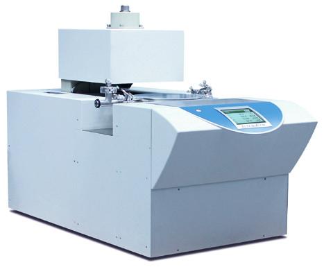
4 THIN FILM ANALYZER The LINSEIS Thin Film Analyzer is the perfect solution to characterize a broad range of thin film samples in a very comfortable and quick way. It is an easy to use, single stand alone system and delivers high quality results using an optimized measurement design as well as the proven LINSEIS Firmware and Software package. Motivation Due to new research efforts in the field of semiconducting materials with a focus on size effects, there is a growing need for measurement setups dedicated to samples with small geometrical dimensions like thin films and nanowires with considerably different physical properties than bulk material. The characterization of these samples is important to learn more about their structure and conduction mechanism but also important for technical applications. Measurement Setup The LINSEIS TFA is a chip-based platform to simultaneously measure the in-plane electrical and thermal conductivity, the Seebeck coefficient as well as the Hall constant of a thin film sample in the temperature range from -170 C up to 300 C and in a magnetic field of up to 1 T. Due to the design of the setup, time consuming preparation steps can be omitted and a nearly simultaneous measurement of the sample properties is achieved. Typical errors caused by different sample compositions, varying sample geometries and different heat profiles are avoided with this measurement method. The System can handle a broad range of different materials. It is possible to measure samples with semocinducting behaviour as well as metalls, ceramics or organics. Therefore many different deposition methods like PVD or Spin coating and drop casting are possible to use. 4

5 MEASURING SETUP Components The basic setup consists of a measurement chip on which the sample can be easily deposited, and the measurement chamber to provide the required environmental conditions. Depending on the application, the setup can be utilized with a Lock-In amplifier and / or a strong electric magnet. The measurements are usually taken under UHV and the samples temperature can be controlled between -170 C and +300 C during the measurement using LN 2 and powerful heaters. Modular design Starting with a basic setup to measure the thermal conductivity, the system can easily be upgraded with either the thermoelectric kit to measure the electrical conductivity and Seebeck coefficient or with the magnetic upgrade kit to take Hall constant, mobility and charge carrier concentration measurements. Measuring chamber 5
 Consists of measurement chamber, vacuum pump, basic sample holder with included heater, system integrated lock-in amplifier for the 3w-method, PC and LINSEIS Software packag")
 and evaluation software for thermoelectric experiments.")
6 PACKAGING OPTIONS Following packaging options are available for the LINSEIS Thin Film Analyzer (TFA): 1. Basic device (incl. transient package) Consists of measurement chamber, vacuum pump, basic sample holder with included heater, system integrated lock-in amplifier for the 3w-method, PC and LINSEIS Software packag including measurement and evaluation software. The design is optimized to measure following physical properties: l - Thermal Conductivity c p - Specific Heat e - Emissivity (depends on material) 2. Thermoelectric package Consisting of extended measurment electronics (DC) and evaluation software for thermoelectric experiments. The design is optimized for measuring the following parameters: s - Electrical Conductivity / Electrical Resistivity S - Seebeck Coefficient 3. Magnetic package The design is optimized for measuring the following parameters: A H - Hall Constant μ - Mobility n - Charge carrier concentration 4. Low temperature option for controlled cooling down to 100 K TFA/KREG controlled cooling unit TFA/KRYO Dewar 25l Software The TFA software package consists of two parts. A measurement software which displays the actual values as well as allows to define a measurement routine and the dircet control of the setup. And an additional evaluation software for the post processing of the measured raw data. Measurement software Evaluation software 6
7 MEASURING PRINCIPLES Pre structured measuring chips The chip is combining the 3 Omega measurement technique for the thermal conductivity measurement with a 4-point Van-der-Pauw setup for the determination of the electrical transport properties. The Seebeck coefficient can be measured using additional resistance thermometers located near the Van-der-Pauw electrodes. For an easy sample preparation either a strip off foil mask or a metal shadow mask can be used. This configuration allows for a nearly simultaneous characterization of a sample which has been prepared by either PVD (e.g. thermal evaporation, sputtering, MBE), CVD (e.g. ALD), spin coating, drop casting or ink-jet printing in one step. 1. Van-der-Pauw measurement To determine the electrical conductivity (s) and Hall coefficient (AH) of the sample, the Vander-Pauw method is used. After depositing the sample on the chip, it is already connected to four elec trodes A, B, C & D at their edge. For the measurement, a current is applied between two of the contacts and the corresponding voltage between the remaining two is measured. By clockwise changing of the contacts and repeating of the procedure, the resistivity of the sample can be calculated using the Van-der-Pauw equation. πd πd exp ( R AB,CD ) + exp ( R BC,DA ) r By applying a magnetic field and measuring the corresponding change of the diagonal Van-der- Pauw resistance, the Hall coefficient of the sample can be calculated. A H = d B R AC,BD For the determination of the Seebeck Coefficient, an additional thermometer and heater is placed on the chip near the sample. This configuration allows for the measurment of the thermovoltage at different temperature gradients wich can be used in order to calculate the Seebeck Coefficient S=-Vth/ T. S = V th / T r 7
8 2. Hot stripe measurement For the deterimation of the in-plane thermal conductivity, a patend pending hot-stripe suspended membrane setup is used. In this setup, a very small wire is used as heater and temperature sensor in one. The sample of interrest will be deposited directly on this membrane. For the measurment, a current is applied to the hotwire which is heated up due to Joule heating. Because of the temperature rise, the resistivity of the wire is changing and can be measured easily. From this resistivity change and the knowledge of the exact geomtrie of the setup, it is possible to calculate back to the thermal conductivity of the sample. Depending on the sample, it is also possible to measure the emis sivity and specific heat. In order to get high quality results, the sample thickness times sample thermal conductivity should be equal or bigger than 2 x 10⁻⁷ W/K. Membrane (λ M d M ) Pt rim Hot wire Pt rim Sample (λ S d S ) Passivation layer (λ P d P ) Silicon 8


9 Hall option TFA with Hall option (moveable electromagnet with up to 1 Tesla) 9
10 TECHNICAL SPECIFICATIONS General Temperature range RT up to 200 C -170 C up to 300 C Sample thickness Measurement principle Desposition techiques Measured parameters Optional Vacuum Electronics Interface from only a few nm to µm range (depends on sample) chip based (pre structured measurement chips, 24 pcs. per box) include: PVD (sputtering, evaporation), ALD, spin coating, ink-jet printing and more Thermal Conductivity (3 Omega) Specific Heat Seebeck Coefficient Electrical Resisitivity / Conductivity Hall Constant / Mobility / Charge carrier conc. permanent magnet 0.5 T or electromagnet up to 1 T up to 10-5 bar integrated USB Measurement range Thermal Conductivity Electrical Resistivity Seebeck Coefficient 0.05 up to 200 W/m K 0.05 up to S/cm 1 up to 2500 µv/k Repeatability & Accuracy Thermal Conductivity Electrical Resistivity Seebeck Coefficient ± 10% (for most materials) ± 6% (for most materials) ± 7% (for most materials) 10


11 APPLICATIONS Thermoelectric devices A typical application is the characterization of thin films made out of thermoelectric materials. A lot of research is done to improve the efficiency of thermoelectric devices. Integrated devices For the development and design of new and robust integrated devices like sensors or microchips, the semiconducting industry needs to know a lot about the physical properties of the used films. For example for the heat management or the electric insolation of such devices. Thermal barrier coatings Another interesting field for thin films are thermal barrier coatings as they are used in aircraft engines. Many new materials have been developed and characterized, especially in regard to their thermal behavior. Tribological stress The last application example is the determination of material parameters for thin films used in tools. The understanding is very important to avoid wear due to tribological stress to ensure an extended product life cycle. 11

12 APPLICATIONS Full ZT Characterization of a 142 nm Bi 87 Sb 13 thin film Measured electrical conductivity, thermal conductivity and Seebeck coefficient as well as calculated ZT value of a 142 nm thick Bi 87 Sb 13 nanofilm, prepared by thermal evaporation in the temperature range from 120 K up to 400 K. Thermal annealing effects observed at a Bi 87 Sb 13 thin film Thermal annealing effects observed at a 282 nm thin Bi 87 Sb 13 nanofilm prepared by thermal evaporation. After the first measurement run at elevated temperatures, the thermoelectric properties show strong thermal annealing effects caused by recristallisation and defect healing processes. 12

13 Full ZT Characterization of a PEDOT:PSS layer Measured electrical conductivity, thermal conductivity and Seebeck coefficient as well as calculated ZT value of a 15 µm thick PEDOT:PSS thin film, prepared by drop casting in the temperature range from 110 K up to 350 K. Full ZT Characterization of a Gold nanofilm Measured electrical conductivity, thermal conductivity and Seebeck coefficient as well as calculated ZT value of a 100 nm Au thin film, prepared by DC magnetron sputtering in the temperature range from 225 K up to 375 K. The results preflectly agree with the Wiedemann -Franz law and a clear influence of classical size effects has been observed. 13
14 LINSEIS GmbH Germany Vielitzerstr Selb Tel.: (+49) Fax: (+49) LINSEIS Inc. USA 109 North Gold Drive Robbinsville, NJ Tel.: (+1) Fax: (+1) LINSEIS China Kaige Scientific Park 2653 Hunan Road Shanghai Tel.: (+21) Fax.: (+21) LINSEIS France Bureaux Paris 52 Boulevard Sébastopol Paris Tel.: (+33) LINSEIS Poland ul. Dabrowskiego Pruszkow Tel.: (+48) Products: DIL, TG, STA, DSC, HDSC, DTA, TMA, MS/FTIR, In-Situ EGA, Laser Flash, Seebeck Effect, Thin Film Analyzer, Hall-Effect Services: Service Lab, Calibration Service 04/18
THIN FILM ANALYZER TFA
 T H E R M A L A N A L Y S I S THIN FILM ANALYZER TFA Since 1957 LINSEIS Corporation has been delivering outstanding service, know how and leading innovative products in the field of thermal analysis and
TFA Thin Film Analyzer
 TFA Thin Film Analyzer Thin Film Analyzer The LINSEIS Thin Film Analyzer is the perfect solution to characterize a broad range of thin film samples in a very comfortable and quick way. It is an easy to
HFM Heat Flow Meter Thermal Conductivity Analyzer
 HFM Heat Flow Meter Thermal Conductivity Analyzer Introduction An insulating material is a material with low thermal conductivity, which in the construction industry, equipment manufacturing, or the production
DIFFERENTIAL SCANNING CALORIMETER. Chip-DSC 100 Chip-DSC 10
 T H E R M A L A N A L Y S I S DIFFERENTIAL SCANNING CALORIMETER Chip-DSC 100 Chip-DSC 10 Since 1957 LINSEIS Corporation has been delivering outstanding service, know how and leading innovative products
Dilatometer L 76 L 75 Horizontal L 75 Vertical
 Dilatometer L 76 L 75 Horizontal L 75 Vertical General Dilatometry is a technique which measures the dimensional change of a substance as a function of temperature while the substance is subjected to a
THERMAL DIFFUSIVITY THERMAL CONDUCTIVITY
 THERMAL DIFFUSIVITY THERMAL CONDUCTIVITY Thermal Diffusivity, Thermal Conductivity Information of the thermo physical properties of materials and heat transfer optimization of final products is becoming
DILATOMETER Special Software
 DILATOMETER Special Software Software for Dilatometers Softening Point Software for Dilatometers All dilatometer delivered since 01. 11. 2002 has a new feature included in the WIN-DIL software. Softening
THERMO- GRAVIMETRIC ANALYZER TGA 1600
 T H E R M A L A N A L Y S I S THERMO- GRAVIMETRIC ANALYZER TGA 1600 Since 1957 LINSEIS Corporation has been delivering outstanding service, know how and leading innovative products in the field of thermal
Thermal Analysis & Thermo Physical Properties
 Thermal Analysis & Thermo Physical Properties Introduction... 3 DSC Differential Scanning Calorimeter... 4 HDSC / DTA High Temperature DSC/DTA... 6 TGA Thermal Gravimetric Analysis... 8 STA Simultaneous
A NOVEL METHOD FOR THE IMPROVEMENT IN THERMOELECTRIC PROPERTY OF TIN OXIDE THIN FILMS AND ITS APPLICATION IN GAS SENSING
 INTERNATIONAL JOURNAL ON SMART SENSING AND INTELLIGENT SYSTEMS, VOL. 1, NO. 2, JUNE 2008 A NOVEL METHOD FOR THE IMPROVEMENT IN THERMOELECTRIC PROPERTY OF TIN OXIDE THIN FILMS AND ITS APPLICATION IN GAS
THERMAL ANALYSIS & THERMO-PHYSICAL PROPERTIES
 THERMAL ANALYSIS & THERMO-PHYSICAL PROPERTIES Introduction 3 DSC Differential Scanning Calorimeter 4 STA Simultaneous Thermal Analysis 6 HDSC / DTA High Temperature DSC/DTA 12 DIL Dilatometry 14 TMA Thermomechanical
Productivity versus Profitability in Vacuum Web Coating
 Productivity versus Profitability in Vacuum Web Coating Liz Josephson, Applied Films Corp., Longmont, USA Dirk Hoffmann, Applied Films GmbH & Co KG, Alzenau, Germany Gerard Loebig, Applied Films GmbH &
THE DEVELOPMENT OF THE MICRO-GENERATOR ON THE SUBSTRATE BASED THIN FILM
 Proceedings of MNHT2008 Micro/Nanoscale Heat Transfer International Conference January 6-9, 2008, Tainan, Taiwan MNHT2008-52198 THE DEVELOPMENT OF THE MICRO-GENERATOR ON THE SUBSTRATE BASED THIN FILM Jun-ichiro
Analyzing & Testing. Guarded Hot Plate - GHP. Method, Instrumentation, Applications. GHP 456 Titan. Leading Thermal Analysis
 Analyzing & Testing Guarded Hot Plate - GHP Method, Instrumentation, Applications GHP 456 Titan Leading Thermal Analysis GHP 456 Titan - Guarded Hot Plate System GHP 456 Titan - Principle of Operation
Lecture Day 2 Deposition
 Deposition Lecture Day 2 Deposition PVD - Physical Vapor Deposition E-beam Evaporation Thermal Evaporation (wire feed vs boat) Sputtering CVD - Chemical Vapor Deposition PECVD LPCVD MVD ALD MBE Plating
LOW TEMPERATURE PHOTONIC SINTERING FOR PRINTED ELECTRONICS. Dr. Saad Ahmed XENON Corporation November 19, 2015
 LOW TEMPERATURE PHOTONIC SINTERING FOR PRINTED ELECTRONICS Dr. Saad Ahmed XENON Corporation November 19, 2015 Topics Introduction to Pulsed Light Photonic sintering for Printed Electronics R&D Tools for
Thermal Evaporation. Theory
 Thermal Evaporation Theory 1. Introduction Procedures for depositing films are a very important set of processes since all of the layers above the surface of the wafer must be deposited. We can classify
Thermal Diffusivity - Thermal Conductivity LFA 447
 Thermal Diffusivity - Thermal Conductivity LFA 447 LFA 447 NanoFlash ity and thermal conductivity must be known. Engineers must select from a variety of test methods to characterize the diverse array of
Thermoelectric Microcoolers for Thermal Management Applications
 Thermoelectric Microcoolers for Thermal Management Applications J.-P. Fleurial, A. Borshchevsky, M.A. Ryan, W. Phillips, E. Kolawa, T. Kacisch and R. Ewell Jet Propulsion Laboratory/California Institute
Thermal Annealing Effects on the Thermoelectric and Optical Properties of SiO 2 /SiO 2 +Au Multilayer Thin Films
 American Journal of Materials Science 2015, 5(3A): 31-35 DOI: 10.5923/s.materials.201502.05 Thermal Annealing Effects on the Thermoelectric and Optical Properties of SiO 2 /SiO 2 +Au Multilayer Thin Films
Printed Thermoelectric, Piezoelectric and Pyroelectric Energy Harvesters
 Printed Thermoelectric, Piezoelectric and Pyroelectric Energy Harvesters Professor Robert Dorey, Chair of Nanomaterials Thursday, 09 April 2015 1 Introduction Harvesting using films Creating film harvesters
LOT. Contents. Introduction to Thin Film Technology. Chair of Surface and Materials Technology
 Introduction to Thin Film Contents 1. Introduction and Application Examples (2h) 2. Preparation of Thin Films by PVD (Physical Vapor Deposition) (6h) 2.1 Vacuum Technique (1h) 2.1.1 Kinetics of Gases 2.1.2
Development of low roughness, low resistance bottom electrodes for tunnel junction devices
 Development of low roughness, low resistance bottom electrodes for tunnel junction devices Designing and assembly of a new annealing setup for 150mm wafers David Filipe Coelho de Almeida Aurélio Setembro
Preparation and characterization of nanostructured thermoelectric materials
 QuickTime et un décompresseur TIFF (non compressé) sont requis pour visionner cette image. Preparation and characterization of nanostructured thermoelectric materials Laboratoire de Physique des Matériaux,
Silicon Wafer Processing PAKAGING AND TEST
 Silicon Wafer Processing PAKAGING AND TEST Parametrical test using test structures regularly distributed in the wafer Wafer die test marking defective dies dies separation die fixing (not marked as defective)
MODEL TEM Mill. Two independently adjustable TrueFocus ion sources
 MODEL 1050 TEM Mill A state-of-the-art ion milling and polishing system. It is compact, precise, and consistently produces high-quality transmission electron microscopy (TEM) specimens with large electron
Experiences of PLD Technology for LIB Separators. PICODEON Oy. Neal White
 Experiences of PLD Technology for LIB Separators PICODEON Oy Neal White 1 Outline Introduction to Picodeon Ceramic coating rationale Separator overview Why PLD for LIB separators Current status of Picodeon
Packaging Commercial CMOS Chips for Lab on a Chip Integration
 Supporting Information for Packaging Commercial CMOS Chips for Lab on a Chip Integration by Timir Datta-Chaudhuri, Pamela Abshire, and Elisabeth Smela Biocompatibility Although the supplier s instructions
Gridless end-hall. Ion Sources. For Ion Assisted Thin Film Deposition & Substrate Cleaning
 Gridless end-hall Ion Sources For Ion Assisted Thin Film Deposition & Substrate Cleaning End-Hall Ion Sources mark I Ion Source The Mark I End-Hall is ideal for small research and development and pilot
TANGO. ANALYSIS TO GO. Innovation with Integrity. The next generation FT-NIR spectrometer. FT-NIR
 TANGO. ANALYSIS TO GO. The next generation FT-NIR spectrometer. Innovation with Integrity FT-NIR TANGO CREATES VALUES. Straight forward analyses without delays. FT-NIR SPECTROMETER Faster, simpler, more
Specimen Preparation Technique for a Microstructure Analysis Using the Focused Ion Beam Process
 Specimen Preparation Technique for a Microstructure Analysis Using the Focused Ion Beam Process by Kozue Yabusaki * and Hirokazu Sasaki * In recent years the FIB technique has been widely used for specimen
Final Year Project Proposal 1
 Final Year Project Proposal 1 Mechanical testing for high temperature polymers Mr Eric Phua Jian Rong (JRPhua@ntu.edu.sg) In offshore subsea drilling, different types of microelectronics devices and sensors
Guénaël RIBETTE. General Director
 Guénaël RIBETTE General Director I will explain you Different sketches in relation with current thermal applications in following Segments Semiconductor Fiber optic Automotive Aerospace & Defense Telecomunications
Metallization deposition and etching. Material mainly taken from Campbell, UCCS
 Metallization deposition and etching Material mainly taken from Campbell, UCCS Application Metallization is back-end processing Metals used are aluminum and copper Mainly involves deposition and etching,
Applied Research for Vacuum Web Coating: What is Coming Next?
 Applied Research for Vacuum Web Coating: What is Coming Next? Matthias Fahland, John Fahlteich, Steffen Günther, Manuela Junghähnel, Claus Luber, Nicolas Schiller, Cindy Steiner, Steffen Straach, Michiel
Contents. 1. Introduction to Materials Processing Starting Materials 21. Acknowledgements
 Preface Acknowledgements xiii xv 1. Introduction to Materials Processing 1 1.1 Materials Processing: Definition and Scope 1 1.2 Three Approaches to Materials Processing 4 1.3 Materials Processing Steps
Thermal Analysis Excellence
 Thermal Analysis Excellence DMA 1 STAR e System Innovative Technology Versatile Modularity Swiss Quality Dynamic Mechanical Analysis Comprehensive Materials Characterization DMA Excellence Multipurpose
Gaetano L Episcopo. Introduction to MEMS
 Gaetano L Episcopo Introduction to MEMS What are MEMS? Micro Electro Mechanichal Systems MEMS are integrated devices, or systems of devices, with microscopic parts, such as: Mechanical Parts Electrical
Supporting Information
 Supporting Information Fast-Response, Sensitivitive and Low-Powered Chemosensors by Fusing Nanostructured Porous Thin Film and IDEs-Microheater Chip Zhengfei Dai,, Lei Xu,#,, Guotao Duan *,, Tie Li *,,
SUPERCONDUCTOR INDUSTRIALIZATION
 20 YEARS SUPERCONDUCTOR INDUSTRIALIZATION REALITY OR ROCKET SCIENCE? Dr. Werner Prusseit THEVA Dünnschichttechnik GmbH 20.4.2016 1 OVERVIEW THEVA at a glance Company THEVA GmbH, HQ in Ismaning, Germany,
3D technologies for integration of MEMS
 3D technologies for integration of MEMS, Fraunhofer Institute for Electronic Nano Systems Folie 1 Outlook Introduction 3D Processes Process integration Characterization Sample Applications Conclusion Folie
CONFERENCE EVALUATION FORM
 2015 AIMCAL Web Coating & Handling / SPE FlexPackCon CONFERENCE EVALUATION FORM To upgrade the quality of the Web Coating & Handling / FlexPackCon Conference, we would appreciate your comments. MONDAY,
1. Introduction. What is implantation? Advantages
 Ion implantation Contents 1. Introduction 2. Ion range 3. implantation profiles 4. ion channeling 5. ion implantation-induced damage 6. annealing behavior of the damage 7. process consideration 8. comparison
ELECTRICAL RESISTIVITY AS A FUNCTION OF TEMPERATURE
 ELECTRICAL RESISTIVITY AS A FUNCTION OF TEMPERATURE Introduction The ability of materials to conduct electric charge gives us the means to invent an amazing array of electrical and electronic devices,
MODEL 1051 TEM Mill ION MILLING. Ion milling is used on physical science. specimens to reduce thickness to electron
 MODEL 1051 TEM Mill A state-of-the-art ion milling and polishing system offering reliable, high performance specimen preparation. It is compact, precise, and consistently produces high-quality transmission
ENERGY CONVERSION USING NEW THERMOELECTRIC GENERATOR
 uthor manuscript, published in "N/P" Stresa, Italy, 6-8 pril 6 ENERGY CONVERSION USING NEW THERMOEECTRIC GENERTOR G. Savelli,, M. Plissonnier, J. Bablet, C. Salvi, J.M. Fournier, CE/ITEN/DTNM/CH, 7 rue
lumasense IMPAC Pyrometers Product Overview Highly Accurate Infrared Thermometers for Non-contact Temperature Measurements
 lumasense IMPAC Pyrometers Product Overview Highly Accurate Infrared Thermometers for Non-contact Temperature Measurements LumaSense s IMPAC pyrometers are temperature measurement instruments that operate
EV Group 300mm Wafer Bonding Technology July 16, 2008
 EV Group 300mm Wafer Bonding Technology July 16, 2008 EV Group in a Nutshell st Our philosophy Our mission in serving next generation application in semiconductor technology Equipment supplier for the
State of the art quality of a GeOx interfacial passivation layer formed on Ge(001)
") APPLICATION NOTE State of the art quality of a Ox interfacial passivation layer formed on (001) Summary A number of research efforts have been made to realize Metal-Oxide-Semiconductor Field Effect Transistors
APPLICATION NOTE State of the art quality of a Ox interfacial passivation layer formed on (001) Summary A number of research efforts have been made to realize Metal-Oxide-Semiconductor Field Effect Transistors
EQUIPMENT AND SYSTEM FOR VACUUM COATING METALLIZING, SPUTTERING, PLASMA and PECVD. Hybrid system KOLZER DGK 36
 email : carlo.gennari@fastwebnet.it web site : http://carlogennariforni.beepworld.it/kolzer.htm EQUIPMENT AND SYSTEM FOR VACUUM COATING METALLIZING, SPUTTERING, PLASMA and PECVD Hybrid system KOLZER DGK
special hot work tool steel CR7V-L
 special hot work tool steel CR7V-L T h e p r e m i u m s t e e l w i t h m a x i m u m h i g h t e m p e r at u r e w e a r r e s i s ta n c e 2 From the casting of steel to finished die... LONG-STANDING
Plastic Electronics Precise and productive automation solutions
 Plastic Electronics Precise and productive automation solutions 2 Plastic Electronics Flexible electronics "off the roll" Today s electronics industry faces constant challenges as resource and energy costs
3D FINITE ELEMENT SIMULATION OF THE ELECTROFUSION PROCESS OF POLYETHYLENE FITTINGS
 GERG Academic Network Meeting Brussels, June 14th 15th 3D FINITE ELEMENT SIMULATION OF THE ELECTROFUSION PROCESS OF POLYETHYLENE FITTINGS Chebbo Ziad Industrial supervisor Dominique GUEUGNAUT Adil BOUJLAL
BONDING OF MULTIPLE WAFERS FOR HIGH THROUGHPUT LED PRODUCTION. S. Sood and A. Wong
 10.1149/1.2982882 The Electrochemical Society BONDING OF MULTIPLE WAFERS FOR HIGH THROUGHPUT LED PRODUCTION S. Sood and A. Wong Wafer Bonder Division, SUSS MicroTec Inc., 228 SUSS Drive, Waterbury Center,
Advanced Sheet-to-Sheet and Roll-to-Roll thin-film processing on ultra-thin flexible glass for flexible electronic devices
 Advanced Sheet-to-Sheet and Roll-to-Roll thin-film processing on ultra-thin flexible glass for flexible electronic devices M. Junghaehnel 1, J. Westphalen 1, F. Naumann 2, G. Lorenz 2, M. Fahland 1, S.
Questions concerning the contents of the lecture Manufacturing Technology
 Questions concerning the contents of the lecture Manufacturing Manufaturing I 1. Introduction to Manufacturing No related questions 2. Measuring and Testing in Production 1. Explain systematic errors and
NANO SCRATCH TESTING OF THIN FILM ON GLASS SUBSTRATE
 NANO SCRATCH TESTING OF THIN FILM ON GLASS SUBSTRATE Prepared by Jesse Angle 6 Morgan, Ste156, Irvine CA 92618 P: 949.461.9292 F: 949.461.9232 nanovea.com Today's standard for tomorrow's materials. 2010
Plasma Activated EB-PVD of Titanium and its Compounds by Means of Large Area SAD
 AIMCAL 2005 Myrtle Beach, SC, USA, October 19th, 2005 Plasma Activated EB-PVD of Titanium and its Compounds by Means of Large Area SAD E. Reinhold, C. Steuer VON ARDENNE Anlagentechnik GmbH, Dresden, Germany
Proceedings Aerosol/Ink Jet Printing Technology for High-Temperature MEMS Sensors
 Proceedings Aerosol/Ink Jet Printing Technology for High-Temperature MEMS Sensors Alexey A. Vasiliev 1,2,*, Anton V. Nisan 3 and Nikolay N. Samotaev 4 1 Kurchatov Complex of Physical and Chemical Technologies,
1 Introduction. 2 Basic Technology
 Innovative Clear Barrier Technology for the Packaging Industry Nicolas Schiller 1, Steffen Straach, Steffen Günther Fraunhofer FEP, Germany Alexandra L. Quiceno G., Antonio García Contreras BIOFILM, Columbia
BOROFLOAT & Glass Wafers: A Union of Inspiration & Quality
 Home Tech SCHOTT North America, Inc. 553 Shepherdsville Road Louisville, KY 4228 USA Phone: +1 (52) 657-4417 Fax: +1 (52) 966-4976 Email: borofloat@us.schott.com www.us.schott.com/borofloat/wafer BOROFLOAT
Meteorology 432. Thermometry Spring 2013
 Meteorology 432 Thermometry Spring 2013 General Temperature impacts every day life. Errors of 2-3 ºC are not uncommon in many networks. Bank thermometers or Car thermometers. Errors of this magnitude are
EE 457 : Multilayer Devices
 March 1, 2010 EE 457 : Multilayer Devices by prepared for: Prof. K. Westra M. Mohammed EE 457: Multilayer Devices Objectives...1 Process Flow...1 1.Cleaning...1 2.Thermal Oxidation...1 3.Aluminum Sputtering...1
Innovative Laser Processing Technologies
 Innovative Laser Processing Technologies Reinhard Ferstl Director Sales & Marketing EMEA / Asia Corning Laser Technologies September 21, 2016 2016 Corning Incorporated Corning Market Segments and Additional
MonTech RP 3000 Rapid Plastimeter for Polymers and Natural Rubber
 Plasticity 02 MonTech RP 3000 Rapid Plastimeter for Polymers and Natural Rubber The MonTech Rapid Plastimeter measures the plasticity or viscosity of polymers and unvulcanised rubbers. The test is simple,
Die Attach Materials. Die Attach G, TECH. 2U. TECHNICAL R&D DIV.
 Die Attach Materials Die Attach G, TECH. 2U. TECHNICAL R&D DIV. 2 Topics 3 What it is X 5,000 X 10,000 X 50,000 Si Chip Au Plating Substrate Ag Resin 4 Current Products Characteristics H9890-6A H9890-6S
Advances in Intense Pulsed Light Solutions For Display Manufacturing. XENON Corporation Dr. Saad Ahmed Japan IDW 2016
 Advances in Intense Pulsed Light Solutions For Display Manufacturing XENON Corporation Dr. Saad Ahmed Japan IDW 2016 Talk Outline Introduction to Pulsed Light Applications in Display UV Curing Applications
From Vacuum to Atmosphere and back an in-house Process Chain for Different Products
 From Vacuum to Atmosphere and back an in-house Process Chain for Different Products Dr. Steffen Günther Vacuum coating low pressure 10-1 10-4 Pa (10-3 10-6 mbar) unhindered particle movement no unintended
Microwave Plasma Processing
 Microwave Plasma Processing MUEGGE GMBH Hochstraße 4-6 64385 Reichelsheim Fon +49 (0) 6164-93 07 11 Fax +49 (0) 6164-93 07 93 info@muegge.de www.muegge.de Microwave Plasma Processing Microwave Plasma Technology:
Optical Coatings. Photonics 4 Luxury Coatings , Genève. Dr. Andreas Bächli Head of Optical Coatings at RhySearch, Buchs (SG)
") Optical Coatings Photonics 4 Luxury Coatings 21.06.2017, Genève Dr. Andreas Bächli Head of Optical Coatings at RhySearch, Buchs (SG) RhySearch The Research- and Innovation Center in the Rhine Valley RhySearch
Optical Coatings Photonics 4 Luxury Coatings 21.06.2017, Genève Dr. Andreas Bächli Head of Optical Coatings at RhySearch, Buchs (SG) RhySearch The Research- and Innovation Center in the Rhine Valley RhySearch
ITO SPUTTER COATED FILMS FOR TOUCH PANEL APPLICATIONS USING ROTARY SINTERED CERAMIC ITO TARGETS: WHAT CAN BE LEARNED FROM GLASS COATING?
 ITO SPUTTER COATED FILMS FOR TOUCH PANEL APPLICATIONS USING ROTARY SINTERED CERAMIC ITO TARGETS: WHAT CAN BE LEARNED FROM GLASS COATING? Paul Lippens AIMCAL Web coating conference 2012 Outline Introduction
Thin Films: Sputtering Systems (Jaeger Ch 6 & Ruska Ch 7,) Sputtering: gas plasma transfers atoms from target to substrate Can deposit any material
 Sputtering: gas plasma transfers atoms from target to substrate Can deposit any material") Thin Films: Sputtering Systems (Jaeger Ch 6 & Ruska Ch 7,) Sputtering: gas plasma transfers atoms from target to substrate Can deposit any material on any substrate (in principal) Start with pumping down
Thin Films: Sputtering Systems (Jaeger Ch 6 & Ruska Ch 7,) Sputtering: gas plasma transfers atoms from target to substrate Can deposit any material on any substrate (in principal) Start with pumping down
Inkjet printing of oxide thin films and nanoparticles with potential use for anti-counterfeiting films and patterns
 1 Inkjet printing of oxide thin films and nanoparticles with potential use for anti-counterfeiting films and patterns M. Vilardell, V.R. Vlad, X. Sintas, A. Calleja Oxolutia S.L., Edifici Eureka, PRUAB,
SOLIK Li-hochleitende Keramiken für all-solid-state Batterien
 SOLIK Li-hochleitende Keramiken für all-solid-state Batterien Dr. Ningxin ZHANG Electric Drive Technologies Center for Low-Emission Transport Austrian Institute of Technology GmbH Outline Basic Data Project
Carbon Nanotube Solutions for Packaging and Wireless Sensors
 Carbon Nanotube Solutions for Packaging and Wireless Sensors Jim Lamb*, Liyong Diao, Christopher Landorf Jordan Valley Innovation Center (JVIC) Springfield, Missouri, USA *jlamb@brewerscience.com APEC
Surface micromachining and Process flow part 1
 Surface micromachining and Process flow part 1 Identify the basic steps of a generic surface micromachining process Identify the critical requirements needed to create a MEMS using surface micromachining
Oligomer-Coated Carbon Nanotube Chemiresistive Sensors for Selective Detection of Nitroaromatic Explosives
 Supporting information for Oligomer-Coated Carbon Nanotube Chemiresistive Sensors for Selective Detection of Nitroaromatic Explosives Yaqiong Zhang, Miao Xu, Benjamin R. Bunes, Na Wu, Dustin E. Gross,,
Wire-bonds Durability in High-temperature Applications M. Klíma, B. Psota, I. Szendiuch
 Ročník 2013 Číslo V Wire-bonds Durability in High-temperature Applications M. Klíma, B. Psota, I. Szendiuch Department of Microelectronics, Faculty of Electrical Engineering and Communication, Brno University
IMRE/ETPL Flagship Project
 IMRE/ETPL Flagship Project Nanoparticulate Barrier Films & Gas Permeation Measurement Techniques for Thin Film Solar & Display Application Problems Senthil Ramadas Institute of Materials Research & Engineering
TIMAwave a novel test stand for thermal diffusivity measurement based on the Angstrom s method
 1 TIMAwave a novel test stand for thermal diffusivity measurement based on the Angstrom s method 12th European Advanced Technology Workshop on Micropackaging and Thermal management La Rochelle, France
Fine particle measuring system
 Data sheet testo 380 Fine particle measuring system testo 380 The innovative complete solution In combination with testo 330-2 LL, the innovative complete solution for solid fuels, oil and gas systems.
High Rate low pressure PECVD for barrier and optical coatings
 High Rate low pressure PECVD for barrier and optical coatings, Matthias Fahland, John Fahlteich, Björn Meyer, Steffen Straach, Nicolas Schiller Outline Introduction PECVD New developments magpecvd arcpecv
Thin Films: Sputtering Systems (Jaeger Ch 6 & Ruska Ch 7,) Can deposit any material on any substrate (in principal) Start with pumping down to high
 Can deposit any material on any substrate (in principal) Start with pumping down to high") Thin Films: Sputtering Systems (Jaeger Ch 6 & Ruska Ch 7,) Can deposit any material on any substrate (in principal) Start with pumping down to high vacuum ~10-7 torr Removes residual gases eg oxygen from
Thin Films: Sputtering Systems (Jaeger Ch 6 & Ruska Ch 7,) Can deposit any material on any substrate (in principal) Start with pumping down to high vacuum ~10-7 torr Removes residual gases eg oxygen from
Linear Plasma Sources for Surface Modification and Deposition for Large Area Coating
 Linear Plasma Sources for Surface Modification and Deposition for Large Area Coating Dr Tony Williams Gencoa Ltd, UK Victor Bellido-Gonzalez, Dr Dermot Monaghan, Dr Joseph Brindley, Robert Brown SVC 2016,
In-situ Heating Characterisation Using EBSD
 Webinar In-situ Heating Characterisation Using EBSD Speakers Dr. Ali Gholinia Dr. Neil Othen Dr. Jenny Goulden Topics Introduction to EBSD Why do in-situ experiments? EBSD equipment requirements for in-situ
Temperature Measurement and Control
 Temperature Measurement and Control What is the definition of temperature? Correlates to molecular kinetic energy Measure of the quality of heat Reference material http://www.omega.com/temperature/z/zsection.asp
Laser Micromachining of Bulk Substrates and Thin Films Celine Bansal
 Laser Micromachining of Bulk Substrates and Thin Films Celine Bansal Oxford Lasers Ltd Moorbrook Park Didcot, Oxfordshire, OX11 7HP Tel: +44 (0) 1235 810088 www.oxfordlasers.com Outline Oxford Lasers Importance
From Eye to Insight. Leica EM ACE. Coater Family
 From Eye to Insight Leica EM ACE Coater Family EM ACE COATERS A Coater Family to cover all your needs. Developed in cooperation with leading scientists, the EM ACE coaters cover all the requirements for
Silver Diffusion Bonding and Layer Transfer of Lithium Niobate to Silicon
 Chapter 5 Silver Diffusion Bonding and Layer Transfer of Lithium Niobate to Silicon 5.1 Introduction In this chapter, we discuss a method of metallic bonding between two deposited silver layers. A diffusion
ARCHIVES of FOUNDRY ENGINEERING. DOI: /afe
 ARCHIVES of FOUNDRY ENGINEERING DOI: 10.2478/afe-2013-0076 Published quarterly as the organ of the Foundry Commission of the Polish Academy of Sciences ISSN (2299-2944) Volume 13 Issue 4/2013 21 28 The
Solar Energy Utilization
 Solar Energy Utilization H 2 O O 2 CO 2 QuickTime and a TIFF (Uncompressed) decompressor are needed to see this picture. sugar natural photosynthesis 50-200 C space, water heating 500-3000 C heat engines
ALD systems and SENTECH Instruments GmbH
 ALD systems and processes @ SENTECH Instruments GmbH H. Gargouri, F. Naumann, R. Rudolph and M. Arens SENTECH Instruments GmbH, Berlin www.sentech.de 1 2 Agenda 1. Company Introduction 2. SENTECH-ALD-Systems
A Study of Electrical Properties in Bismuth Thin Films
 A Study of Electrical Properties in Bismuth Thin Films Chun Yang Centenary College of Louisiana Shreveport, LA 71104 Physics REU Summer 2008 University of Florida Gainesville, FL 32611 When bismuth is
c/bach, 2-B Pol. Ind Foinvasa Montcada i Reixac (Barcelona) SPAIN Tel FAX
 SPAIN Tel FAX") 1- What is 2- How does it work? 3- How do we make it? 4- Applications 5- Processing? WHAT IS? Thick aluminium based substrate, cladded in ED copper foil. Designed for an effective thermal dissipation and
1- What is 2- How does it work? 3- How do we make it? 4- Applications 5- Processing? WHAT IS? Thick aluminium based substrate, cladded in ED copper foil. Designed for an effective thermal dissipation and
NanoSystemsEngineering: NanoNose Final Status, March 2011
 1 NanoSystemsEngineering: NanoNose Final Status, March 2011 The Nanonose project is based on four research projects (VCSELs, 3D nanolithography, coatings and system integration). Below, the major achievements
PRELIMINARY. HTHA (Z1-Foil)
") Ultra High Precision Z1-Foil Technology Chip Resistor for Hybrid Circuits with Aluminum Wire Bonding for High Temperature Applications up to +240 C, Long Term Stability of 0.05%, TCR to ± 1ppm/ C INTRODUCTION
Ultra High Precision Z1-Foil Technology Chip Resistor for Hybrid Circuits with Aluminum Wire Bonding for High Temperature Applications up to +240 C, Long Term Stability of 0.05%, TCR to ± 1ppm/ C INTRODUCTION
HTHA (Z1-Foil) Vishay Foil Resistors
 Vishay Foil Resistors") Ultra High Precision Z1-Foil Technology Chip Resistor for Hybrid Circuits with Aluminum Wire Bonding for High Temperature Applications up to +240 C, Long Term Stability of 0.05%, TCR to ± 1ppm/ C INTRODUCTION
Ultra High Precision Z1-Foil Technology Chip Resistor for Hybrid Circuits with Aluminum Wire Bonding for High Temperature Applications up to +240 C, Long Term Stability of 0.05%, TCR to ± 1ppm/ C INTRODUCTION
FABRICATION ENGINEERING MICRO- NANOSCALE ATTHE AND. Fourth Edition STEPHEN A. CAMPBELL. of Minnesota. University OXFORD UNIVERSITY PRESS
 AND FABRICATION ENGINEERING ATTHE MICRO- NANOSCALE Fourth Edition STEPHEN A. CAMPBELL University of Minnesota New York Oxford OXFORD UNIVERSITY PRESS CONTENTS Preface xiii prrt i OVERVIEW AND MATERIALS
Diamond Nanocoatings Applications and success factors. P. Gluche
 Diamond Nanocoatings Applications and success factors P. Gluche 2005 Outlook Who is GFD? Why diamond? How to make diamond Business approach Products Success factors Who is GFD? Founded by Dr. André Flöter
Surface Micromachining
 Surface Micromachining Outline Introduction Material often used in surface micromachining Material selection criteria in surface micromachining Case study: Fabrication of electrostatic motor Major issues