Printed Thermoelectric, Piezoelectric and Pyroelectric Energy Harvesters
|
|
|
- Chloe Blankenship
- 6 years ago
- Views:
Transcription


1 Printed Thermoelectric, Piezoelectric and Pyroelectric Energy Harvesters Professor Robert Dorey, Chair of Nanomaterials Thursday, 09 April


2 Introduction Harvesting using films Creating film harvesters Performances Based on: Integrated Powder-based Thick Films for Thermoelectric, Pyroelectric and Piezoelectric Energy Harvesting Devices Robert A. Dorey IEEE Sensors Journal, vol 14, no 7, pp , 2014 Thursday, 09 April

3 Introduction Thursday, 09 April
4 Introduction typical architecture Functional Conducting Structural Thursday, 09 April
5 Processing Temperature Processing Temperature Co-processing Ceramics Ceramics Metals Metals Glass & Si Polymers Glass & Si Polymers Thursday, 09 April

6 Powder based films Power Larger volumes thick films powder based manufacturing PZT film before sintering Thursday, 09 April

7 Co-processing Temperature induced degradation: Interdiffusion Evaporation Degradation Solutions: Low temperature e.g. < 750 C for PZT/Si Diffusion barrier e.g. ZrO 2 R.A. Dorey, S.B. Stringfellow, R.W. Whatmore, Effect of sintering aid and repeated sol infiltrations on the dielectric and piezoelectric properties of a PZT composite thick film, J.Euro.Ceram.Soc., 22, , Thursday, 09 April
8 Manufacturing techniques Thursday, 09 April


9 Deposition screen printing Thursday, 09 April

10 Deposition tape casting & spray coating 50 mm Tape casting Spray coating Thursday, 09 April


11 Powder sol gel Sol infiltration & spinning PZT sol Dry Pyrolyse Sinter & Crystallise Spinning of composite slurry PZT powder Thursday, 09 April
12 Future manufacturing techniques Thursday, 09 April


13 Structuring direct writing PZT features created by ink jet printing Thursday, 09 April


14 Structuring pad printing Silver NPs deposited by pad printing Thursday, 09 April


15 Structuring micromoulding PZT features created by micro moulding D. Wang, S.A. Rocks, R.A. Dorey, Micromoulding of PZT film structures using electrohydrodynamic atomization mould filling, J.Euro.Ceram.Soc., 29, , Thursday, 09 April

16 Structuring micromoulding Thursday, 09 April


17 Structuring micromoulding PZT Spreading region Thursday, 09 April


18 Structuring additive vs subtractive DRIE Powder blast Wet etch Micromould Thursday, 09 April
19 Powders, inks & processing temperatures Powder Powder Carrier Binder Thickness Temperature ( C) Synthesis (µm) Drying Burnout Sinter Screen Mech 76 wt% Bi-Te 22 wt% 2 wt% (hours) 250/10 m - Toluene Polystyrene Screen In situ 75 wt% Bi-Te 20.3 wt% /15 m 200/5 m 400/30 m (N 2 ) 550 (N 2 ) Screen In situ 79.6% ZnSb 18% None /10 m 330 C/20 m 380/20 m (N 2 ) Screen Mech vol% 64-36vol% n/a (Ar) Bi-Te epoxy resin Screen Calcination 80 wt% PZT 19.2 wt% 0.8 wt% Screen Calcination PZT Terpineol Ethyl /30 m 550/1 h 900/60 m cellulose 700/30 m Screen Calcination PZT /10 m - 925/30 m Screen Calcination PZT Terpineol & PVB-PVAc /10 m ethyl acetate Screen Calcination Complex Terpineol Ethyl /2 h perovkites cellulose Tape Calcination PZT - PVB 30 vacuum 600/3 h PSG Calcination 98 wt% PZT 4 wt% sol None 4 450/3 m 700/10 m 700/15 m PSG Calcination 60 wt% PZT 40 wt% sol None /60 s 450/15 s 720/20 m EPD Calcination PZT Acetic acid None (low O 2 ) EPD Calcination 30 wt% Al 2 O 3 ethanol PVB/PVAc Thursday, 09 April
20 Powders, inks & processing temperatures Powder Powder Carrier Binder Thickness Temperature ( C) Synthesis (µm) Drying Burnout Sinter Screen Mech 76 wt% Bi-Te 22 wt% 2 wt% (hours) 250/10 m - Toluene Polystyrene Screen In situ 75 wt% Bi-Te 20.3 wt% /15 m 200/5 m 400/30 m (N 2 ) 550 (N 2 ) Screen In situ 79.6% ZnSb 18% None /10 m 330 C/20 m 380/20 m (N 2 ) Screen Mech vol% 64-36vol% n/a (Ar) Bi-Te epoxy resin Screen Calcination 80 wt% PZT 19.2 wt% 0.8 wt% Screen Calcination PZT Terpineol Ethyl /30 m 550/1 h 900/60 m cellulose 700/30 m Screen Calcination PZT /10 m - 925/30 m Screen Calcination PZT Terpineol & PVB-PVAc /10 m ethyl acetate Screen Calcination Complex Terpineol Ethyl /2 h perovkites cellulose Tape Calcination PZT - PVB 30 vacuum 600/3 h PSG Calcination 98 wt% PZT 4 wt% sol None 4 450/3 m 700/10 m 700/15 m PSG Calcination 60 wt% PZT 40 wt% sol None /60 s 450/15 s 720/20 m EPD Calcination PZT Acetic acid None (low O 2 ) EPD Calcination 30 wt% Al 2 O 3 ethanol PVB/PVAc Thursday, 09 April
21 Powders, inks & processing temperatures Powder Powder Carrier Binder Thickness Temperature ( C) Synthesis (µm) Drying Burnout Sinter Screen Mech 76 wt% Bi-Te 22 wt% 2 wt% (hours) 250/10 m - Toluene Polystyrene Screen In situ 75 wt% Bi-Te 20.3 wt% /15 m 200/5 m 400/30 m (N 2 ) 550 (N 2 ) Screen In situ 79.6% ZnSb 18% None /10 m 330 C/20 m 380/20 m (N 2 ) Screen Mech vol% 64-36vol% n/a (Ar) Bi-Te epoxy resin Screen Calcination 80 wt% PZT 19.2 wt% 0.8 wt% Screen Calcination PZT Terpineol Ethyl /30 m 550/1 h 900/60 m cellulose 700/30 m Screen Calcination PZT /10 m - 925/30 m Screen Calcination PZT Terpineol & PVB-PVAc /10 m ethyl acetate Screen Calcination Complex Terpineol Ethyl /2 h perovkites cellulose Tape Calcination PZT - PVB 30 vacuum 600/3 h PSG Calcination 98 wt% PZT 4 wt% sol None 4 450/3 m 700/10 m 700/15 m PSG Calcination 60 wt% PZT 40 wt% sol None /60 s 450/15 s 720/20 m EPD Calcination PZT Acetic acid None (low O 2 ) EPD Calcination 30 wt% Al 2 O 3 ethanol PVB/PVAc Thursday, 09 April
 550 (N 2 ) Screen In situ 79.")
22 Powders, inks & processing temperatures Powder Powder Carrier Binder Thickness Temperature ( C) Synthesis (µm) Drying Burnout Sinter Screen Mech 76 wt% Bi-Te 22 wt% 2 wt% (hours) 250/10 m - Toluene Polystyrene Screen In situ 75 wt% Bi-Te 20.3 wt% /15 m 200/5 m 400/30 m (N 2 ) 550 (N 2 ) Screen In situ 79.6% ZnSb 18% None /10 m 330 C/20 m 380/20 m (N 2 ) Screen Mech vol% 64-36vol% n/a (Ar) Bi-Te epoxy resin Screen Calcination 80 wt% PZT 19.2 wt% 0.8 wt% Screen Calcination PZT Terpineol Ethyl /30 m 550/1 h 900/60 m cellulose 700/30 m Screen Calcination PZT /10 m - 925/30 m Screen Calcination PZT Terpineol & PVB-PVAc /10 m ethyl acetate Screen Calcination Complex Terpineol Ethyl /2 h perovkites cellulose Tape Calcination PZT - PVB 30 vacuum 600/3 h PSG Calcination 98 wt% PZT 4 wt% sol None 4 450/3 m 700/10 m 700/15 m PSG Calcination 60 wt% PZT 40 wt% sol None /60 s 450/15 s 720/20 m EPD Calcination PZT Acetic acid None (low O 2 ) EPD Calcination 30 wt% Al 2 O 3 ethanol PVB/PVAc Thursday, 09 April
23 Powders, inks & processing temperatures Powder Powder Carrier Binder Thickness Temperature ( C) Synthesis (µm) Drying Burnout Sinter Screen Mech 76 wt% Bi-Te 22 wt% 2 wt% (hours) 250/10 m - Toluene Polystyrene Screen In situ 75 wt% Bi-Te 20.3 wt% /15 m 200/5 m 400/30 m (N 2 ) 550 (N 2 ) Screen In situ 79.6% ZnSb 18% None /10 m 330 C/20 m 380/20 m (N 2 ) Screen Mech vol% 64-36vol% n/a (Ar) Bi-Te epoxy resin Screen Calcination 80 wt% PZT 19.2 wt% 0.8 wt% Screen Calcination PZT Terpineol Ethyl /30 m 550/1 h 900/60 m cellulose 700/30 m Screen Calcination PZT /10 m - 925/30 m Screen Calcination PZT Terpineol & PVB-PVAc /10 m ethyl acetate Screen Calcination Complex Terpineol Ethyl /2 h perovkites cellulose Tape Calcination PZT - PVB 30 vacuum 600/3 h PSG Calcination 98 wt% PZT 4 wt% sol None 4 450/3 m 700/10 m 700/15 m PSG Calcination 60 wt% PZT 40 wt% sol None /60 s 450/15 s 720/20 m EPD Calcination PZT Acetic acid None (low O 2 ) EPD Calcination 30 wt% Al 2 O 3 ethanol PVB/PVAc Thursday, 09 April
 550 (N 2 ) Screen In situ 79.")
24 Powders, inks & processing temperatures Powder Powder Carrier Binder Thickness Temperature ( C) Synthesis (µm) Drying Burnout Sinter Screen Mech 76 wt% Bi-Te 22 wt% 2 wt% (hours) 250/10 m - Toluene Polystyrene Screen In situ 75 wt% Bi-Te 20.3 wt% /15 m 200/5 m 400/30 m (N 2 ) 550 (N 2 ) Screen In situ 79.6% ZnSb 18% None /10 m 330 C/20 m 380/20 m (N 2 ) Screen Mech vol% 64-36vol% n/a (Ar) Bi-Te epoxy resin Screen Calcination 80 wt% PZT 19.2 wt% 0.8 wt% Screen Calcination PZT Terpineol Ethyl /30 m 550/1 h 900/60 m cellulose 700/30 m Screen Calcination PZT /10 m - 925/30 m Screen Calcination PZT Terpineol & PVB-PVAc /10 m ethyl acetate Screen Calcination Complex Terpineol Ethyl /2 h perovkites cellulose Tape Calcination PZT - PVB 30 vacuum 600/3 h PSG Calcination 98 wt% PZT 4 wt% sol None 4 450/3 m 700/10 m 700/15 m PSG Calcination 60 wt% PZT 40 wt% sol None /60 s 450/15 s 720/20 m EPD Calcination PZT Acetic acid None (low O 2 ) EPD Calcination 30 wt% Al 2 O 3 ethanol PVB/PVAc Thursday, 09 April
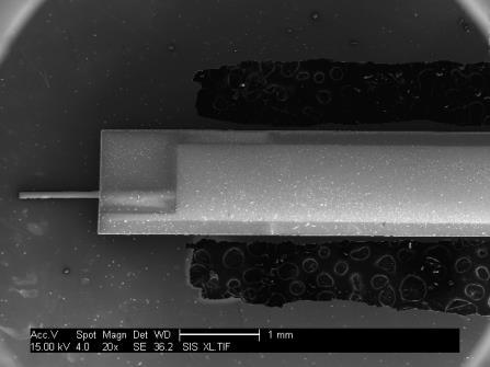
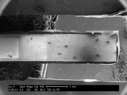
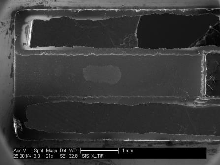
25 Piezoelectric energy harvesters PZT micro energy harvesting cantilever Thursday, 09 April
26 Performance Thursday, 09 April
27 Printed piezoelectrics & pyroelectrics Architecture Process Active material thickness (µm) Substrate thickness (µm) Dimensions L x W (mm) Power (µw) Power density (µw/cm 3 ) Operational frequency (Hz) Bimorph Screen 20 (x2) n/a 6.5 x g Bimorph Screen 55 none 18 x @0.5 g 227 Unimorph Screen 65 (x2) x Unimorph Screen ( ) x x Unimoph PSG/spin x 17 1 g 1 g 89 Unimorph Aerosol x g 1.5 g 112 Unimorph Tape cast x Pyroelectric Screen ~ 10-3 Thursday, 09 April
28 Printed piezoelectrics & pyroelectrics Architecture Process Active material thickness (µm) Substrate thickness (µm) Dimensions L x W (mm) Power (µw) Power density (µw/cm 3 ) Operational frequency (Hz) Bimorph Screen 20 (x2) n/a 6.5 x g Bimorph Screen 55 none 18 x @0.5 g 227 Unimorph Screen 65 (x2) x Unimorph Screen ( ) x x Unimoph PSG/spin x 17 1 g 1 g 89 Unimorph Aerosol x g 1.5 g 112 Unimorph Tape cast x Pyroelectric Screen ~ 10-3 Likely to be pw level Thursday, 09 April
29 Printed thermoelectrics Architecture Processing Active material thickness (µm) In-plane (n) (Bi,Sb) 2 Te) 3 (p) Bi 2 (Se,Te) 3 In-plane Elements Seebeck coef. (µv/k) ZT Power factor (α 2 σ) mw/m 2 K Screen Power density (µw/cm 3 ) (unimat) Bi 2 Te 3 (20 K ΔT) Dispenser RT Film only Screen (@RT) Bi 2 Te 3 Film only Ca 3 Co 4 O 9 Aerosol (@ C) Film only ZnSb Screen (@ K) Bi 0.85 Sb 0.15 /epoxy Screen 97 Ag-Ni Screen ~RT 30 Multilayer (n) LaSrTiO 3 (p) Ni-Mo In-plane (n) Bi 2 Te 3 (p) Sb 2 Te 3 Π Cu/Ni Multilayer (n) 100 (p) 25 Coevaporation Electroplate 50 (n) RT (p) RT - 8 (n) 248 (p) 188 (n) (p) (n) 300K (p) 300K (n) 300K (p) 300K (200 K ΔT) 450 (360 K ΔT) (0.12 K ΔT) - Thursday, 09 April
30 Summary Film based harvesters can be fabricated Thick films are reliant on consolidation of powders i.e. heat required Film forming techniques are continually improving Cheaper & quicker to fabricate than bulk systems Based on: Integrated Powder-based Thick Films for Thermoelectric, Pyroelectric and Piezoelectric Energy Harvesting Devices Robert A. Dorey IEEE Sensors Journal, vol 14, no 7, pp , 2014 Thursday, 09 April
31 Contact details Professor Robert Dorey Chair in Nanomaterials Department of Mechanical Engineering Sciences, Faculty of Engineering and Physical Sciences, University of Surrey Guildford Surrey UK GU2 7XH Ceramic Thick Films for MEMS and Microdevices ISBN: Thursday, 09 April
TFA Thin Film Analyzer
 TFA Thin Film Analyzer Thin Film Analyzer The LINSEIS Thin Film Analyzer is the perfect solution to characterize a broad range of thin film samples in a very comfortable and quick way. It is an easy to
The growth of patterned ceramic thin films from polymer precursor solutions Göbel, Ole
 University of Groningen The growth of patterned ceramic thin films from polymer precursor solutions Göbel, Ole IMPORTANT NOTE: You are advised to consult the publisher's version (publisher's PDF) if you
THIN FILM ANALYZER TFA
 T H E R M A L A N A L Y S I S THIN FILM ANALYZER TFA Since 1957 LINSEIS Corporation has been delivering outstanding service, know how and leading innovative products in the field of thermal analysis and
Ceramic and glass technology
 1 Row materials preperation Plastic Raw materials preperation Solid raw materials preperation Aging wet milling mastication Mixing seving Grain size reduction Milling Crushing Very fine milling Fine milling
Crack Prevention in NiCr-Alloys when Processed by AM (L-PB) William Jarosinski March 8, 2017
 William Jarosinski March 8, 2017") Crack Prevention in NiCr-Alloys when Processed by AM (L-PB) William Jarosinski March 8, 2017 Evolution into Metal Powders for AM Coating Service Since 1950s Metal Powders for AM A derivative of thermal
Crack Prevention in NiCr-Alloys when Processed by AM (L-PB) William Jarosinski March 8, 2017 Evolution into Metal Powders for AM Coating Service Since 1950s Metal Powders for AM A derivative of thermal
Surface Micromachining
 Surface Micromachining Outline Introduction Material often used in surface micromachining Material selection criteria in surface micromachining Case study: Fabrication of electrostatic motor Major issues
Low Cost PZT/Polymer Composites as a Sensor Material
 Low Cost PZT/Polymer Composites as a Sensor Material Umut GUNAYDIN, Celaletdin ERGUN Istanbul Technical University, Mechanical Engineering Department, Taksim Istanbul, TURKEY. Abstract This research aims
THE DEVELOPMENT OF THE MICRO-GENERATOR ON THE SUBSTRATE BASED THIN FILM
 Proceedings of MNHT2008 Micro/Nanoscale Heat Transfer International Conference January 6-9, 2008, Tainan, Taiwan MNHT2008-52198 THE DEVELOPMENT OF THE MICRO-GENERATOR ON THE SUBSTRATE BASED THIN FILM Jun-ichiro
Transducers and Arrays for Medical
 High Resolution Ultrasound Transducers and Arrays for Medical Imaging Applications Tim Button Applied Functional Materials Ltd Birmingham, UK T W Button, F Dauchy, L Garcia-Gancedo, Gancedo H Hughes, Y
Preprint - Mechatronics 2008, Le Grand-Bornand, France, May
 Potentialities of piezoresistive cantilever force sensors based on free standing thick films Hélène Debéda(*), Isabelle Dufour, Patrick Ginet, Claude Lucat University of Bordeaux 1, IMS Laboratory, 51
Photonic Drying Pulsed Light as a low Temperature Sintering Process
 Photonic Drying Pulsed Light as a low Temperature Sintering Process Lou Panico Xenon Corporation W E S T E R N M I C H I G A N U N I V E R S I T Y PRESENTATION OVERVIEW What is Printed Electronics Materials
Available online at ScienceDirect. Energy Procedia 55 (2014 )
") Available online at www.sciencedirect.com ScienceDirect Energy Procedia 55 (2014 ) 702 707 4th International Conference on Silicon Photovoltaics, SiliconPV 2014 Observation of the contact formation of
Available online at www.sciencedirect.com ScienceDirect Energy Procedia 55 (2014 ) 702 707 4th International Conference on Silicon Photovoltaics, SiliconPV 2014 Observation of the contact formation of
3D technologies for integration of MEMS
 3D technologies for integration of MEMS, Fraunhofer Institute for Electronic Nano Systems Folie 1 Outlook Introduction 3D Processes Process integration Characterization Sample Applications Conclusion Folie
Preparation and characterization of nanostructured thermoelectric materials
 QuickTime et un décompresseur TIFF (non compressé) sont requis pour visionner cette image. Preparation and characterization of nanostructured thermoelectric materials Laboratoire de Physique des Matériaux,
Producing Metal Parts
 Producing Metal Parts CNC vs. Additive Manufacturing www.3dhubs.com METAL KIT 2 Introduction This Kit discusses how to select the right manufacturing process for metal parts by comparing CNC and Additive
Project title: Materials and Devices for Piezoelectric Energy Harvesters
 Project title: Materials and Devices for Piezoelectric Energy Harvesters Team Members: Project Leader: Susan Trolier-McKinstry Graduate Students: Charles Yeager and Hong Goo Yeo Undergraduate Student:
Application of Coating Technology on the Zirconium-Based Alloy to Decrease High-Temperature Oxidation
 Application of Coating Technology on the Zirconium-Based Alloy to Decrease High-Temperature Oxidation Hyun-Gil Kim*, Il-Hyun Kim, Jeong-Yong Park, Yang-Hyun Koo, KAERI, 989-111 Daedeok-daero, Yuseong-gu,
Etching Mask Properties of Diamond-Like Carbon Films
 N. New Nawachi Diamond et al. and Frontier Carbon Technology 13 Vol. 15, No. 1 2005 MYU Tokyo NDFCT 470 Etching Mask Properties of Diamond-Like Carbon Films Norio Nawachi *, Akira Yamamoto, Takahiro Tsutsumoto
Piezoelectric Polycrystalline (PZT) Components and Wafers
 Components and Wafers") Piezoelectric Polycrystalline (PZT) Components and Wafers Industry Leading Piezoelectric Polycrystalline (PZT) Component Manufacturing and Engineering CTS offers high-performance piezoelectric materials
Piezoelectric Polycrystalline (PZT) Components and Wafers Industry Leading Piezoelectric Polycrystalline (PZT) Component Manufacturing and Engineering CTS offers high-performance piezoelectric materials
Surface micromachining and Process flow part 1
 Surface micromachining and Process flow part 1 Identify the basic steps of a generic surface micromachining process Identify the critical requirements needed to create a MEMS using surface micromachining
Lecture 5. SOI Micromachining. SOI MUMPs. SOI Micromachining. Silicon-on-Insulator Microstructures. Agenda:
 EEL6935 Advanced MEMS (Spring 2005) Instructor: Dr. Huikai Xie SOI Micromachining Agenda: SOI Micromachining SOI MUMPs Multi-level structures Lecture 5 Silicon-on-Insulator Microstructures Single-crystal
Thermoelectric Microcoolers for Thermal Management Applications
 Thermoelectric Microcoolers for Thermal Management Applications J.-P. Fleurial, A. Borshchevsky, M.A. Ryan, W. Phillips, E. Kolawa, T. Kacisch and R. Ewell Jet Propulsion Laboratory/California Institute
ADVANCED LTCC PROCESSES USING PRESSURE ASSISTED SINTERING
 ADVANCED LTCC PROCESSES USING PRESSURE ASSISTED SINTERING Heiko Thust Michael Hintz, Arne Albrecht Technical University of Ilmenau Ilmenau, Thuringia, Germany Heiko.thust@tu-ilmenau.de ABSTRACT Low Temperature
Lecture 6. Through-Wafer Interconnect. Agenda: Through-wafer Interconnect Polymer MEMS. Through-Wafer Interconnect -1. Through-Wafer Interconnect -2
 Agenda: EEL6935 Advanced MEMS (Spring 2005) Instructor: Dr. Huikai Xie Lecture 6 Through-wafer Interconnect EEL6935 Advanced MEMS 2005 H. Xie 1/21/2005 1 Motivations: Wafer-level packaging CMOS 3D Integration
SINTEF movemems. a standard process for piezoelectric microsystems prototyping
 SINTEF movemems a standard process for piezoelectric microsystems prototyping Frode Tyholdt Background Small and medium companies/ Universities have ideas for piezomems Difficult to make Need special tools
THE ASPECTS ABOUT RAPID PROTOTYPING SYSTEM
 THE ASPECTS ABOUT RAPID PROTOTYPING SYSTEM Adrian P. POP 1, Petru UNGUR 1, Gheorghe BEJINARU MIHOC 2 1 University of Oradea, e-mail: adippop@yahoo.com; petru_ungur@yahoo.com; 2 Transilvania University
Experimental O 3. Results and discussion
 Introduction Surface coatings to protect against oxidation extend the service temperature and the service life of basic metals. The commercially used coating systems can be divided into three main groups:
RAPID PATTERN BASED POWDER SINTERING TECHNIQUE AND RELATED SHRINKAGE CONTROL
 RAPID PATTERN BASED POWDER SINTERING TECHNIQUE AND RELATED SHRINKAGE CONTROL Jack G. Zhou and Zongyan He ABSTRACT Department of Mechanical Engineering and Mechanics Drexel University 3141 Chestnut Street
TIMAwave a novel test stand for thermal diffusivity measurement based on the Angstrom s method
 1 TIMAwave a novel test stand for thermal diffusivity measurement based on the Angstrom s method 12th European Advanced Technology Workshop on Micropackaging and Thermal management La Rochelle, France
Free standing Multilayer Thin Film of Cellulose Nanocrystals
 Free standing Multilayer Thin Film of Cellulose Nanocrystals Chaoyang Jiang Department of Chemistry The University of South Dakota Edmonton, June 25, 2009 Cellulose Nanocrystals Nanotechnology R&D Priority
 2007 PLACE Conference September 16-20 St Louis, MO Nano-Composite Polymer Optical Coatings Vampire Optical Coatings, Inc. Tom Faris vcoat@copper.net Introduction What is a nano-composite polymer coating?
Evaluation of an Environmentally Friendly Plasticizer For Polyvinyl Butyral For Use in Tape Casting
 Evaluation of an Environmentally Friendly Plasticizer For Polyvinyl Butyral For Use in Tape Casting Richard E. Mistler*, Ernest Bianchi**, Bruce Wade***, and Jeffrey Hurlbut*** Abstract: An environmentally
Arch. Metall. Mater. 62 (2017), 2B,
, 2B,") Arch. Metall. Mater. 62 (2017), 2B, 1225-1229 DOI: 10.1515/amm-2017-0182 S.S. KIM*, I. SON* #, K.T. KIM** EFFECT OF ELECTROLESS Ni P PLATING ON THE BONDING STRENGTH OF Bi Te-BASED THERMOELECTRIC MODULES
Arch. Metall. Mater. 62 (2017), 2B, 1225-1229 DOI: 10.1515/amm-2017-0182 S.S. KIM*, I. SON* #, K.T. KIM** EFFECT OF ELECTROLESS Ni P PLATING ON THE BONDING STRENGTH OF Bi Te-BASED THERMOELECTRIC MODULES
Development of Piezoelectric Nanocomposites for Energy Harvesting and Self-Sensing
 Development of Piezoelectric Nanocomposites for Energy Harvesting and Self- Kenneth J. Loh Assistant Professor Department of Civil & Environmental Engineering University of California, Davis The Applied
Vertically aligned Ni magnetic nanowires fabricated by diblock-copolymer-directed Al thin film anodization
 Vertically aligned Ni magnetic nanowires fabricated by diblock-copolymer-directed Al thin film anodization Researcher: Kunbae (Kevin) Noh, Graduate Student, MAE Dept. and CMRR Collaborators: Leon Chen,
PEC (Printed Electronic Circuit) process for LED interconnection
 process for LED interconnection") PEC (Printed Electronic Circuit) process for LED interconnection Higher wattage LED s/ power components or their placement in higher densities, requires a larger dissipation of heat in a more effective
PEC (Printed Electronic Circuit) process for LED interconnection Higher wattage LED s/ power components or their placement in higher densities, requires a larger dissipation of heat in a more effective
FGM Materials and Finding an Appropriate Model for the Thermal Conductivity
 Available online at www.sciencedirect.com Procedia Engineering 14 (2011) 3199 3204 The Twelfth East Asia-Pacific Conference on Structural Engineering and Construction FGM Materials and Finding an Appropriate
Piezoelectric Thick Film Technology Integrated Self-sustained Systems for Industrial
 InSensor Piezoelectric Thick Film Technology Integrated Self-sustained Systems for Industrial Applications Wanda W. Wolny, Rasmus Lou-Moeller, Erling Ringgaard, Konstantin Astafjev and Tomasz Zawada Meggitt
Fabrication of Magnesium Oxide Ceramics with Density Close to Theoretical Using Nanopowders
 Fabrication of Magnesium Oxide Ceramics with Density Close to Theoretical Using Nanopowders Jing Yang, Tzu-Chieh Lin, Bill Manett, Jeremy Young, Dan Rooney Eugene Medvedovski SCI Engineered Materials,
Annealing Behavior of Bi 2 Te 3 Thermoelectric Semiconductor Electrodeposited for Nanowire Applications
 Journal of the Korean Physical Society, Vol. 50, No. 3, March 2007, pp. 670 676 Annealing Behavior of Bi 2 Te 3 Thermoelectric Semiconductor Electrodeposited for Nanowire Applications Min-Young Kim and
Gaetano L Episcopo. Introduction to MEMS
 Gaetano L Episcopo Introduction to MEMS What are MEMS? Micro Electro Mechanichal Systems MEMS are integrated devices, or systems of devices, with microscopic parts, such as: Mechanical Parts Electrical
Supporting Information
 Supporting Information Fast-Response, Sensitivitive and Low-Powered Chemosensors by Fusing Nanostructured Porous Thin Film and IDEs-Microheater Chip Zhengfei Dai,, Lei Xu,#,, Guotao Duan *,, Tie Li *,,
37032 Tours Cedex 1, France e Cranfield University, Bedfordshire MK43 0AL, UK f University of Surrey, Surrey, GU2 7XH, UK
 Fabrication and characterization of annular-array, high-frequency, ultrasonic transducers based on PZT thick film D. Wang a, b, *, E. Filoux c, F. Levassort d, M. Lethiecq d, S.A. Rocks e and R.A. Dorey
Nano- And Micro-Filled Conducting Adhesives For Z-axis Interconnects
 Nano- And Micro-Filled Conducting Adhesives For Z-axis Interconnects We take a look at micro-filled epoxy-based conducting adhesives modified with nanoparticles for z- axis interconnections, especially
KGC SCIENTIFIC Making of a Chip
 KGC SCIENTIFIC www.kgcscientific.com Making of a Chip FROM THE SAND TO THE PACKAGE, A DIAGRAM TO UNDERSTAND HOW CPU IS MADE? Sand CPU CHAIN ANALYSIS OF SEMICONDUCTOR Material for manufacturing process
Viscosity, 25 C. Mn, g/mol. Wingtack
 Wingtack 10 A Unique Liquid Tackifying Resin Benefits Tackifying hydrocarbon resin Low-color liquid resin Broad compatibility Polymeric plasticization Enhanced flexibility Low-temperature tack and adhesion
Achieving premium product appeal. Metasheen Superior mirror and liquid metal effects
 Achieving premium product appeal Metasheen Superior mirror and liquid metal effects Agenda Metasheen at a glance Performance highlights Our global portfolio Guide formulations 2 Metasheen at a glance Metasheen
ZnO-based Transparent Conductive Oxide Thin Films
 IEEE EDS Mini-colloquium WIMNACT 32 ZnO-based Transparent Conductive Oxide Thin Films Weijie SONG Ningbo Institute of Material Technology and Engineering, Chinese Academy of Sciences, Ningbo, P. R. China
Contents. 1. Introduction to Materials Processing Starting Materials 21. Acknowledgements
 Preface Acknowledgements xiii xv 1. Introduction to Materials Processing 1 1.1 Materials Processing: Definition and Scope 1 1.2 Three Approaches to Materials Processing 4 1.3 Materials Processing Steps
Lecture 10: MultiUser MEMS Process (MUMPS)
") MEMS: Fabrication Lecture 10: MultiUser MEMS Process (MUMPS) Prasanna S. Gandhi Assistant Professor, Department of Mechanical Engineering, Indian Institute of Technology, Bombay, 1 Recap Various VLSI based
MEMS: Fabrication Lecture 10: MultiUser MEMS Process (MUMPS) Prasanna S. Gandhi Assistant Professor, Department of Mechanical Engineering, Indian Institute of Technology, Bombay, 1 Recap Various VLSI based
Microstructures using RF sputtered PSG film as a sacrificial layer in surface micromachining
 Sādhanā Vol. 34, Part 4, August 2009, pp. 557 562. Printed in India Microstructures using RF sputtered PSG film as a sacrificial layer in surface micromachining VIVEKANAND BHATT 1,, SUDHIR CHANDRA 1 and
Organic Solar Cells. Green River Project
 Organic Solar Cells Green River Project Silicon Cells Silicon semiconductors Advantages: Efficiencies Lifetimes Disadvantages: High manufacturing costs Inflexible http://en.wikipedia.org Organic semiconductors
ME 189 Microsystems Design and Manufacture. Chapter 9. Micromanufacturing
 ME 189 Microsystems Design and Manufacture Chapter 9 Micromanufacturing This chapter will offer an overview of the application of the various fabrication techniques described in Chapter 8 in the manufacturing
EXCIMER LASER ANNEALING FOR LOW- TEMPERATURE POLYSILICON THIN FILM TRANSISTOR FABRICATION ON PLASTIC SUBSTRATES
 EXCIMER LASER ANNEALING FOR LOW- TEMPERATURE POLYSILICON THIN FILM TRANSISTOR FABRICATION ON PLASTIC SUBSTRATES G. Fortunato, A. Pecora, L. Maiolo, M. Cuscunà, D. Simeone, A. Minotti, and L. Mariucci CNR-IMM,
Bronze Powder Research and Development for Cold Spray Repair
 Bronze Powder Research and Development for Cold Spray Repair Dan Kaplowitz, PhD Near Net Shape Processing Team US Army Research Laboratory Center for Cold Spray June 23, 2015 Cold Spray Action Team Meeting
Inkjet-Deposited Interconnections for Electronic Packaging
 Inkjet-Deposited Interconnections for Electronic Packaging Matti Mäntysalo and Pauliina Mansikkamäki, Tampere University of Technology, Korkeakoulunkatu 3, P.O.Box 692 FI-33101, Tampere, Finland, matti.mantysalo@tut.fi,
Specimen Preparation Technique for a Microstructure Analysis Using the Focused Ion Beam Process
 Specimen Preparation Technique for a Microstructure Analysis Using the Focused Ion Beam Process by Kozue Yabusaki * and Hirokazu Sasaki * In recent years the FIB technique has been widely used for specimen
Soft Lithography. Jin-Goo Park. Materials and Chemical Engineering Hanyang University, Ansan. Electronic Materials and Processing Lab.
 Hanyang University Soft Lithography Jin-Goo Park Materials and Chemical Engineering Hanyang University, Ansan Electronic Materials and Processing Lab. Introduction to Soft Lithography Research Micro- Electro-
Atomic Layer Deposition
 Atomic Layer Deposition Ville Malinen R&D Engineer Nanopinnoitteita koneenrakentajille 2010 1 Introduction 1) Overview of Beneq 2) Atomic Layer Deposition (ALD), to deposit thin films, which Are dense
MICROWAVE & RF MATERIALS GUIDE
 MICROWAVE & RF MATERIALS GUIDE RF & Microwave Materials Guide Arlon Microwave Materials specializes in products made from fluoropolymers (i.e. PTFE), ceramic-filled fluoropolymers, ceramic-filled hydrocarbon
Nanoparticles Improve Coating Performances
 Nanoparticles Improve Coating Performances presented by Dr. Thomas Sawitowski, Manager Nanotechnology The use of Nanoadditives in plastic and coating composites ICNT, San Francisco 2005 1 Out-line Definition
FUNDAMENTAL STUDY ON MICROSTRUCTURE OF CeO 2 -DOPED (Na 0.5 Bi 0.5 )TiO 3 CERAMICS
TiO 3 CERAMICS") FUNDAMENTAL STUDY ON MICROSTRUCTURE OF CeO 2 -DOPED (Na 0.5 Bi 0.5 )TiO 3 CERAMICS Rozidawati Awang 1,*, Nurain Ab. Halim 1, Zalita Zainuddin 1, Mohammad Hafizuddin Haji Jumali 1, Muhammad Yahaya 1 and
FUNDAMENTAL STUDY ON MICROSTRUCTURE OF CeO 2 -DOPED (Na 0.5 Bi 0.5 )TiO 3 CERAMICS Rozidawati Awang 1,*, Nurain Ab. Halim 1, Zalita Zainuddin 1, Mohammad Hafizuddin Haji Jumali 1, Muhammad Yahaya 1 and
3D inkjet printing of conductive structures using in-situ IR sintering
 3D inkjet printing of conductive structures using in-situ IR sintering E. Saleh*, J. Vaithilingam, C. Tuck, R. Wildman, I. Ashcroft, R. Hague, P. Dickens University of Nottingham, Additive Manufacturing
ENERGY CONVERSION USING NEW THERMOELECTRIC GENERATOR
 uthor manuscript, published in "N/P" Stresa, Italy, 6-8 pril 6 ENERGY CONVERSION USING NEW THERMOEECTRIC GENERTOR G. Savelli,, M. Plissonnier, J. Bablet, C. Salvi, J.M. Fournier, CE/ITEN/DTNM/CH, 7 rue
OPTIMISED CURING OF SILVER INK JET BASED PRINTED TRACES
 Nice, Côte d Azur, France, 27-29 September 2006 OPTIMISED CURING OF SILVER INK JET BASED PRINTED TRACES Z. Radivojevic 1, K. Andersson 1, K. Hashizume 2, M. Heino 1, M. Mantysalo 3, P. Mansikkamaki 3,
Tape Casting Formula Development. Polymer Innovations, Inc. Vista, CA USA Phone:
 Tape Casting Formula Development Polymer Innovations, Inc. Vista, CA 92081 USA www.polymerinnovations.com Phone: 760-598-0500 Formulation Steps Determine desired loading. Adjust formula for correct viscosity.
ITR Amorphous PLA for coating applications. TOYOBO CO.,LTD. Vylon Department Takashi Miyamoto
 ITR-2012 Amorphous PLA for coating applications TOYOBO CO.,LTD. Vylon Department Takashi Miyamoto CONTENTS 1. About TOYOBO 2. About VYLOECOL 1Key features 2Molecular design 3Grades and each specification
Industrial Coatings: HIGHLY DURABLE, SUPERHYDROPHOBIC AND OLEOPHOBIC. (White Paper) NeverWet LLC
 NeverWet LLC") Industrial Coatings: HIGHLY DURABLE, SUPERHYDROPHOBIC AND OLEOPHOBIC (White Paper) NeverWet LLC Background: Metal surfaces have high surface energy, are negatively charged, and hydrophilic as shown by
Industrial Coatings: HIGHLY DURABLE, SUPERHYDROPHOBIC AND OLEOPHOBIC (White Paper) NeverWet LLC Background: Metal surfaces have high surface energy, are negatively charged, and hydrophilic as shown by
Net-Shaping of Ceramic Components by Using Rapid Prototyping Technologies
 13 Net-Shaping of Ceramic Components by Using Rapid Prototyping Technologies Xiaoyong Tian 1, Dichen Li 1 and Jürgen G. Heinrich 2 1 Xi an Jiaotong University, Xi an, 2 Clausthal University of Technology,
80 Development of REBa2Cu3Ox Coated Conductor on Textured Metal Substrate
 ELECTRIC WIRE & CABLE, ENERGY Development of REBa2Cu3Ox Coated Conductor on Textured Metal Substrate Yuki SHINGAI*, Tatsuoki NAGAISHI, Masaya KONISHI, Hajime OTA, Takahiro TANEDA and Kazuya OHMATSU Sumitomo
MCC. PMGI Resists NANO PMGI RESISTS OFFER RANGE OF PRODUCTS
 MCC PMGI RESISTS OFFER Sub.25µm lift-off processing Film thicknesses from 5µm Choice of resin blends for optimal undercut control High thermal stability Superior adhesion to Si, NiFe, GaAs, InP
Production of PV cells
 Production of PV cells MWp 1400 1200 Average market growth 1981-2003: 32% 2004: 67% 1000 800 600 400 200 0 1991 1992 1993 1994 1995 1996 1997 1998 1999 2000 2001 2002 2003 2004 rest 1.0 1.0 1.0 2.0 4.0
Green piezoelectric for autonomous smart textile
 Journal of Physics: Conference Series PAPER OPEN ACCESS Green piezoelectric for autonomous smart textile To cite this article: E Lemaire et al 2015 J. Phys.: Conf. Ser. 660 012082 View the article online
Metal Matrix Composite (MMC)
") Matrix Metal Matrix Composite (MMC) The matrix is the monolithic material into which the reinforcement is embedded, and is completely continuous. This means thatt there is apath throughh the matrix ti
Matrix Metal Matrix Composite (MMC) The matrix is the monolithic material into which the reinforcement is embedded, and is completely continuous. This means thatt there is apath throughh the matrix ti
Thick films of YSZ electrolytes by dip-coating process
 Thick films of YSZ electrolytes by dip-coating process P. LENORMAND, D. CARAVACA, C. LABERTY-ROBERT, F. ANSART. Centre Inter-universitaire de Recherche et d Ingénierie sur les MATériaux, UMR 5085 Université
NanoSystemsEngineering: NanoNose Final Status, March 2011
 1 NanoSystemsEngineering: NanoNose Final Status, March 2011 The Nanonose project is based on four research projects (VCSELs, 3D nanolithography, coatings and system integration). Below, the major achievements
Room-Temperature Pressureless Bonding with Silver Nanowire. Paste: Towards Organic Electronic and Heat-Sensitive Functional
 Supplementary Materials Room-Temperature Pressureless Bonding with Silver Nanowire Paste: Towards Organic Electronic and Heat-Sensitive Functional Devices Packaging Peng Peng, a,b Anming Hu,* a Hong Huang,
HIGH TEMPERATURE CERAMIC & GRAPHITE ADHESIVES
 HIGH TEMPERATURE & GRAPHITE S Technical Bulletin A2 Ceramabond 835-M bonds halogen lamp. Ceramabond 503 coats heater used to 1700 ºC. Ceramabond 685-N bonds infrared heater. Graphi-Bond 551-RN bonds graphite
Powder Metallurgy. Science, Technology. and Materials. Anish Upadhyaya. G S Upadhyaya. Department of Materials Science and Engineering
 Powder Metallurgy Science, Technology and Materials Anish Upadhyaya Associate Professor Department of Materials Science and Engineering Indian Institute of Technology Kanpur, India G S Upadhyaya Former
Proceedings Post Fabrication Processing of Foundry MEMS Structures Exhibiting Large, Out-of-Plane Deflections
 Proceedings Post Fabrication Processing of Foundry MEMS Structures Exhibiting Large, Out-of-Plane Deflections LaVern Starman 1, *, John Walton 1, Harris Hall 1 and Robert Lake 2 1 Sensors Directorate,
BIOACTIVE SILICIUM-CONTAINING COATINGS ON TITANIUM SUBSTRATE
 Powder Metallurgy Progress, Vol.11 (2011), No 3-4 271 BIOACTIVE SILICIUM-CONTAINING COATINGS ON TITANIUM SUBSTRATE O. S. Antonova, V. V. Smirnov, S. M. Barinov, N. V. Bakunova, Ľ. Medvecký, J. Ďurišin
Metallization deposition and etching. Material mainly taken from Campbell, UCCS
 Metallization deposition and etching Material mainly taken from Campbell, UCCS Application Metallization is back-end processing Metals used are aluminum and copper Mainly involves deposition and etching,
Photolithography I ( Part 2 )
") 1 Photolithography I ( Part 2 ) Chapter 13 : Semiconductor Manufacturing Technology by M. Quirk & J. Serda Bjørn-Ove Fimland, Department of Electronics and Telecommunication, Norwegian University of Science
1 Photolithography I ( Part 2 ) Chapter 13 : Semiconductor Manufacturing Technology by M. Quirk & J. Serda Bjørn-Ove Fimland, Department of Electronics and Telecommunication, Norwegian University of Science
Laser assisted Cold Spray
 2009-02-16 Laser assisted Cold Spray Andrew Cockburn, Matthew Bray, Rocco Lupoi Bill O Neill Innovative Manufacturing Research Centre (IMRC) Institute for Manufacturing, Department of Engineering, University
SLID bonding for thermal interfaces. Thermal performance. Technology for a better society
 SLID bonding for thermal interfaces Thermal performance Outline Background and motivation The HTPEP project Solid-Liquid Inter-Diffusion (SLID) Au-Sn SLID Cu-Sn SLID Reliability and bond integrity Alternative
Nonplanar Metallization. Planar Metallization. Professor N Cheung, U.C. Berkeley
 Nonplanar Metallization Planar Metallization Passivation Metal 5 (copper) Metal 3 (copper) Interlevel dielectric (ILD) Via (tungsten) Metal 1 (copper) Tungsten Plug to Si Silicon Caps and Plugs oxide oxide
Barrier coating for food packaging
 CCMX, Neuchâtel, CSEM, March 26th, 2009 Barrier coating for food packaging Pierre Fayet Tetra Pak (Suisse) SA, Romont pierre.fayet@tetrapak.com Outlook: 1. Barrier coating technology 2. Mechanical characterization
In-situ atmosphere monitoring of the debinding of PM steel components with large amounts of organic additions
 In-situ atmosphere monitoring of the debinding of PM steel components with large amounts of organic additions October 12 th 216 Peter Quadbeck, Alexander Strauß, Bernd Kieback, Olaf Andersen Fraunhofer
Supplementary Figure S1 Crystal structure of the conducting filaments in sputtered SiO 2
 Supplementary Figure S1 Crystal structure of the conducting filaments in sputtered SiO 2 based devices. (a) TEM image of the conducting filament in a SiO 2 based memory device used for SAED analysis. (b)
Thermal Management Catalog
 Management Catalog P-THERM Interface Materials Polymer Science, Inc. offers a complete thermal management product line. Our P-THERM Interface Materials are designed to efficiently and effectively aid in
Atomic Layer Deposition(ALD)
") Atomic Layer Deposition(ALD) AlO x for diffusion barriers OLED displays http://en.wikipedia.org/wiki/atomic_layer_deposition#/media/file:ald_schematics.jpg Lam s market-leading ALTUS systems combine CVD
Atomic Layer Deposition(ALD) AlO x for diffusion barriers OLED displays http://en.wikipedia.org/wiki/atomic_layer_deposition#/media/file:ald_schematics.jpg Lam s market-leading ALTUS systems combine CVD
Thermal Management Catalog
 Management Catalog P-THERM Interface Materials Polymer Science, Inc. offers a complete thermal management product line. Our P-THERM Interface Materials are designed to efficiently and effectively aid in
Final Year Project Proposal 1
 Final Year Project Proposal 1 Mechanical testing for high temperature polymers Mr Eric Phua Jian Rong (JRPhua@ntu.edu.sg) In offshore subsea drilling, different types of microelectronics devices and sensors
Manufacturing of Metal Foam Supported SOFCs with Graded Ceramic Layer Structure and Thinfilm Electrolyte
 Manufacturing of Metal Foam Supported SOFCs with Graded Ceramic Layer Structure and Thinfilm Electrolyte Feng Han 1, Robert Semerad 2, and Rémi Costa 1 1 German Aerospace Center 2 Ceraco Ceramic Coating
Aluminum Nitride Thin Films for High Frequency Smart Ultrasonic Sensor Systems
 18th World Conference on Nondestructive Testing, 16-20 April 2012, Durban, South Africa Aluminum Nitride Thin Films for High Frequency Smart Ultrasonic Sensor Systems Thomas HERZOG, Susan WALTER, Susanne
High-Resolution, Electrohydrodynamic Inkjet Printing of Stretchable, Metal Oxide Semiconductor Transistors with High Performances
 Electronic Supplementary Material (ESI) for Nanoscale. This journal is The Royal Society of Chemistry 2016 ` Electronic Supplementary Information High-Resolution, Electrohydrodynamic Inkjet Printing of
Dicing Glass Optical Devices
 Glass Applications Dicing Glass Optical Devices -Blade Characteristics 2,, 4 4 Resin Type Q Diamond grit size: 15-45 mic. Thickness: 0.006-0.012 0.012 (0.15mm 0.3mm) Metal Sintered E08 & New matrices 8-258
FABRICATION PROCESSES FOR MAGNETIC MICROACTUATORS WITH POLYSILICON FLEXURES. Jack W. Judy and Richard S. Muller
 FABRICATION PROCESSES FOR MAGNETIC MICROACTUATORS WITH POLYSILICON FLEXURES Jack W. Judy and Richard S. Muller Berkeley Sensor & Actuator Center (BSAC) Department of EECS, University of California, Berkeley,
THERMAL CONDUCTION OF NANO-DIAMOND DISPERSED POLYURETHANE NANO-COMPOSITES
 THERMAL CONDUCTION OF NANO-DIAMOND DISPERSED POLYURETHANE NANO-COMPOSITES Andrew P Limmack and Dr H-X Peng ACCIS, University of Bristol Department of Aerospace Engineering Queens Building, University Walk,