Semiconductor devices for display and memory application
|
|
|
- Duane Walters
- 5 years ago
- Views:
Transcription
1 Semiconductor devices for display and memory application Chungnam National University April 18, 2014 Gawon Lee 1
2 Contents 1. Semiconductor Engineering Lab. 2. Oxide Thin Film Transistors 2.1 Introduction 2.2 Thin Film Transistor (TFT) 2.3 Oxide TFT for Display application 3. NVM: SONOS Flash Memory 3.1 Introduction 3.2 Silicon-Oxide-Nitride-Oxide-Silicon (SONOS) Flash Memory 3.3 SONOS Technology 2
 홈페이지 : http://www.")

3 Semiconductor Engineering Laboratory 학생현황 : 석사 5 명 / 박사 4 명 (2014 년 4 월 ) 홈페이지 : cnu.ac.kr/~semieng, gawon@cnu.ac.kr 주요연구분야차세대디스플레이셀구동용박막트랜지스터연구차세대고성능플래쉬메모리연구이종접합태양전지 3
 S/D Contact Homogeneous contact using AZO TCO Interface control Passivation High-k dielectric New Merged Device Using nano-particle Characterization Tool Development 1/f Noise Analysis 도입")
4 Oxide TFT Research Field Fabrication Analysis Stability TFT Structure Schottky contact adoption to suppress back channel Channel Engineering New cation adoption (Ti) Gate Insulator High-k dielectric (Al2O3) S/D Contact Homogeneous contact using AZO TCO Interface control Passivation High-k dielectric New Merged Device Using nano-particle Characterization Tool Development 1/f Noise Analysis 도입 Pulsed IV method Simulation Feedback to mechanism model Potential distribution Dominant current path Bias Stability Hump Analysis focusing on ion movement Illumination Stability V Th focusing on oxygen vacancy (V O ) model 4

5 Flash Memory Research Field Fabrication Analysis Stability SONOS Structure 2D structure 3D structure Retention/Reliability Degradation Mech. Tunneling Ox. Engineering N2 implant adoption Trapping layer High-k dielectric New NVM Device Using nano-particle Transparent flexible NVM Characterization Tool Development Charge pumping method 1/f Noise Analysis Simulation Interface trap effect Structure effect (Rounding effect in 3D) 5
6 Flexible transparent Display/Device Application: Oxide Thin Film Transistors 6

7 Introduction: Flexible Transparent Display 7


8 Introduction: Flexible Transparent Display Flexible display : cell phone, PDA, laptop, e-book,wearable lightweight, low power consumption, bendable 8

9 Introduction: Flexible Transparent Display 얇고가볍고전력소비효율이높고깨지지않는투명하고유연한특성이중요해짐. Notebook, monitor, digital TV market, E-book application 현재 display 소자에사용되고있는 a-si, poly-si 의단점을극복할수있는 (High Temp. Process, Low Performance, 낮은광투과도등 ) 새로운전자소자개발필요성극대화 9
10 Introduction: Short History of Thin Film Transistors Julius Edgar Lilienfeld US "Method and apparatus for controlling electric current" first filed in Canada on (1930), describing a device similar to a MESFET US "Device for controlling electric current" filed on , a thin film MOSFET US "Amplifier for electric currents" filed on , solid state device where the current flow is controlled by a porous metal layer, a solid state version of the vacuum tube US "Electrolytic condenser" filed on , Electrolytic capacitor From Thin Film Transistor Technology Past, Present, and Future, The Electrochemical Society Interface (Spring 2013) 10

11 Introduction: Short History of Thin Film Transistors From Transparent Electronics: From Synthesis to Applications, Wiley 11


12 Introduction: Short History of Thin Film Transistors From Transparent Electronics: From Synthesis to Applications, Wiley 12

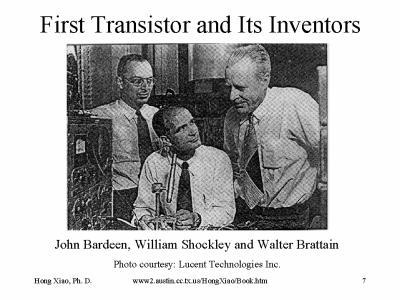
13 Introduction: Short History of Thin Film Transistors 트랜지스터발명가,Bardeen,Schockley,Brattain 게르마늄단결정으로만든최초의 BJT 13

14 Thin Film Transistor : Definition TFT: 절연성기판위에형성된 Field Effect Transistor A voltage applied at the gate controls the flow of electrons (resistance) from the source to the drain; a positive gate voltage attracts electrons to the bottom surface of the semiconductor layer and creates a conduction channel. When a voltage difference is applied between the two connector wires, electrons enter at one end (the source) and exit at the other (the drain), resulting in a current along the channel. Figure from 14
, which causes flexible electronics but limits the process temperature and deposition method.")
15 Thin Introduction Film Transistor: Structure - A common substrate is glass, since the primary application of TFTs is in liquid crystal displays while the conventional substrate of transistor is silicon wafer. But any substrate can be used (glass, polymer sheets, steel foils..), which causes flexible electronics but limits the process temperature and deposition method. - By using transparent semiconductors and transparent electrodes, such as indium tin oxide (ITO), some TFT devices can be made completely transparent 15

16 Thin Introduction Film Transistor: Structure A thin-film transistor (TFT) - Special kind of field-effect transistor made by depositing thin films of a semiconductor active layer as well as the dielectric layer and metallic contacts over a supporting substrate. 16

17 Introduction Thin Film Transistor: Manufacture Topside resist backside exposure Cr-gate has been patterned on the glass substrate PECVD gate oxide a-si:h channel and nitride stopper layers have been deposited. Nitride etching and resist stripping Chrominu sputtering CrSi2 formation. 17
18 Introduction Thin Film Transistor: Manufacture - Material Silicon : amorphous silicon, microcrystalline silicon, poly-silicon. Compound semiconductors: cadmium selenide, metal oxides such as zinc oxide Organic materials - Process Temperature Substrates cannot withstand high annealing temperatures, the deposition process has to be completed under relatively low temperatures. - Thin Film Deposition/Formation Process Chemical vapor deposition (CVD, ALD) Physical vapor deposition (Sputtering, Evaporation, MBE) Solution-coating process (Printing) 18
 - Switching transistor/diode -")
19 Thin Film Transistor for Display Application Active Matrix Liquid Crystal Display (AMLCD) - Switching transistor/diode - 19

20 Thin Film Transistor for Display Application Structure of TFT-AMLCD : Color TFT Panel 20

21 Thin Film Transistor for Display Application Appendix) TFT-LCD 제작용유리기판사이즈 Need for Uniformity and Low Temperature Process 21

22 Thin Film Transistor for Display Application OLED Structure Need for High mobility and Uniformity 22

23 Thin Film Transistor for Display Application AM OLED Structure 23

24 Oxide TFT for Display Application A-Si TFT LTPS TFT Oxide TFT Semiconductor Amorphous Si Poly Si Oxide Process (TFT) 4~5 mask 5~9 mask 4~5 mask Mobility <1cm 2 /V-s 50~150cm 2 /V-s 1~80 cm 2 /V-s TFT uniformity Good Poor Good Cost Cost/Yield Low/High High/Low Low/High Process Temp. ~250 o C >250 o C RT~300 o C Display Mode LCD, OLED LCD, OLED (Small size) LCD, OLED Substrate Glass Glass Glass, Plastic 경제성, 성능그리고신뢰성이모두확보되는기술이필수적 Si 을근간으로하는 TFT 의경우낮은이동도가문제 ( 대형 TFT 의성능을만족시킬만큼높지않다 ) Si 자체가가시광 [ 가시광선의에너지 (~3.1eV)] 영역을흡수 ( 차단 ) 하기때문에화면의휘도가낮아짐 유기물사용의경우아직도재료및공정등이초기기술상태이며향후에도신뢰성확보가쉽지않을것으로예상 Oxide TFT 는현재의 AMLCD 및 AMOLED 에서사용되고있는 Si-based TFT 를대체하여고성능소자제작가능 24
25 Oxide TFT for Display Application Source: IDTechEx 25

26 Oxide TFT for Display Application LTPS and Oxide TFT Backplane Manufacturing Capacity Source: 2013 NPD DisplaySearch TFT LCD Process Roadmap Report 26
 - SGZO(SnO 2 -Ga 2 O 3 -ZnO) IGZO")
27 Oxide TFT for Display Application Material Binary compound - ZnO - SnO 2 - In 2 O 3 Ternary compound - IZO, ZTO, IGO - AZO, GZO (TCO) ZnO가가장안정적인특성. In2O3가 bixbyite 구조로 octahedral site를공유함으로인해 high-mobility의특성을보임 3족원소인 Ga, Al을첨가하여 carrier concentration control Quaternary compound - IGZO(In 2 O 3 -Ga 2 O 3 -ZnO) - SGZO(SnO 2 -Ga 2 O 3 -ZnO) IGZO 는상온에서 Amorphous 구조이나, High-mobility 특성을나타냄. - bixbyite 구조 : 산소일부가부족한구조, Oxygen vacancy 의농도가높기때문에 ionic conductivity 가높다 27
28 Oxide TFT for Display Application Material: ZnO The ZnO channel TFTs exhibit better performance (higher field-effect mobility) than organic and a-si:h TFTs Resource availability (Low cost material) Non-toxicity Direct, Wide bandgap energy (3.4eV) -> High transmittance High exciton binding energy(60 mev) Low temp./inexpensive growth Easily etched (acids and alkalis) Thermal, chemical, Radiation stability Current Problems N-type only because of Oxygen vacancy and Zinc interstitial High performance TFTs with stability and uniformity 29

29 Oxide TFT for Display Application Appendix) Zinc interstitial in ZnO Zn Zn - Zn - Ec Zn 2n Zn + +e - Zn + Zn ++ +e - Zn 2n Zni ++ +2e - n-type Ev Eg=3.36eV Zni=2.9eV 30
 Oxygen vacancy in ZnO Vo")
 Vo 2 e Zn")

30 Oxide TFT for Display Application Appendix) Oxygen vacancy in ZnO Vo O 2 는높은휘발성에의해 Vacancy 생성 Zn O O O 2-2 ( ZnO 2 gas) Vo 2 e Zn dangling bonds each contributing 1/2 electron to a neutral vacancy 31
31 Oxide TFT for Display Application Material: a-igzo + Gallium Covalent bond length Ga-O = 1.92 Å Zn-O = 1.97 Å No deformation of the ZnO lattice High concentration of Ga + Indium Indium-gallium-zinc oxide Indium-zinc oxide Heavy metal cations Lower processing temperature, Good uniformity / reproducibility High mobility 32

32 Oxide TFT for Display Application Material: a-igzo 33
33 Oxide TFT for Display Application Material: a-igzo Improvement of optical characteristic and resistivity Low temperature deposition and good film smoothness, uniformity (amorphous oxides have more uniform structures and smoother surfaces) High performance (In spite of the amorphous structure, these oxides have relatively high electron mobility because Gallium Indium) 34
34 Nonvolatile Memory: Silicon-Oxide-Nitride-Oxide-Silicon Flash Memory 35

35 Introduction: Standard semiconductor memories Referred From Doo Seok Jeong, et. al., Emerging memories: resistive switching mechanisms and current status, Rep. Prog. Phys. 75 (2012) 36

36 Introduction: Storage capacitor of NVM s Image from 37

37 Introduction: NAND Flash Roadmap Image from 38


38 SONOS Flash Memory : Structure 39
")
39 SONOS Flash Memory : Basic Mechanism NOR vs. NAND type Flash Memory Similar Structure with DRAM Structure (Higher Density) Picture from Samsung Flash Seminar 40
40 SONOS Flash Memory : Basic Mechanism NAND Type: Program Method Picture from Samsung Flash Seminar 41
41 SONOS Flash Memory : Basic Mechanism NAND Type: Read Method Picture from Samsung Flash Seminar 42
42 SONOS Flash Memory : Basic Mechanism NAND Type: Program/Erase Method Picture from Samsung Flash Seminar 43


43 SONOS Flash Memory : Structure 44
 - High Erase speed (easy tunneling through thin bottom oxide) Referred from")
 Flash Memory and Study of the Gate-Stack Scaling")
44 SONOS Tech: Bandgap-Engineered (BE) SONOS - Tunnel oxide is replaced by triple layers of ultrathin ONO - Good data retention (charges are blocked by the total ONO barrier) - High Erase speed (easy tunneling through thin bottom oxide) Referred from Szu-Yu Wang et al., Reliability and Processing Effects of Bandgap-Engineered SONOS (BE-SONOS) Flash Memory and Study of the Gate-Stack Scaling Capability, IEEE Transactions on Device and Materials Reliability, Volume 8, Issue 2, June 2008 Page(s):
45 SONOS Tech: BE-SONOS : Gradual Variation of relative S/N ration (Tapered Bandgap Nitride Layer) Key Idea : The small barrier heights between nitride and the surrounding oxides have rendered the charges that enter nitride slip away easily and result in a poor charge-trapping efficiency. In addition, the deep trapping levels of standard nitride also make it difficult to catch carriers. 46

46 SONOS Tech: TANOS (SANOS) Band Diagram of SONOS and SANOS TaN Gate AL2O3 SiN Tunnel Oxide N + N + High-K dielectric for blocking oxide Low-voltage operation Possible to use thicker tunnel oxide High work function of TaN decrease of electron injection from gate during FN erase operation 47

47 SONOS Tech: 3D SONOS Technology 3D Structure: Technology Direction of NAND flash 48

 P-BiCS Structure (2009,")
48 SONOS Tech: 3D SONOS Technology BiCS Structure (2007, VLSI Symp.) P-BiCS Structure (2009, VLSI Symp.) 49


49 SONOS Tech: 3D SONOS Technology TCAT Structure (2009, VLSI Symp.) 50
50 Summary 1. Oxide Thin Film Transistor (Most promising candidate for next-generation display) Low Temperature Process/High Performance/Transparent/Low cost Material: IGZO and ZnO Issue: Bias/Optical Stability is required to be improved 2. SONOS (Promising candidate for NVM device) Scaling Limits of FG Flash Memory Tunneling Oxide Thickness/GCR/Floating Gate Interference (Crosstalk) SONOS Technology Trade-off between P/E speed and Data retention Gate Stack Optimization (TANOS, BE-SONOS, etc.) New Structure (3D structure) 51
Amorphous Oxide Transistor Electrokinetic Reflective Display on Flexible Glass
 Amorphous Oxide Transistor Electrokinetic Reflective Display on Flexible Glass Devin A. Mourey, Randy L. Hoffman, Sean M. Garner *, Arliena Holm, Brad Benson, Gregg Combs, James E. Abbott, Xinghua Li*,
Lecture 7 Metal Oxide Semiconductors
 Lecture 7 Metal Oxide Semiconductors 1/73 Announcements Homework 1/4: I will return it next Tuesday (October 16 th ). Homework 2/4: Will be online on later today. Due Thursday October 18 th at the start
Yung-Hui Yeh, and Bo-Cheng Kung Display Technology Center (DTC), Industrial Technology Research Institute, Hsinchu 310, Taiwan
, Industrial Technology Research Institute, Hsinchu 310, Taiwan") Amorphous In 2 O 3 -Ga 2 O 3 -ZnO Thin Film Transistors and Integrated Circuits on Flexible and Colorless Polyimide Substrates Hsing-Hung Hsieh, and Chung-Chih Wu* Graduate Institute of Electronics Engineering,
Amorphous In 2 O 3 -Ga 2 O 3 -ZnO Thin Film Transistors and Integrated Circuits on Flexible and Colorless Polyimide Substrates Hsing-Hung Hsieh, and Chung-Chih Wu* Graduate Institute of Electronics Engineering,
Study on the hydrogenated ZnO-based thin film transistors
 Final Report Study on the hydrogenated ZnO-based thin film transistors To Dr. Gregg Jessen Asian Office of Aerospace Research & Development April 30th, 2011 Jae-Hyung Jang School of Information and Communications
A Novel Low Temperature Self-Aligned Field Induced Drain Polycrystalline Silicon Thin Film Transistor by Using Selective Side-Etching Process
 Chapter 3 A Novel Low Temperature Self-Aligned Field Induced Drain Polycrystalline Silicon Thin Film Transistor by Using Selective Side-Etching Process 3.1 Introduction Low-temperature poly-si (LTPS) TFTs
2-1 Introduction The demand for high-density, low-cost, low-power consumption,
 Chapter 2 Hafnium Silicate (HfSi x O y ) Nanocrystal SONOS-Type Flash Memory Fabricated by Sol-Gel Spin Coating Method Using HfCl 4 and SiCl 4 as Precursors 2-1 Introduction The demand for high-density,
Lecture Day 2 Deposition
 Deposition Lecture Day 2 Deposition PVD - Physical Vapor Deposition E-beam Evaporation Thermal Evaporation (wire feed vs boat) Sputtering CVD - Chemical Vapor Deposition PECVD LPCVD MVD ALD MBE Plating
Summary and Scope for further study
 Chapter 6 Summary and Scope for further study 6.1 Summary of the present study Transparent electronics is an emerging science and technology field concentrated on fabricating invisible electronic circuits
Influence of Plasma Treatment to the Performance of Amorphous IGZO based Flexible Thin Film Transistors
 Article Influence of Plasma Treatment to the Performance of Amorphous IGZO based Flexible Thin Film Transistors Long-long Chen, Xiang Sun, Ji-feng Shi, Xi-feng Li *, Xing-wei Ding and Jian-hua Zhang *
行政院國家科學委員會補助專題研究計畫成果報告
 NSC89-2215-E-009-104 89 08 01 90 07 31 Fabrication and Characterization of Low-Temperature Polysilicon Thin Film Transistors with Novel Self-Aligned Sub-Gate Structures NSC89-2215-E009-104 (FID) self-aligned
1. Aluminum alloys for direct contacts. 1.1 Advantages of aluminum alloys for direct contacts
 Direct contacts between aluminum alloys and thin film transistors (TFTs) contact layers were studied. An Al-Ni alloy was found to be contacted directly with an indium tin oxide (ITO) layer successfully
Chapter 3 Silicon Device Fabrication Technology
 Chapter 3 Silicon Device Fabrication Technology Over 10 15 transistors (or 100,000 for every person in the world) are manufactured every year. VLSI (Very Large Scale Integration) ULSI (Ultra Large Scale
Doping and Oxidation
 Technische Universität Graz Institute of Solid State Physics Doping and Oxidation Franssila: Chapters 13,14, 15 Peter Hadley Technische Universität Graz Institute of Solid State Physics Doping Add donors
TANOS Charge-Trapping Flash Memory Structures
 TANOS Charge-Trapping Flash Memory Structures A Senior Design by Spencer Pringle 5/8/15 Table of Contents Motivation Why Charge-Trapping Flash (CTF)? Charge-Trapping vs. Floating Gate Electronically-Erasable
Amorphous and Polycrystalline Thin-Film Transistors
 Part I Amorphous and Polycrystalline Thin-Film Transistors HYBRID AMORPHOUS AND POLYCRYSTALLINE SILICON DEVICES FOR LARGE-AREA ELECTRONICS P. Mei, J. B. Boyce, D. K. Fork, G. Anderson, J. Ho, J. Lu, Xerox
Semiconductor Device Fabrication
 5 May 2003 Review Homework 6 Semiconductor Device Fabrication William Shockley, 1945 The network before the internet Bell Labs established a group to develop a semiconductor replacement for the vacuum
Microelectronics Devices
 Microelectronics Devices Yao-Joe Yang 1 Outline Basic semiconductor physics Semiconductor devices Resistors Capacitors P-N diodes BJT/MOSFET 2 Type of Solid Materials Solid materials may be classified
Simulation study on the active layer thickness and the interface of a-igzo-tft with double active layers
 Front. Optoelectron. 2015, 8(4): 445 450 DOI 10.1007/s12200-014-0451-1 RESEARCH ARTICLE Simulation study on the active layer thickness and the interface of a-igzo-tft with double active layers Xiaoyue
Encapsulation of Indium-Gallium-Zinc Oxide Thin Film Transistors
 Encapsulation of Indium-Gallium-Zinc Oxide Thin Film Transistors Encapsulation Layer Al gate Source IGZO Gate Drain Si JULIA OKVATH HIRSCHMAN RESEARCH GROUP @ RIT MAY 9, 2017 Outline Brief Introduction
The Mobility Enhancement of Indium Gallium Zinc Oxide Transistors via Low-temperature Crystallization using a Tantalum Catalytic Layer
 www.nature.com/scientificreports Received: 27 February 2017 Accepted: 24 August 2017 Published: xx xx xxxx OPEN The Mobility Enhancement of Indium Gallium Zinc Oxide Transistors via Low-temperature Crystallization
Chapter 4. UEEP2613 Microelectronic Fabrication. Oxidation
 Chapter 4 UEEP2613 Microelectronic Fabrication Oxidation Prepared by Dr. Lim Soo King 24 Jun 2012 Chapter 4...113 Oxidation...113 4.0 Introduction... 113 4.1 Chemistry of Silicon Dioxide Formation... 115
Charge-trap memories with high-k control dielectrics
 Charge-trap memories with high-k control dielectrics Gabriel Molas CEA-LETI MINATEC Advanced Memory Technology gabriel.molas@cea.fr G. Molas Workshop on Innovative Memory Technologies June 24 th 2009 1
Sputtering Target of Oxide Semiconductor with High Electron Mobility and High Stability for Flat Panel Displays
 ELECTRONICS Sputtering Target of Oxide Semiconductor with High Electron Mobility and High Stability for Flat Panel Displays Miki MIYANAGA*, Kenichi WATATANI, and Hideaki AWATA ----------------------------------------------------------------------------------------------------------------------------------------------------------------------------------------------------------------------------------------------------------
Silicon germanium photo-blocking layers for a-igzo based industrial display
 www.nature.com/scientificreports Received: 8 June 2018 Accepted: 23 October 2018 Published: xx xx xxxx OPEN Silicon germanium photo-blocking layers for a-igzo based industrial display Su Hyoung Kang 1,
Lecture 22: Integrated circuit fabrication
 Lecture 22: Integrated circuit fabrication Contents 1 Introduction 1 2 Layering 4 3 Patterning 7 4 Doping 8 4.1 Thermal diffusion......................... 10 4.2 Ion implantation.........................
The next thin-film PV technology we will discuss today is based on CIGS.
 ET3034TUx - 5.3 - CIGS PV Technology The next thin-film PV technology we will discuss today is based on CIGS. CIGS stands for copper indium gallium selenide sulfide. The typical CIGS alloys are heterogeneous
Organic Light-Emitting Diodes. By: Sanjay Tiwari
 Organic Light-Emitting Diodes By: Sanjay Tiwari Inorganic Vs. Organic Material Properties Limitations At Early Stage Organic materials have often proved to be unstable. Making reliable electrical contacts
OXIDE SEMICONDUCTOR thin-film transistors (TFTs)
") JOURNAL OF DISPLAY TECHNOLOGY, VOL. 8, NO. 1, JANUARY 2012 35 Effect of Self-Assembled Monolayer (SAM) on the Oxide Semiconductor Thin Film Transistor Seung-Hwan Cho, Yong-Uk Lee, Jeong-Soo Lee, Kang-Moon
JOURNAL OF DISPLAY TECHNOLOGY, VOL. 8, NO. 1, JANUARY 2012 35 Effect of Self-Assembled Monolayer (SAM) on the Oxide Semiconductor Thin Film Transistor Seung-Hwan Cho, Yong-Uk Lee, Jeong-Soo Lee, Kang-Moon
ZnO-based Transparent Conductive Oxide Thin Films
 IEEE EDS Mini-colloquium WIMNACT 32 ZnO-based Transparent Conductive Oxide Thin Films Weijie SONG Ningbo Institute of Material Technology and Engineering, Chinese Academy of Sciences, Ningbo, P. R. China
RECONFIGURABLE NEUROMORPHIC SYNAPSE INTERCONNECTS WITH TFT
 RECONFIGURABLE NEUROMORPHIC SYNAPSE INTERCONNECTS WITH TFT JAN GENOE PUBLIC Every neuron in a human brain is connected via its synapses to 10-15.000 other neurons. Those connections can be over time reconfigured
Effect of Ti/Cu Source/Drain on an Amorphous IGZO TFT Employing SiNx Passivation for Low Data-Line Resistance
 Effect of Ti/Cu Source/Drain on an Amorphous IGZO TFT Employing SiNx Passivation for Low Data-Line Resistance Young Wook Lee, Sun-Jae Kim, Soo-Yeon Lee, Woo-Geun Lee, Kap-Soo Yoon, Jae-Woo Park, Jang-Yeon
The Potential of Photovoltaics
 The Potential of Photovoltaics AIMCAL 2008 2008 Fall Conference Vacuum Web Coating Brent P. Nelson October 22, 2008 NREL is a national laboratory of the U.S. Department of Energy Office of Energy Efficiency
Effect of Post-Deposition Treatment on Characteristics of P-channel SnO
 Effect of Post-Deposition Treatment on Characteristics of P-channel SnO Thin-Film Transistors 1 Byeong-Jun Song, 2 Ho-Nyeon Lee 1, First Author Department of Electric & Robotics Engineering, Soonchunhyang
VLSI. Lecture 1. Jaeyong Chung System-on-Chips (SoC) Laboratory Incheon National University. Based on slides of David Money Harris
 Laboratory Incheon National University. Based on slides of David Money Harris") VLSI Lecture 1 Jaeyong Chung System-on-Chips (SoC) Laboratory Incheon National University Based on slides of David Money Harris Goals of This Course Learn the principles of VLSI design Learn to design
VLSI Lecture 1 Jaeyong Chung System-on-Chips (SoC) Laboratory Incheon National University Based on slides of David Money Harris Goals of This Course Learn the principles of VLSI design Learn to design
Lecture 0: Introduction
 Lecture 0: Introduction Introduction Integrated circuits: many transistors on one chip. Very Large Scale Integration (VLSI): bucketloads! Complementary Metal Oxide Semiconductor Fast, cheap, low power
Silicon Epitaxial CVD Want to create very sharp PN boundary grow one type layer on other in single crystal form High dopant layers on low dopant
 Silicon Epitaxial CVD Want to create very sharp PN boundary grow one type layer on other in single crystal form High dopant layers on low dopant substrate Creates latch up protection for CMOS Buried Epi
CMOS Processing Technology
 CHAPTER 2 CMOS Processing Technology Outline 2 1. CMOS Technologies 2. Layout Design Rules 3. CMOS Process Enhancements 4. Technology-related CAD Issues 5. Manufacturing Issues CMOS Technologies 3 n-well
CMOS Processing Technology
 CHAPTER 2 CMOS Processing Technology Outline 2 1. CMOS Technologies 2. Layout Design Rules 3. CMOS Process Enhancements 4. Technology-related CAD Issues 5. Manufacturing Issues CMOS Technologies 3 n-well
Silicon Epitaxial CVD Want to create very sharp PN boundary grow one type layer on other in single crystal form High dopant layers on low dopant
 Silicon Epitaxial CVD Want to create very sharp PN boundary grow one type layer on other in single crystal form High dopant layers on low dopant substrate Creates latch up protection for CMOS Buried Epi
EE 330 Lecture 8. IC Fabrication Technology Part II. - Oxidation - Epitaxy - Polysilicon - Interconnects
 EE 330 Lecture 8 IC Fabrication Technology Part II - Oxidation - Epitaxy - Polysilicon - Interconnects Review from Last Time MOS Transistor Bulk Source Gate Drain p-channel MOSFET Lightly-doped n-type
Activities in Plasma Process Technology at SENTECH Instruments GmbH, Berlin. Dr. Frank Schmidt
 Activities in Plasma Process Technology at SENTECH Instruments GmbH, Berlin Dr. Frank Schmidt The Company Company Private company, founded 1990 80 employees ISO 9001 Location Science & Technology Park,
ABSTRACT. LUO, HAOJUN. Amorphous Indium Gallium Zinc Oxide Based Thin Film Transistors and Circuits. (Under the direction of Dr. John Muth.
 ABSTRACT LUO, HAOJUN. Amorphous Indium Gallium Zinc Oxide Based Thin Film Transistors and Circuits. (Under the direction of Dr. John Muth.) The goal of this dissertation is to develop high performance
Chapter 3. In this chapter, we use sol-gel method to combine three high-k precursors, i.e. HfCl 4, ZrCl 4 and SiCl 4 together to form hafnium silicate
 Chapter 3 Sol-Gel-Derived Zirconium Silicate (ZrSi x O y ) and Hafnium Silicate (HfSi x O y ) Co-existed Nanocrystal SONOS Memory 3-1 Introduction In the previous chapter, we fabricate the sol-gel-derived
VLSI Systems and Computer Architecture Lab
 ΚΥΚΛΩΜΑΤΑ VLSI Πανεπιστήμιο Ιωαννίνων CMOS Technology Τμήμα Μηχανικών Η/Υ και Πληροφορικής 1 From the book: An Introduction ti to VLSI Process By: W. Maly ΚΥΚΛΩΜΑΤΑ VLSI Διάρθρωση 1. N well CMOS 2. Active
Atomic Layer Deposition (ALD)
") Atomic Layer Deposition (ALD) ALD provides Uniform, controlled, conformal deposition of oxide, nitride, and metal thin films on a nanometer scale. ALD is a self limiting thin film deposition technique
Atomic Layer Deposition (ALD) ALD provides Uniform, controlled, conformal deposition of oxide, nitride, and metal thin films on a nanometer scale. ALD is a self limiting thin film deposition technique
AN ABSTRACT OF THE DISSERTATION OF. Electrical and Computer Engineering presented on November 5, John F. Wager
 AN ABSTRACT OF THE DISSERTATION OF David Hong for the degree of Doctor of Philosophy in Electrical and Computer Engineering presented on November 5, 2008. Title: Fabrication and Characterization of Thin-film
Photovoltaics & Solar Thermals. Thin-film equipment. Customized. FHR Anlagenbau GmbH I
 Photovoltaics & Solar Thermals Thin-film equipment. Customized. FHR Anlagenbau GmbH I www.fhr.de FHR Anlagenbau GmbH is an innovative enterprise in the branch of vacuum processing and thin-film technologies.
Alternate Channel Materials for High Mobility CMOS
 Alternate Channel Materials for High Mobility CMOS By Christopher Henderson This year s International Electron Device Meeting (IEDM) discussed a wide range of approaches for creating CMOS transistors with
Effect of annealing temperature on the electrical properties of HfAlO thin films. Chun Lia, Zhiwei Heb*
 International Forum on Energy, Environment and Sustainable Development (IFEESD 2016) Effect of annealing temperature on the electrical properties of HfAlO thin films Chun Lia, Zhiwei Heb* Department of
Nanocrystal Floating Gate MOSFET Nonvolatile Memory
 ECE440 Nanoelectronics Nanocrystal Floating Gate MOSFET Nonvolatile Memory Zheng Yang Fundamentals of Memories Volatile memory vs Nonvolatile memory RAM vs ROM (2 most widely used memory) ROM Read- Only
Resistive switching of CeO x /SiO 2 stacked film based on anodic oxidation and breakdown
 Feb. 19 th, 2015 WIMNACT-45 Resistive switching of /SiO 2 stacked film based on anodic oxidation and breakdown K. Kakushima Tokyo Institute of Technology 1 Introduction to resistive RAM (RRAM) Reset OFF
VLSI INTRODUCTION P.VIDYA SAGAR ( ASSOCIATE PROFESSOR) Department of Electronics and Communication Engineering, VBIT
 Department of Electronics and Communication Engineering, VBIT") VLSI INTRODUCTION P.VIDYA SAGAR ( ASSOCIATE PROFESSOR) contents UNIT I INTRODUCTION: Introduction to IC Technology MOS, PMOS, NMOS, CMOS & BiCMOS technologies. BASIC ELECTRICAL PROPERTIES : Basic Electrical
VLSI INTRODUCTION P.VIDYA SAGAR ( ASSOCIATE PROFESSOR) contents UNIT I INTRODUCTION: Introduction to IC Technology MOS, PMOS, NMOS, CMOS & BiCMOS technologies. BASIC ELECTRICAL PROPERTIES : Basic Electrical
Investigation of Thermal Stress Degradation in Indium-Gallium-Zinc-Oxide TFTs
 Rochester Institute of Technology RIT Scholar Works Theses Thesis/Dissertation Collections 12-23-2017 Investigation of Thermal Stress Degradation in Indium-Gallium-Zinc-Oxide TFTs Prashant Ganesh pxg2603@rit.edu
CMOS FABRICATION. n WELL PROCESS
 CMOS FABRICATION n WELL PROCESS Step 1: Si Substrate Start with p- type substrate p substrate Step 2: Oxidation Exposing to high-purity oxygen and hydrogen at approx. 1000 o C in oxidation furnace SiO
Introduction to CMOS VLSI Design. Layout, Fabrication, and Elementary Logic Design
 Introduction to CMOS VLSI Design Layout, Fabrication, and Elementary Logic Design CMOS Fabrication CMOS transistors are fabricated on silicon wafer Lithography process similar to printing press On each
Channel Protection Layer Effect on the Performance of Oxide TFTs
 Channel Protection Layer Effect on the Performance of Oxide TFTs Sang-Hee Ko Park, Doo-Hee Cho, Chi-Sun Hwang, Shinhyuk Yang, Min Ki Ryu, Chun-Won Byun, Sung Min Yoon, Woo-Seok Cheong, Kyoung Ik Cho, and
Elevated-Metal Metal-Oxide Thin-Film Transistors Based on Indium-Tin-Zinc Oxide
 Elevated-Metal Metal-Oxide Thin-Film Transistors Based on Indium-Tin-Zinc Oxide Zhihe XIA,2, Lei LU,2,3, Jiapeng LI,2, Zhuoqun FENG,2, Sunbin DENG,2, Sisi WANG,2, Hoi-Sing KWOK,2,3 and Man WONG*,2 Department
Low contact resistance a-igzo TFT based on. Copper-Molybdenum Source/Drain electrode
 Low contact resistance a-igzo TFT based on Copper-Molybdenum Source/Drain electrode Shi-Ben Hu 1,Hong-Long Ning 1,2, Feng Zhu 1,Rui-QiangTao 1,Xian-Zhe Liu 1, Yong Zeng 1, Ri-Hui Yao 1, Lei Wang 1, Lin-Feng
High Mobility Flexible Amorphous IGZO Thin-Film Transistors with a Low Thermal Budget Ultra-Violet Pulsed Light Process.
 High Mobility Flexible Amorphous IGZO Thin-Film Transistors with a Low Thermal Budget Ultra-Violet Pulsed Light Process. M. Benwadih 1*, R. Coppard 1, K. Bonrad 2, A. Klyszcz 2, D. Vuillaume 3 1 : Univ.
Instructor: Dr. M. Razaghi. Silicon Oxidation
 SILICON OXIDATION Silicon Oxidation Many different kinds of thin films are used to fabricate discrete devices and integrated circuits. Including: Thermal oxides Dielectric layers Polycrystalline silicon
Amorphous silicon / crystalline silicon heterojunction solar cell
 Workshop on "Physics for Renewable Energy" October 17-29, 2005 301/1679-9 "Amorphous Silicon / Cyrstalline Silicon Heterojunction Solar Cell" E. Centurioni CNR/IMM AREA Science Park - Bologna Italy Amorphous
Materials Characterization
 Materials Characterization C. R. Abernathy, B. Gila, K. Jones Cathodoluminescence (CL) system FEI Nova NanoSEM (FEG source) with: EDAX Apollo silicon drift detector (TE cooled) Gatan MonoCL3+ FEI SEM arrived
EECS130 Integrated Circuit Devices
 EECS130 Integrated Circuit Devices Professor Ali Javey 9/13/2007 Fabrication Technology Lecture 1 Silicon Device Fabrication Technology Over 10 15 transistors (or 100,000 for every person in the world)
LOW-TEMPERATURE poly-si (LTPS) thin-film transistors
 thin-film transistors") IEEE TRANSACTIONS ON ELECTRON DEVICES, VOL. 51, NO. 1, JANUARY 2004 63 Performance and Reliability of Low-Temperature Polysilicon TFT With a Novel Stack Gate Dielectric and Stack Optimization Using PECVD
IEEE TRANSACTIONS ON ELECTRON DEVICES, VOL. 51, NO. 1, JANUARY 2004 63 Performance and Reliability of Low-Temperature Polysilicon TFT With a Novel Stack Gate Dielectric and Stack Optimization Using PECVD
Characterization and control of defect states of polycrystalline silicon thin film transistor fabricated by laser crystallization
 Journal of Non-Crystalline Solids 299 302 (2002) 1321 1325 www.elsevier.com/locate/jnoncrysol Characterization and control of defect states of polycrystalline silicon thin film transistor fabricated by
Correlation Between Energy Gap and Defect Formation of Al Doped Zinc Oxide on Carbon Doped Silicon Oxide
 TRANSACTIONS ON ELECTRICAL AND ELECTRONIC MATERIALS Vol. 15, No. 4, pp. 207-212, August 25, 2014 Regular Paper pissn: 1229-7607 eissn: 2092-7592 DOI: http://dx.doi.org/10.4313/teem.2014.15.4.207 Correlation
Fabrication and Analysis of Carbon Doped Hydrogenated Amorphous Silicon Thin Film Transistors
 Microelectronics and Solid State Electronics 2016, 5(1): 14-18 DOI: 10.5923/j.msse.20160501.03 Fabrication and Analysis of Carbon Doped Hydrogenated Amorphous Silicon Thin Film Transistors T. K. Subramanyam,
tion band derived electrons. Achieving high performance p-type oxide TFTswilldefinitelypromoteaneweraforelectronicsinrigidandflexible substrate away
 Preface Thin film transistor (TFT) is a combination of thin films necessary to create the function of a transistor. It consists of a thin film of a semiconducting material which forms the conducting channel
THERE is considerable interest in adapting amorphous
 IEEE TRANSACTIONS ON ELECTRON DEVICES, VOL. 61, NO. 4, APRIL 2014 1109 Electrical Instability of Double-Gate a-igzo TFTs With Metal Source/Drain Recessed Electrodes Gwanghyeon Baek, Linsen Bie, Katsumi
Chapter 1. Introduction
 Chapter 1 Introduction 1.1 Background In personal computer system, DRAM (Dynamic Random Access Memory) and SRAM (Static Random Access Memory) are the most using memory type. DRAM has the most output value
Lecture 1A: Manufacturing& Layout
 Introduction to CMOS VLSI Design Lecture 1A: Manufacturing& Layout David Harris Harvey Mudd College Spring 2004 Steven Levitan Fall 2008 1 The Manufacturing Process For a great tour through the IC manufacturing
Fairchild Semiconductor Application Note June 1983 Revised March 2003
 Fairchild Semiconductor Application Note June 1983 Revised March 2003 High-Speed CMOS (MM74HC) Processing The MM74HC logic family achieves its high speed by utilizing microcmos Technology. This is a 3.5
Thin-film transistors fabricated using sputter deposition of zno
 Rochester Institute of Technology RIT Scholar Works Theses Thesis/Dissertation Collections 3-7-2013 Thin-film transistors fabricated using sputter deposition of zno Nan Xiao Follow this and additional
CMOS Technology. Flow varies with process types & company. Start with substrate selection. N-Well CMOS Twin-Well CMOS STI
 CMOS Technology Flow varies with process types & company N-Well CMOS Twin-Well CMOS STI Start with substrate selection Type: n or p Doping level, resistivity Orientation, 100, or 101, etc Other parameters
VLSI Design and Simulation
 VLSI Design and Simulation CMOS Processing Technology Topics CMOS Processing Technology Semiconductor Processing How do we make a transistor? Fabrication Process Wafer Processing Silicon single crystal
Microelectronics. Integrated circuits. Introduction to the IC technology M.Rencz 11 September, Expected decrease in line width
 Microelectronics Introduction to the IC technology M.Rencz 11 September, 2002 9/16/02 1/37 Integrated circuits Development is controlled by the roadmaps. Self-fulfilling predictions for the tendencies
A Self-Aligned a-igzo Thin-Film Transistor Using a New Two-Photo-Mask Process with a Continuous Etching Scheme
 Materials 2014, 7, 5761-5768; doi:10.3390/ma7085761 Article OPEN ACCESS materials ISSN 1996-1944 www.mdpi.com/journal/materials A Self-Aligned a-igzo Thin-Film Transistor Using a New Two-Photo-Mask Process
Memory Devices. Ki-Nam Kim, President, Institut of Technology Samsung Electronics, 2010 IEDM, San Francisco.
 Memory Devices In Korea now, Samsung : 2010, 30nm 2Gb DDRS DRAM/DDR3 SRAM 2011, Invest US $12 bil. for 20nm & SysLSI. Hynix : 2010, 26nm MLC- NAND Flash 2011, 30nm 4Gb DRAM At 2020, the demands of computing
About Cambridge NanoTech Atomic Layer Deposition (ALD) Selected Applications Manufacturing Considerations ALD Reactors Summary
 Selected Applications Manufacturing Considerations ALD Reactors Summary") About Cambridge NanoTech Atomic Layer Deposition (ALD) Selected Applications Manufacturing Considerations ALD Reactors Summary Founded in 2003 by Dr. Jill Becker Located in Cambridge, MA Grew directly
About Cambridge NanoTech Atomic Layer Deposition (ALD) Selected Applications Manufacturing Considerations ALD Reactors Summary Founded in 2003 by Dr. Jill Becker Located in Cambridge, MA Grew directly
ECSE 6300 IC Fabrication Laboratory Lecture 8 Metallization. Die Image
 ECSE 6300 IC Fabrication Laboratory Lecture 8 Metallization Prof. Rensselaer Polytechnic Institute Troy, NY 12180 Office: CII-6229 Tel.: (518) 276-2909 e-mails: luj@rpi.edu http://www.ecse.rpi.edu/courses/s18/ecse
CHAPTER 5. DEPOSITION AND CHARACTERIZATION OF ZINC STANNATE (Zn 2 SnO 4 ) THIN FILMS
 THIN FILMS") 106 CHAPTER 5 DEPOSITION AND CHARACTERIZATION OF ZINC STANNATE (Zn 2 SnO 4 ) THIN FILMS 5.1 INTRODUCTION Post-transition-metal oxides and their alloys have unique physical properties. Despite their large
106 CHAPTER 5 DEPOSITION AND CHARACTERIZATION OF ZINC STANNATE (Zn 2 SnO 4 ) THIN FILMS 5.1 INTRODUCTION Post-transition-metal oxides and their alloys have unique physical properties. Despite their large
UT Austin, ECE Department VLSI Design 2. CMOS Fabrication, Layout Rules
 2. CMOS Fabrication, Layout, Design Rules Last module: Introduction to the course How a transistor works CMOS transistors This module: CMOS Fabrication Design Rules CMOS Fabrication CMOS transistors are
Ultra High Barrier Coatings by PECVD
 Society of Vacuum Coaters 2014 Technical Conference Presentation Ultra High Barrier Coatings by PECVD John Madocks & Phong Ngo, General Plasma Inc., 546 E. 25 th Street, Tucson, Arizona, USA Abstract Silicon
Examples of dry etching and plasma deposition at Glasgow University
 Examples of dry etching and plasma deposition at Glasgow University Glasgow has pioneered and established many novel research activities involving the development of new dry etch processes and dry etch
State of the art quality of a GeOx interfacial passivation layer formed on Ge(001)
") APPLICATION NOTE State of the art quality of a Ox interfacial passivation layer formed on (001) Summary A number of research efforts have been made to realize Metal-Oxide-Semiconductor Field Effect Transistors
APPLICATION NOTE State of the art quality of a Ox interfacial passivation layer formed on (001) Summary A number of research efforts have been made to realize Metal-Oxide-Semiconductor Field Effect Transistors
Slide 1. Slide 2. Slide 3. Chapter 19: Electronic Materials. Learning Objectives. Introduction
 Slide 1 Chapter 19: Electronic Materials 19-1 Slide 2 Learning Objectives 1. Ohm s law and electrical conductivity 2. Band structure of solids 3. Conductivity of metals and alloys 4. Semiconductors 5.
ME 432 Fundamentals of Modern Photovoltaics. Discussion 30: Contacts 7 November 2018
 ME 432 Fundamentals of Modern Photovoltaics Discussion 30: Contacts 7 November 2018 Fundamental concepts underlying PV conversion input solar spectrum light absorption carrier excitation & thermalization
id : class06 passwd: class06
 http://wwwee.stanford.edu/class_directory.php http://ocw.mit.edu/ocwweb/index.htm http://nanosioe.ee.ntu.edu.tw id : class06 passwd: class06 Display and OLED Market OLED on glass only ~US$ 0.5B in 04,
Polycrystalline Silicon Thin-Film Transistors Fabricated by Defect Reduction Methods
 IEEE TRANSACTIONS ON ELECTRON DEVICES, VOL. 49, NO. 12, DECEMBER 2002 2217 Polycrystalline Silicon Thin-Film Transistors Fabricated by Defect Reduction Methods H. Watakabe and T. Sameshima Abstract Fabrication
New Application for Indium Gallium Zinc Oxide thin film transistors: A fully integrated Active Matrix Electrowetting Microfluidic Platform
 University of Tennessee, Knoxville Trace: Tennessee Research and Creative Exchange Doctoral Dissertations Graduate School 5-2013 New Application for Indium Gallium Zinc Oxide thin film transistors: A fully
Low D it High-k/In 0.53 Ga 0.47 As Gate Stack with CET down to 0.73 nm and Thermally Stable Silicide Contact by Suppression of Interfacial Reaction
 IEDM 2013 Dec 9 th, 2013 Low D it High-k/In 0.53 Ga 0.47 As Gate Stack with CET down to 0.73 nm and Thermally Stable Silicide Contact by Suppression of Interfacial Reaction D. Hassan Zadeh, H. Oomine,
Project III. 4: THIN FILM DEVICES FOR LARGE AREA ELECTRONICS
 Project III. 4: THIN FILM DEVICES FOR LARGE AREA ELECTRONICS Project leader: Dr D.N. Kouvatsos Collaborating researchers from other projects: Dr D. Davazoglou Ph.D. candidates: M. Exarchos, L. Michalas
Lecture 19 Microfabrication 4/1/03 Prof. Andy Neureuther
 EECS 40 Spring 2003 Lecture 19 Microfabrication 4/1/03 Prof. ndy Neureuther How are Integrated Circuits made? Silicon wafers Oxide formation by growth or deposition Other films Pattern transfer by lithography
X-Ray Reflectivity Study of Hafnium Silicate Thin Films Prepared by Thermal Chemical Vapor Deposition
 X-Ray Reflectivity Study of Hafnium Silicate Thin Films Prepared by Thermal Chemical Vapor Deposition Hideyuki YAMAZAKI, Advanced LSI Technology Laboratory, Toshiba Corporation hideyuki.yamazaki@toshiba.co.jp
Thin film solar cells
 Thin film solar cells pn junction: a:si cells heterojunction cells: CIGS-based CdTe-based 1 Amorphous Si large concentration of defects N T >10 16 cm -3 ( dangling bonds D +, D -, D o ) passivation of
More on oxidation. Oxidation systems Measuring oxide thickness Substrate orientation Thin oxides Oxide quality Si/SiO2 interface Hafnium oxide
 More on oxidation Oxidation systems Measuring oxide thickness Substrate orientation Thin oxides Oxide quality Si/SiO2 interface Hafnium oxide EE 432/532 oxide measurements, etc 1 Oxidation systems silicon
CMOS VLSI Design. Introduction. All materials are from the textbook Weste and Harris, 3 rd Edition CMOS VLSI DESIGN. Introduction
 CMOS VLSI Design Introduction ll materials are from the textbook Weste and Harris, 3 rd Edition CMOS VLSI DESIGN Introduction Chapter previews the entire field, subsequent chapters elaborate on specific
Cu Wiring Process for TFTs - Improved Hydrogen Plasma Resistance with a New Cu Alloy -
 Cu Wiring Process for TFTs - Improved Hydrogen Plasma Resistance with a New Cu Alloy - Masanori Shirai*, Satoru Takazawa*, Satoru Ishibashi*, Tadashi Masuda* As flat-screen TVs become larger and their
MARORA A Plasma Selective-oxidation Apparatus for Metal-gate Devices
 Hitachi Review Vol. 57 (2008), No. 3 127 MARORA A Plasma Selective-oxidation Apparatus for Metal-gate Devices Tadashi Terasaki Masayuki Tomita Katsuhiko Yamamoto Unryu Ogawa, Dr. Eng. Yoshiki Yonamoto,
AN ABSTRACT OF THE THESIS OF
 AN ABSTRACT OF THE THESIS OF Kevin A. Stewart for the degree of Master of Science in Electrical and Computer Engineering presented on February 13, 2015. Title: Al-In-Sn-O Thin-Film Transistors Abstract