Aplicaciones de Litografía de Nanoimpresión
|
|
|
- Ralph Melton
- 6 years ago
- Views:
Transcription
 Unidad de Micro y Nanofabricación. Fundación Tekniker. Avda. Otaola, 20. 20600 Eibar.")
1 Aplicaciones de Litografía de Nanoimpresión Dr. Santos Merino Unidad de Micro y Nanofabricación. Fundación Tekniker. Avda. Otaola, Eibar. Guipuzkoa. Spain. Julio 2011
2 Applications: -DNA detection by stretching in nanochannels. -DNA detection by electrochemical detection -Biosensors for protein detection -Tissue engineering -Cells separation in blood -Organic lasers


3 90 square meters of class 100/1000 cleanroom -UV-Lithography -Thin Film Deposition (sputtering, e-beam evaporation) -Reactive Ion Etching and Deep Reactive Ion Etching -Electroplating -Bonding -Nanoimprint machine -Dicing -High resolution FE-SEM -SPM techniques -Mechanical and Interferential Perfilometry. High sensitive fluorescent microscopy. -Surface Plasmon Resonance equipment
4


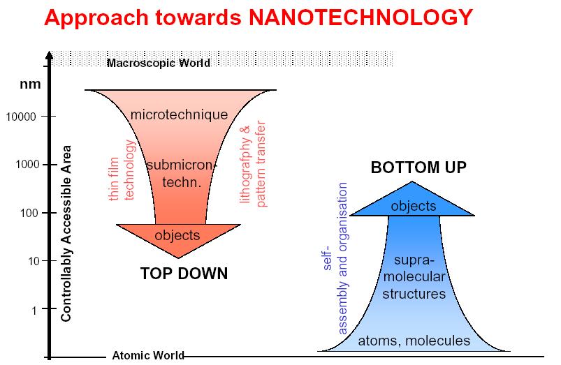
5 TECHNOLOGY?

. *V. Trabadelo et al.")
. *S. Merino et al.")
. *S. Merino et al.")
6 Thermal imprint lithography h r =h 0 -h pr ν *S. Merino et al. The Influence of Stamp deformation on Residual Layer Homogeneity in Thermal Nanoimprint Lithography. Microelectronic Engineering 85, 1892 (2008). *V. Trabadelo et al. Measurements of demolding forces in full wafer thermal nanoimprint. Microelectronic Engineering 85, 907 (2008). *S. Merino et al. The use of automatic demolding in NIL processes. Microelectronic Engineering 84, 958 (2007). *S. Merino et al. A new way of manufacturing high resolution optical encoders by NIL. Microelectronic Engineering 84, 848 (2007).

7 1) DNA detection by stretching in nanochannels The general idea behind the DNA stretching methods is to use nanofluidic channels to linearize double strands of DNA and read information. This information can be read either optically, by using fluorescent labels, or electrically, by including electrical probes inside the channels.
, composed by sequences of nucleotides, that is naturally coiled into a ball of several microns to fit inside the cell nucleus.")
8 DNA is a long chain polymer (0.34 nm/bp) naturally coiled into a ball (few microns). The DNA is a extremely long molecule (cm long), composed by sequences of nucleotides, that is naturally coiled into a ball of several microns to fit inside the cell nucleus. The current methods of analysing DNA requires chopping in shorter segments, replicating each segment a million times, sorting by size and piecing the original sequence back together in a time consuming and costly process. In contrast, Austin and Chou groups at Princeton developed the concept of stretching single molecules of DNA to analyse then.

9 Nanofluidic channels are currently being used for DNA stretching and direct visualization of the genomic length. This method provides important advantages such us rapid DNA restriction mapping in short times, reduction of the DNA sample down to single molecule genomic content, parallel analysis and more sensible detection. R g =(PwL 3 ) 1/5 bulk solution R g >>D>P L Z ( pw) L D 1 / 3 2 / nm/base pair 50, 100 and 200 nm line width and 80 nm in depth. Austin et al. The art of sucking spaghetti. Nature materials: 2; (2003) -Design and fabrication using NanoImprint Lithography of a nanofluidic device for DNA stretching applications. E. Abad et al. Microelectronic Engineering, 85, 818 (2008). -DNA analysis by single molecule stretching in nanofluidic biochips. E. Abad et al. Microelectronic Engineering ; 88, 300 (2011).
.")
10 *When D>P, the molecule is free to coil in the nanochannel and the elongation is due entirely to excluded volume interactions between segments of the polymer greatly separated in position along the backbone (fig. a). De Gennes theory developed a scaled argument for the average extension of a r L(wP/D 2 ) 1/3 confined self-avoiding polymer *When D<P, the physics is dominated not by excluded volume but by the interplay of confinement and intrinsic DNA elasticity. In the strong confinement limit D<<p, backfolding is energetically unfavourable and contour length is stored exclusively in deflections made by the polymer with the walls. These deflections occur on average over the Odijk scale λ (D 2 P) 1/3 and assuming that the average deflection made by the polymer with the walls is small, r= L[1-A(D/P) 2/3 ] (A 0.36). W. Reisner et al. Physical Reviews Letters 94, (2005). Log-log plot of the best power law fit


11 D 100nm Advantages of using micro/nanofluidics: Short reaction time Reduction of the DNA sample (ng->fg) Parallel analysis and high sensitivity Uniform stretching (no external force)

12 Chips manufacturing process Nanofluidic channels are currently being used for DNA stretching and direct visualization of the genomic length. This method provides important advantages such us rapid DNA restriction mapping in short times, reduction of the DNA sample down to single molecule genomic content, parallel analysis and more sensible detection.


13 Silicon stamp with post and channel-lines Top-view of the entry to the channel-lines Pattern transfer on silicon Cross-sections view of the nanochannels


14 Silicon-glass chip with electrodes defined in Pt on the pyrex. Top-view of the nanochannels through the glass (63X in oil. NA=1.4) Different packaging of the chip to introduce the DNA sample


15 Optical image of the filling of the device Filling with a fluorescent solution of rhodamine B Stretching of -DNA molecules(48502bp=16.5 m) in nanochannels. Fluorescent label YOYO-1 (1:5) nicking recoil
16 Histogram of the measured extension lengths of a single -DNA molecule. The average extension length, based on an analysis of 300 consecutive frames, is 5.8 m Extension factor: 0.3 Histogram of the measured average extension lengths of the complete set of -DNA molecules analyzed. The overall average extension obtained from a Gaussian fit of the peak is Lz = 6.0 m and the standard deviation is 0.3 m. The red lines show the Gaussian -DNA 48500pb => L=16.5 m y L dye (1:5)~ 20.5 m L ext L dye w P eff dye 2 D 1 3 D=130 nm The developed technology is a good alternative for the fabrication of biochips for single molecule DNA stretching applications


17 Guías nanofotónicas
18 2) Detección de DNA mediante detección electroquímica 1.Voltamperometría: corriente electroquímica generada por reacciones red/ox en los dígitos. 2. Espectroscopía de Impedancias: medida de la resisitividad y capacidad de la disolución en función de la frecuencia. V A Z ~ V


19 Fabricación de chips a escala micro y a escala nano

20 Detección de hibridación de DNA característico de escherichia coli -Electrodos comerciales/electrodos thin-films - Baja el LoD si electrodos interdigitados nano? - Fiabilidad de la medida?. Comparativa con métodos ópticos. Detección de proteínas y patógenos a través de la inmovilización de proteínas
 with functional group: succinimidil imide.")


- tetrahydrooctyl-trichlorosilane)")
21 3) BIOSENSORS FOR PROTEIN DETECTION Biofunctionalised PMMA copolymer (Tg=86ºC. Viscosity=6.7cp) with functional group: succinimidil imide. Covalent binding between succinimidil imide and amino group of proteins ELISA tests to check the differential affinity of protein adsorption between the copolymer and the antiadhesive layer coating Stablisment of optimal conditions Imprinting Demolding Residual layer etching F 13 -TCS Streptavidin protein adhesion Antiadhesive layer coating with F 13 -TCS (tridecafluoro-(1,1,2,2)- tetrahydrooctyl-trichlorosilane) developed. 114º
 micro (grating with 10 m period and equal line width and")


22 A fluorescence labeled streptavidin Alexa-Fluor 488 conjugated was put on the i) micro (grating with 10 m period and equal line width and space) and ii) nano (200 nm width lines spaced some micrometers) patterned areas of the surfaces. BIOSENSOR TO DETECT IgG Rabbit anti-igg with Alexa Fluor 488 Biotinilated rabbit anti-inmunoglobine antibody Threshold detection better than 200 ng/ml S. Merino et al. Protein patterning on the micro and nanoscale by thermal NIL on a new functionalized copolymer. Journal of Vacuum, Science and Technology B 27 (6), 2439 (2009).


23 Protein patterning by thermal nanoimprint lithography and plasma functionalization of polystyrene Selective binding of SAv to the activated surfaces is achieved by first binding a biotin linker with an activated carboxylic acid function to the formed amino groups. Binding tests were carried out with fluorescent labelled SAv. The fluorescence intensity was much higher in the plasma treated PS, while much less protein binding was found when the NH 3 plasma step was omitted. Non-exposed Exposed Biotin linker Presence of amino groups is confirmed
24 Fluorescence Intensity (a.u.) Sandwich-type immunoassay to detect the presence of the IgG protein on a sample Si SiO2 PS LC-sulfo-NHS- biotin Biotinylated antibody SAv Rabbit IgG Secondary antibody-alexa Fluor m IgG 50 g/ml 2,0 1,9 1,8 1,7 1,6 1,5 1,4 1,3 1,2 0,01 0, IgG concentration ( g/ml) The developed immunoassay was used to quantify the IgG content of several solutions, yielding a detection limit at about 50 ng/ml. V. Trabadelo et al. Protein patterning by thermal nanoimprint lithography and NH 3 plasma functionalization of polystyrene. Journal of Vacuum, Science and Technology B 27 (3), (2009).


25 Los SP son muy sensibles a cambios del índice de refracción en la vecindad de la superficie Hay que inmovilizar proteínas en oro.

26 1) Secondary antibody TNF antitnf amine coupling gold pg/ml Proteínas TNF-α e IL-6


27 Transmisión extraordinaria de luz a través de redes de nanoagujeros Fabricación de las redes mediante nanoimpresión y deposición de oro.
")

")


28 4) TISSUE ENGINEERING Morphological and biochemical changes of cells: (Tekniker-3B) Objective: To study how the interaction between topography and growth factors (cytokines) on the extracellular matrix (PLGA, PCL, natural polymers based on polysacharides) lead to morphological and biochemical changes in cells (fibroblasts, osteoblasts, human bone marrow stem cells). Pitch structures between 3 and 12 m 1.3 m 2.7 m 5 m 1.3 m 2.7 m 5 m Surface area Cell length


29 5 m 2.7 m 1.3 m
 Human bone marrow stem cells")


30 ALP conc. ( M) Human bone marrow stem cells aligned on structured hyaluronic acid substrates Strepatavidin and BSA proteins patterned on Hyaluronic acid substrates ALP quantification from hbmscs cultured on PLGA patterns under osteogenic differentiation conditions Alkalyne Phosphatase 7 days 14 days Blank and different patterned substrates

, in which the stochastic process such a diffusion is minor.")
 1/2 1. Separation of white blood cells, red blood cells and platelets from blood.")
31 5) Cells separation in blood. Use of microfluidic devices to separate cells attending its size. The separation technique is based on the concept of displacement lateral deterministic (DLD), in which the stochastic process such a diffusion is minor. =d/ =tg =1/N Under certain simplifications and with N large and h>>d c ; D c = 2G/N with =1/(3N) 1/2 1. Separation of white blood cells, red blood cells and platelets from blood. 2. Devices to enrich fetal cells from maternal blood, as a tool to perform a non-invasive prenatal diagnosis


32
 Organic Distributed Feedback Lasers - Pump")

 Pump intensity Active")

33 Outputintensity/ Arb. units 6) Organic Distributed Feedback Lasers - Pump (optical): pulsed Nd:YAG laser (10 ns, 10 Hz) operating at 532 nm. - Active medium: polystyrene doped with 0.5 wt% of a perylendiimide derivative (PDI). Amplified spontaneous emission (ASE) Pump intensity Active medium ASE Presence of ASE Stimulated emission I out 1,5 Is/40 Low pump High pump 1,0 Spontaneous Emission Estimulated Emission 0,5 IThreshold Ipump 0, Wavelength / nm
 operating at 532 nm.")
.")


34 Basic elements - Pump (optical): pulsed Nd:YAG laser (10 ns, 10 Hz) operating at 532 nm. - Active medium: polystyrene doped with 0.5 wt% of a perylendiimide derivative (PDI). - Resonator: distributed feedback (DFB) grating Bragg condition m Bragg = 2n eff m = 2 = 368 nm Light propagating in a waveguide mode is scattered from the periodic structure to create a diffracted wave propagating Pump intensity ~ 20º spot ~ 1 mm 2 DFB emission in some new direction.


35 PhC lasers are pumped vertically from above with a Q-switched frequency doubled neodynium doped aluminium yttrium garnet laser at 532 nm
36 Most remarkable properties Lasing threshold Photostability Without resonator 2.5 J p -1 V. Trabadelo et al., Microelectron. Eng., 87, 1428 (2010) V. Navarro-Fuster et al., Appl. Phys. Lett. 97, (2010) Photoestability halflife 1/2 : 3 x 10 5 pulses (10 ns, 4 J p -1 ) at 10 Hz
 at 533 nm. *Threshold: 3 µj/pulse 0,6 0,4 Red3 *Photostability: more than 100.000 pulses (i.e. 3h at 10 Hz) with pumping energy at 6 µj/pulse 0,2 Red1 0,0 566 568 570 572 574 Wavelength/ nm")
37 Emitted Intensity/ a.u. red h = 368 nm. h= 340 nm. = 368 nm. h= 220 nm. = 368 nm. h= 105 nm. 1,2 1,0 0,8 DFB2 = 569,7 nm DFB3 = 570,3 nm DFB1 = 569,7 nm Red2 *Pump: Nd:Yag (10 ns, 10 Hz) at 533 nm. *Threshold: 3 µj/pulse 0,6 0,4 Red3 *Photostability: more than pulses (i.e. 3h at 10 Hz) with pumping energy at 6 µj/pulse 0,2 Red1 0, Wavelength/ nm
 : waveguide of thickness h+(d/2) (grating depth =")
38 Last results: Wavelength tunability SiO2 gratings Model h : waveguide of thickness h Model h+(d/2) : waveguide of thickness h+(d/2) (grating depth = 220 nm)
39 Last results: Wavelength tunability gratings on doped PS h d Model h : waveguide of thickness h Model h+(d/2) : waveguide of thickness h+(d/2) (grating depth = 220 nm)
40 2D structures to reduce threshold of laser emission.

41 Follow-up i) Use of polymer-semiconductor nanocomposites based on IV-VI nanopaticles emitting in the NIR region: CdHgTe, PbS, PbSe. ii) DFB Biosensors
In-Situ Monitoring of Pattern Filling in Nano-Imprint Lithography Using Surface Plasmon Resonance
 Copyright 2011 American Scientific Publishers All rights reserved Printed in the United States of America Journal of Nanoscience and Nanotechnology Vol. 11, 1 6, 2011 In-Situ Monitoring of Pattern Filling
Nanophotonics: principle and application. Khai Q. Le Lecture 11 Optical biosensors
 Nanophotonics: principle and application Khai Q. Le Lecture 11 Optical biosensors Outline Biosensors: Introduction Optical Biosensors Label-Free Biosensor: Ringresonator Theory Measurements: Bulk sensing
Vertically aligned Ni magnetic nanowires fabricated by diblock-copolymer-directed Al thin film anodization
 Vertically aligned Ni magnetic nanowires fabricated by diblock-copolymer-directed Al thin film anodization Researcher: Kunbae (Kevin) Noh, Graduate Student, MAE Dept. and CMRR Collaborators: Leon Chen,
Excimer Laser Annealing of Hydrogen Modulation Doped a-si Film
 Materials Transactions, Vol. 48, No. 5 (27) pp. 975 to 979 #27 The Japan Institute of Metals Excimer Laser Annealing of Hydrogen Modulation Doped a-si Film Akira Heya 1, Naoto Matsuo 1, Tadashi Serikawa
Multiphoton lithography based 3D micro/nano printing Dr Qin Hu
 Multiphoton lithography based 3D micro/nano printing Dr Qin Hu EPSRC Centre for Innovative Manufacturing in Additive Manufacturing University of Nottingham Multiphoton lithography Also known as direct
Metallization deposition and etching. Material mainly taken from Campbell, UCCS
 Metallization deposition and etching Material mainly taken from Campbell, UCCS Application Metallization is back-end processing Metals used are aluminum and copper Mainly involves deposition and etching,
Nanostructure Fabrication by Nanoimprint Lithography and its Applications
 Nanostructure Fabrication by Nanoimprint Lithography and its Applications Those slides summarized several research projects I carried out at National Research Council (NRC) during 2003-2008 Bo Cui CNRC-Industrial
Procese de depunere in sistemul Plasma Enhanced Chemical Vapor Deposition (PECVD)
") Procese de depunere in sistemul Plasma Enhanced Chemical Vapor Deposition (PECVD) Ciprian Iliescu Conţinutul acestui material nu reprezintă in mod obligatoriu poziţia oficială a Uniunii Europene sau a
Procese de depunere in sistemul Plasma Enhanced Chemical Vapor Deposition (PECVD) Ciprian Iliescu Conţinutul acestui material nu reprezintă in mod obligatoriu poziţia oficială a Uniunii Europene sau a
THIN FILM THICKNESS MEASUREMENT FOR EVALUATION OF RESIDUAL LAYER OF NANO-IMPRINT LITHOGRAPHY USING NEAR-FIELD OPTICS
 9 th INTERNATIONAL SYMPOSIUM ON MEASUREMENT AND QUALITY CONTROL (9 th ISMQC) November 21 24, 27, IIT Madras THIN FILM THICKNESS MEASUREMENT FOR EVALUATION OF RESIDUAL LAYER OF NANO-IMPRINT LITHOGRAPHY
Superionic Solid State Stamping (S4)
") Superionic Solid State Stamping (S4) Lead Faculty Researcher: Placid Ferreira Department: Materials Science & Engineering Hsu et al, Nano Letters, 2007 1. Description: This dry, single step, electrochemical
Superionic Solid State Stamping (S4) Lead Faculty Researcher: Placid Ferreira Department: Materials Science & Engineering Hsu et al, Nano Letters, 2007 1. Description: This dry, single step, electrochemical
Innovative sensors and systems for the molecular Point-of-Care diagnostics
 Innovative sensors and systems for the molecular Point-of-Care diagnostics AIT Austrian Institute of Technology GmbH Health & Environment Department Molecular Diagnostics Contact Giorgio.Mutinati@ait.ac.at
Simple method for formation of nanometer scale holes in membranes. E. O. Lawrence Berkeley National Laboratory, Berkeley, CA 94720
 Simple method for formation of nanometer scale holes in membranes T. Schenkel 1, E. A. Stach, V. Radmilovic, S.-J. Park, and A. Persaud E. O. Lawrence Berkeley National Laboratory, Berkeley, CA 94720 When
MICROFABRICATION OF OPTICALLY ACTIVE InO X MICROSTRUCTURES BY ULTRASHORT LASER PULSES
 Journal of Optoelectronics and Advanced Materials Vol. 4, No. 3, September 2002, p. 809-812 MICROFABRICATION OF OPTICALLY ACTIVE InO X MICROSTRUCTURES BY ULTRASHORT LASER PULSES Foundation for Research
Integration of Block-Copolymer with Nano- Imprint Lithography: Pushing the Boundaries of Emerging Nano-Patterning Technology
 Integration of Block-Copolymer with Nano- Imprint Lithography: Pushing the Boundaries of Emerging Nano-Patterning Technology April 2010 update SNL Geoff Brennecka (PI) Bruce Burckel Matt George Jack Skinner
CREOL, The College of Optics & Photonics, University of Central Florida
 Metal Substrate Induced Control of Ag Nanoparticle Plasmon Resonances for Tunable SERS Substrates Pieter G. Kik 1, Amitabh Ghoshal 1, Manuel Marquez 2 and Min Hu 1 1 CREOL, The College of Optics and Photonics,
ADOPT Winter School Merging silicon photonics and plasmonics
 ADOPT Winter School 2014 Merging silicon photonics and plasmonics Prof. Min Qiu Optics and Photonics, Royal Institute of Technology, Sweden and Optical Engineering, Zhejiang University, China Contents
Combinatorial RF Magnetron Sputtering for Rapid Materials Discovery: Methodology and Applications
 Combinatorial RF Magnetron Sputtering for Rapid Materials Discovery: Methodology and Applications Philip D. Rack,, Jason D. Fowlkes, and Yuepeng Deng Department of Materials Science and Engineering University
Nanotechnological Applications of Biomolecular Motor Systems. Stefan Diez Max-Planck-Institute of Molecular Cell Biology and Genetics Dresden
 Nanotechnological Applications of Biomolecular Motor Systems Stefan Diez Max-Planck-Institute of Molecular Cell Biology and Genetics Dresden Max-Planck-Institute of Molecular Cell Biology and Genetics
OLED/OPD transducer for point-of-use diagnostics
 OLED/OPD transducer for point-of-use diagnostics Overview 1. CDT overview + Biosensor platform overview CDT overview Absorbance based lateral flow device (LFD) basics and advantages Abingdon Health collaboration
PeakForce Tapping and ScanAsyst An introduction to the technique featuring Bruker s Dimension Edge. Bede Pittenger, Ph.D.
 PeakForce Tapping and ScanAsyst An introduction to the technique featuring Bruker s Dimension Edge Bede Pittenger, Ph.D. Dimension Edge with ScanAsyst: High performance AFM breaking down cost and productivity
Ajay Kumar Gautam [VLSI TECHNOLOGY] VLSI Technology for 3RD Year ECE/EEE Uttarakhand Technical University
![Ajay Kumar Gautam [VLSI TECHNOLOGY] VLSI Technology for 3RD Year ECE/EEE Uttarakhand Technical University](/thumbs/75/72824557.jpg "Ajay Kumar Gautam [VLSI TECHNOLOGY] VLSI Technology for 3RD Year ECE/EEE Uttarakhand Technical University") 2014 Ajay Kumar Gautam [VLSI TECHNOLOGY] VLSI Technology for 3RD Year ECE/EEE Uttarakhand Technical University Page1 Syllabus UNIT 1 Introduction to VLSI Technology: Classification of ICs, Scale of integration,
2014 Ajay Kumar Gautam [VLSI TECHNOLOGY] VLSI Technology for 3RD Year ECE/EEE Uttarakhand Technical University Page1 Syllabus UNIT 1 Introduction to VLSI Technology: Classification of ICs, Scale of integration,
Processing guidelines
 Processing guidelines mr-uvcur21 series UV-curable Polymer for UV-based Nanoimprint Lithography Characteristics mr-uvcur21 is a liquid UV-curable polymer system with low viscosity and high curing rate
PARAMETER EFFECTS FOR THE GROWTH OF THIN POROUS ANODIC ALUMINUM OXIDES
 10.1149/1.2794473, The Electrochemical Society PARAMETER EFFECTS FOR THE GROWTH OF THIN POROUS ANODIC ALUMINUM OXIDES S. Yim a, C. Bonhôte b, J. Lille b, and T. Wu b a Dept. of Chem. and Mat. Engr., San
X-ray Photoelectron Spectroscopy
 X-ray Photoelectron Spectroscopy X-ray photoelectron spectroscopy (XPS) is a non-destructive technique used to analyze the elemental compositions, chemical and electronic states of materials. XPS has a
Micro and nano structuring of carbon based materials for micro injection moulding and hot embossing
 Micro and nano structuring of carbon based materials for micro injection moulding and hot embossing Victor Usov, Graham Cross, Neal O Hara, Declan Scanlan, Sander Paulen, Chris de Ruijter, Daniel Vlasveld,
Micro-Electro-Mechanical Systems (MEMS) Fabrication. Special Process Modules for MEMS. Principle of Sensing and Actuation
 Fabrication. Special Process Modules for MEMS. Principle of Sensing and Actuation") Micro-Electro-Mechanical Systems (MEMS) Fabrication Fabrication Considerations Stress-Strain, Thin-film Stress, Stiction Special Process Modules for MEMS Bonding, Cavity Sealing, Deep RIE, Spatial forming
Micro-Electro-Mechanical Systems (MEMS) Fabrication Fabrication Considerations Stress-Strain, Thin-film Stress, Stiction Special Process Modules for MEMS Bonding, Cavity Sealing, Deep RIE, Spatial forming
Nanobiotechnology. Place: IOP 1 st Meeting Room Time: 9:30-12:00. Reference: Review Papers. Grade: 50% midterm, 50% final.
 Nanobiotechnology Place: IOP 1 st Meeting Room Time: 9:30-12:00 Reference: Review Papers Grade: 50% midterm, 50% final Midterm: 5/15 History Atom Earth, Air, Water Fire SEM: 20-40 nm Silver 66.2% Gold
Surface Micromachining
 Surface Micromachining Outline Introduction Material often used in surface micromachining Material selection criteria in surface micromachining Case study: Fabrication of electrostatic motor Major issues
TSV Processing and Wafer Stacking. Kathy Cook and Maggie Zoberbier, 3D Business Development
 TSV Processing and Wafer Stacking Kathy Cook and Maggie Zoberbier, 3D Business Development Outline Why 3D Integration? TSV Process Variations Lithography Process Results Stacking Technology Wafer Bonding
2.1 µm CW Raman Laser in GeO 2 Fiber
 2.1 µm CW Raman Laser in GeO 2 Fiber B. A. Cumberland, S. V. Popov and J. R. Taylor Femtosecond Optics Group, Imperial College London, SW7 2AZ, United Kingdom O. I. Medvedkov, S. A. Vasiliev, E. M. Dianov
High Power Operation of Cryogenic Yb:YAG. K. F. Wall, B. Pati, and P. F. Moulton Photonics West 2007 San Jose, CA January 23, 2007
 High Power Operation of Cryogenic Yb:YAG K. F. Wall, B. Pati, and P. F. Moulton Photonics West 2007 San Jose, CA January 23, 2007 Outline Early work on cryogenic lasers MPS laser technology Recent program
Light enhancement by the formation of an Al-oxide honeycomb nano-structure on the n-gan surface of thin-gan light-emitting diodes
 Light enhancement by the formation of an Al-oxide honeycomb nano-structure on the n-gan surface of thin-gan light-emitting diodes C. L. Lin, P. H. Chen Department of Chemical and Materials Engineering,
R Sensor resistance (Ω) ρ Specific resistivity of bulk Silicon (Ω cm) d Diameter of measuring point (cm)
 ρ Specific resistivity of bulk Silicon (Ω cm) d Diameter of measuring point (cm)") 4 Silicon Temperature Sensors 4.1 Introduction The KTY temperature sensor developed by Infineon Technologies is based on the principle of the Spreading Resistance. The expression Spreading Resistance derives
4 Silicon Temperature Sensors 4.1 Introduction The KTY temperature sensor developed by Infineon Technologies is based on the principle of the Spreading Resistance. The expression Spreading Resistance derives
Characterization of Materials with a Combined AFM/Raman Microscope
 Characterization of Materials with a Combined AFM/Raman Microscope Marko Surtchev 1, Sergei Magonov 1 and Mark Wall 2 1 NT-MDT America, Tempe, AZ U.S.A. 2 Thermo Fisher Scientific, Madison, WI, U.S.A.
Introduction of Biosensors
 Introduction of Biosensors Lecture April 17 Jeff T.H.Wang website: http://pegasus.me.jhu.edu/~thwang/ New course : BioMEMS and BioSensing (Spring 04 ) What s is a biosensor? Target 4.22 Signal Signal Analtye
Procedure to deposit Gold only on the sidewalls of rectangular nanostructures and its applications
 Procedure to deposit Gold only on the sidewalls of rectangular nanostructures and its applications Zain Zaidi, Saara Khan, James Conway, J Provine, Michelle Rincon, Roger Howe Stanford University, USA
Ultra High Barrier Coatings by PECVD
 Society of Vacuum Coaters 2014 Technical Conference Presentation Ultra High Barrier Coatings by PECVD John Madocks & Phong Ngo, General Plasma Inc., 546 E. 25 th Street, Tucson, Arizona, USA Abstract Silicon
Label-Enhanced SPR Improves the Detectability of Label-Free Surface Plasmon Resonance Analysis 100x
 episentec Label-Enhanced SPR Improves the Detectability of Label-Free Surface Plasmon Resonance Analysis 1x Anders Hanning, Episentec Drug Discovery 15, Telford, 2-3 September 215 Episentec - Better Biosensors
Nanofabrication Prof. Stephen Y. Chou NanoStructure Laboratory
 Nanofabrication Prof. Stephen Y. Chou Department of Electrical Engineering Princeton University 1 Acknowledgment Dr. Paul Fischer Dr. Yun Wang Dr. Jay Guo Dr. Peter Klauss Dr. Jim Wang Dr. Longtin He Dr.
Photolithography I ( Part 2 )
") 1 Photolithography I ( Part 2 ) Chapter 13 : Semiconductor Manufacturing Technology by M. Quirk & J. Serda Bjørn-Ove Fimland, Department of Electronics and Telecommunication, Norwegian University of Science
1 Photolithography I ( Part 2 ) Chapter 13 : Semiconductor Manufacturing Technology by M. Quirk & J. Serda Bjørn-Ove Fimland, Department of Electronics and Telecommunication, Norwegian University of Science
Structure and optical properties of M/ZnO (M=Au, Cu, Pt) nanocomposites
 nanocomposites") Solar Energy Materials & Solar Cells 8 () 339 38 Structure and optical properties of M/ (M=Au, Cu, Pt) nanocomposites U. Pal a,b, *, J. Garc!ıa-Serrano a, G. Casarrubias-Segura a, N. Koshizaki c, T. Sasaki
Solar Energy Materials & Solar Cells 8 () 339 38 Structure and optical properties of M/ (M=Au, Cu, Pt) nanocomposites U. Pal a,b, *, J. Garc!ıa-Serrano a, G. Casarrubias-Segura a, N. Koshizaki c, T. Sasaki
Analysis of optical properties of solar energy materials
 Analysis of optical properties of solar energy materials Comices Energie solaire - Namur - 23/04/2012 Michel Voué Physique des Matériaux et Optique Centre de Recherche en Physique des Matériaux Université
FABRICATION PROCESSES FOR MAGNETIC MICROACTUATORS WITH POLYSILICON FLEXURES. Jack W. Judy and Richard S. Muller
 FABRICATION PROCESSES FOR MAGNETIC MICROACTUATORS WITH POLYSILICON FLEXURES Jack W. Judy and Richard S. Muller Berkeley Sensor & Actuator Center (BSAC) Department of EECS, University of California, Berkeley,
Towards scalable fabrication of high efficiency polymer solar cells
 Towards scalable fabrication of high efficiency polymer solar cells Hui Joon Park 2*, Myung-Gyu Kang 1**, Se Hyun Ahn 3, Moon Kyu Kang 1, and L. Jay Guo 1,2,3 1 Department of Electrical Engineering and
LOT. Contents. Introduction to Thin Film Technology. Chair of Surface and Materials Technology
 Introduction to Thin Film Contents 1. Introduction and Application Examples (2h) 2. Preparation of Thin Films by PVD (Physical Vapor Deposition) (6h) 2.1 Vacuum Technique (1h) 2.1.1 Kinetics of Gases 2.1.2
350 C for 8 hours in argon atmosphere. Supplementary Figures. Supplementary Figure 1 High-temperature annealing of BP flakes on SiO 2.
 Supplementary Figures Supplementary Figure 1 High-temperature annealing of BP flakes on SiO 2. (a-d) The optical images of three BP flakes on a SiO 2 substrate before (a,b) and after annealing (c,d) at
Silicon photonics biosensing: different packaging platforms and applications ABSTRACT 1. REACTION TUBES AS A PLATFORM FOR RING RESONATOR SENSORS.
 Silicon photonics biosensing: different packaging platforms and applications C. Lerma Arce a,b, E. Hallynck a,b, S. Werquin a,b, J.W. Hoste a,b, D. Martens a,b, P. Bienstman a,b,* a Photonics Research
Free standing Multilayer Thin Film of Cellulose Nanocrystals
 Free standing Multilayer Thin Film of Cellulose Nanocrystals Chaoyang Jiang Department of Chemistry The University of South Dakota Edmonton, June 25, 2009 Cellulose Nanocrystals Nanotechnology R&D Priority
Laser printing and curing/sintering of silver paste lines for solar cell metallization
 Lasers in Manufacturing Conference 2015 Laser printing and curing/sintering of silver paste lines for solar cell metallization D. Munoz-Martin a *, Y. Chen a, A. Márquez a, M. Morales a, C. Molpeceres
Visualization and Control of Particulate Contamination Phenomena in a Plasma Enhanced CVD Reactor
 Visualization and Control of Particulate Contamination Phenomena in a Plasma Enhanced CVD Reactor Manabu Shimada, 1 Kikuo Okuyama, 1 Yutaka Hayashi, 1 Heru Setyawan, 2 and Nobuki Kashihara 2 1 Department
Supplementary Figure 1 Scanning electron micrograph (SEM) of a groove-structured silicon substrate. The micropillars are ca. 10 μm wide, 20 μm high
 of a groove-structured silicon substrate. The micropillars are ca. 10 μm wide, 20 μm high") Supplementary Figure 1 Scanning electron micrograph (SEM) of a groove-structured silicon substrate. The micropillars are ca. 10 μm wide, 20 μm high and own the gap of 10 μm. Supplementary Figure 2 Strictly
Supplementary Figure 1 Scanning electron micrograph (SEM) of a groove-structured silicon substrate. The micropillars are ca. 10 μm wide, 20 μm high and own the gap of 10 μm. Supplementary Figure 2 Strictly
Plasmonic Nanostructures II
 Plasmonic Nanostructures II Dr. Krüger / Prof. M. Zacharias, IMTEK, Propagation of SPPs Propagation distance decreases with decreasing strip width! 2 Dr. Krüger / Prof. M. Zacharias, IMTEK, Bound and leaky
Modification of Glass by FS Laser for Optical/Memory Applications
 Modification of Glass by FS Laser for Optical/Memory Applications Kazuyuki Hirao and Kiyotaka Miura Department of Material Chemistry Kyoto University International Workshop on Scientific Challenges of
Surface micromachining and Process flow part 1
 Surface micromachining and Process flow part 1 Identify the basic steps of a generic surface micromachining process Identify the critical requirements needed to create a MEMS using surface micromachining
How to run Alpha assay: How to setup an Alpha assay Make your own assay!
 How to run Alpha assay: How to setup an Alpha assay Make your own assay! 1 2009 PerkinElmer AlphaLISA kits - recommendations before starting the assay Samples: Phenol red and hemoglobin: choose AlphaLISA
Supporting Information
 Supporting Information Fast-Response, Sensitivitive and Low-Powered Chemosensors by Fusing Nanostructured Porous Thin Film and IDEs-Microheater Chip Zhengfei Dai,, Lei Xu,#,, Guotao Duan *,, Tie Li *,,
Laser damage threshold of AR coatings on phosphate glass
 Laser damage threshold of AR coatings on phosphate glass Optical Coatings for Laser Applications Wednesday, 12 th April 2017, Buchs SG, Switzerland dirk.apitz@schott.com, SCHOTT Suisse SA, Advanced Optics,
SURFACE PLASMON RESONANCE-BASED SYSTEMS
 SURFACE PLASMON RESONANCE-BASED SYSTEMS ADVANCED METHODS IN BIOENGINEERING LABORATORY 3/1/2011 1 Schedule Week 1: Introduction Reagents preparation Ligand immobilization of Protocol 1 Week 2: Kinetics
Anomaly of Film Porosity Dependence on Deposition Rate
 Anomaly of Film Porosity Dependence on Deposition Rate Stephen P. Stagon and Hanchen Huang* Department of Mechanical Engineering, University of Connecticut, Storrs, CT 06269 J. Kevin Baldwin and Amit Misra
Lecture 12. Physical Vapor Deposition: Evaporation and Sputtering Reading: Chapter 12. ECE Dr. Alan Doolittle
 Lecture 12 Physical Vapor Deposition: Evaporation and Sputtering Reading: Chapter 12 Evaporation and Sputtering (Metalization) Evaporation For all devices, there is a need to go from semiconductor to metal.
Coatings. Ion Assisted Deposition (IAD) process Advance Plasma Source (APS) plasma-ion assisted Deposition. Coatings on Optical Fibers
 process Advance Plasma Source (APS) plasma-ion assisted Deposition. Coatings on Optical Fibers") Anti-Reflection Custom Ion Assisted Deposition (IAD) process Advance Plasma Source (APS) plasma-ion assisted Deposition Anti-Reflection on Optical Fibers OptoSigma supplies a wide selection of optical
Anti-Reflection Custom Ion Assisted Deposition (IAD) process Advance Plasma Source (APS) plasma-ion assisted Deposition Anti-Reflection on Optical Fibers OptoSigma supplies a wide selection of optical
Visit
 Practical Applications for Nano- Electronics by Vimal Gopee E-mail: Vimal.gopee@npl.co.uk 10/10/12 Your Delegate Webinar Control Panel Open and close your panel Full screen view Raise hand for Q&A at the
BONDING OF MULTIPLE WAFERS FOR HIGH THROUGHPUT LED PRODUCTION. S. Sood and A. Wong
 10.1149/1.2982882 The Electrochemical Society BONDING OF MULTIPLE WAFERS FOR HIGH THROUGHPUT LED PRODUCTION S. Sood and A. Wong Wafer Bonder Division, SUSS MicroTec Inc., 228 SUSS Drive, Waterbury Center,
Growth Of TiO 2 Films By RF Magnetron Sputtering Studies On The Structural And Optical Properties
 Journal of Multidisciplinary Engineering Science and Technology (JMEST) Growth Of TiO 2 Films By RF Magnetron Sputtering Studies On The Structural And Optical Properties Ahmed K. Abbas 1, Mohammed K. Khalaf
R&D ACTIVITIES AT ASSCP-BHEL,GURGAON IN SOLAR PV. DST-EPSRC Workshop on Solar Energy Research
 R&D ACTIVITIES AT -BHEL,GURGAON IN SOLAR PV at the DST-EPSRC Workshop on Solar Energy Research (22 nd 23 rd April, 2009) by Dr.R.K. Bhogra, Addl. General Manager & Head Email: cpdrkb@bhel.co.in Dr.A.K.
Neodymium Doped Yttrium Orthovanadate (Nd:YVO4)
") Neodymium Doped Yttrium Orthovanadate (Nd:YVO4) Nd:YVO4 is the most efficient laser host crystal for diode pumping among the current commercial laser crystals, especially, for low to middle power density.
Neodymium Doped Yttrium Orthovanadate (Nd:YVO4) Nd:YVO4 is the most efficient laser host crystal for diode pumping among the current commercial laser crystals, especially, for low to middle power density.
Imagerie et spectroscopie de fluorescence par excitation non radiative
 Imagerie et spectroscopie de fluorescence par excitation non radiative comment s affranchir de la limite de diffraction Rodolphe Jaffiol, Cyrille Vézy, Marcelina Cardoso Dos Santos LNIO, UTT, Troyes NanoBioPhotonics
ME 189 Microsystems Design and Manufacture. Chapter 9. Micromanufacturing
 ME 189 Microsystems Design and Manufacture Chapter 9 Micromanufacturing This chapter will offer an overview of the application of the various fabrication techniques described in Chapter 8 in the manufacturing
Fs- Using Ultrafast Lasers to Add New Functionality to Glass
 An IMI Video Reproduction of Invited Lectures from the 17th University Glass Conference Fs- Using Ultrafast Lasers to Add New Functionality to Glass Denise M. Krol University of California, Davis 17th
Methods of Biomaterials Testing Lesson 3-5. Biochemical Methods - Molecular Biology -
 Methods of Biomaterials Testing Lesson 3-5 Biochemical Methods - Molecular Biology - Chromosomes in the Cell Nucleus DNA in the Chromosome Deoxyribonucleic Acid (DNA) DNA has double-helix structure The
Electron microscopy technology of reticulocytes after sorting with
 Electron microscopy technology of reticulocytes after sorting with magnetic beads The Cell Analysis Center Scientific Bulletin Part 2 For efficient analysis of cells, sorting of the target cells is crucial.
FABRICATION AND CHARACTERIZATION OF QUANTUM-WELL AND QUANTUM-DOT METAL CAVITY SURFACE-EMITTING NANOLASERS
 FABRICATION AND CHARACTERIZATION OF QUANTUM-WELL AND QUANTUM-DOT METAL CAVITY SURFACE-EMITTING NANOLASERS By Eric Wei Senior Thesis in Electrical Engineering University of Illinois at Urbana-Champaign
Repetition: Adhesion Mechanisms
 Repetition: Adhesion Mechanisms a) Mechanical interlocking b) Monolayer/monolayer c) Chemical bonding d) Diffusion e) Psedo diffusion due to augmented energy input (hyperthermal particles) Repetition:
LOW TEMPERATURE PHOTONIC SINTERING FOR PRINTED ELECTRONICS. Dr. Saad Ahmed XENON Corporation November 19, 2015
 LOW TEMPERATURE PHOTONIC SINTERING FOR PRINTED ELECTRONICS Dr. Saad Ahmed XENON Corporation November 19, 2015 Topics Introduction to Pulsed Light Photonic sintering for Printed Electronics R&D Tools for
Transmission Mode Photocathodes Covering the Spectral Range
 Transmission Mode Photocathodes Covering the Spectral Range 6/19/2002 New Developments in Photodetection 3 rd Beaune Conference June 17-21, 2002 Arlynn Smith, Keith Passmore, Roger Sillmon, Rudy Benz ITT
Vacuum casting, a new answer for manufacturing biomicrosystems
 1 Vacuum casting, a new answer for manufacturing biomicrosystems M Denoual 1 *, P Mognol 2, and B Lepioufle 1 1 Biomis-SATIE ENS-Cachan antenne de Bretagne, Bruz, France 2 IRCCyN Nantes, France The manuscript
Final Year Project Proposal 1
 Final Year Project Proposal 1 Mechanical testing for high temperature polymers Mr Eric Phua Jian Rong (JRPhua@ntu.edu.sg) In offshore subsea drilling, different types of microelectronics devices and sensors
Characterization of Aptamer Binding using SensíQ SPR Platforms
 Characterization of Aptamer Binding using SensíQ SPR Platforms APPLICATION NOTE INTRODUCTION Aptamers have the potential to provide a better solution in diagnostics and other research areas than traditional
EXCIMER LASER ANNEALING FOR LOW- TEMPERATURE POLYSILICON THIN FILM TRANSISTOR FABRICATION ON PLASTIC SUBSTRATES
 EXCIMER LASER ANNEALING FOR LOW- TEMPERATURE POLYSILICON THIN FILM TRANSISTOR FABRICATION ON PLASTIC SUBSTRATES G. Fortunato, A. Pecora, L. Maiolo, M. Cuscunà, D. Simeone, A. Minotti, and L. Mariucci CNR-IMM,
11.3 Polishing with Laser Radiation
 196 E. Willenborg 11.3 Polishing with Laser Radiation Edgar Willenborg The surface roughness of a part or product strongly influences its properties and functions. Among these can be counted abrasion and
Novel Microfluidic Valving and Packaging Designs for Protein Containing Biochips
 Novel Microfluidic Valving and Packaging Designs for Protein Containing Biochips Chunmeng Lu and L. James Lee Department of Chemical and Biomolecular Engineering The Ohio State University Lab-on on-a-chip
Process steps for Field Emitter devices built on Silicon wafers And 3D Photovoltaics on Silicon wafers
 Process steps for Field Emitter devices built on Silicon wafers And 3D Photovoltaics on Silicon wafers David W. Stollberg, Ph.D., P.E. Research Engineer and Adjunct Faculty GTRI_B-1 Field Emitters GTRI_B-2
Enabling Technology in Thin Wafer Dicing
 Enabling Technology in Thin Wafer Dicing Jeroen van Borkulo, Rogier Evertsen, Rene Hendriks, ALSI, platinawerf 2G, 6641TL Beuningen Netherlands Abstract Driven by IC packaging and performance requirements,
Regents of the University of California
 Surface-Micromachining Process Flow Photoresist Sacrificial Oxide Structural Polysilcon Deposit sacrificial PSG: Target = 2 m 1 hr. 40 min. LPCVD @450 o C Densify the PSG Anneal @950 o C for 30 min. Lithography
Step and Flash Imprint Lithography for sub-100nm Patterning
 Step and Flash Imprint Lithography for sub-100nm Patterning Matthew Colburn, Annette Grot, Marie Amistoso, Byung Jin Choi, Todd Bailey, John Ekerdt, S.V. Sreenivasan, James Hollenhorst, C. Grant Willson
MSD GOLD Streptavidin and Avidin Plates
 MSD GOLD Streptavidin and Avidin Plates SECTOR Plates QUICKPLEX Plates 96-well Streptavidin L15SA L55SA 96-well Small Spot Streptavidin L45SA N/A 96-well High Bind Avidin L15AB L55AB FOR RESEARCH USE ONLY.
Transmission Electron Microscopy (TEM) Prof.Dr.Figen KAYA
 Prof.Dr.Figen KAYA") Transmission Electron Microscopy (TEM) Prof.Dr.Figen KAYA Transmission Electron Microscope A transmission electron microscope, similar to a transmission light microscope, has the following components along
Transmission Electron Microscopy (TEM) Prof.Dr.Figen KAYA Transmission Electron Microscope A transmission electron microscope, similar to a transmission light microscope, has the following components along
The growth of patterned ceramic thin films from polymer precursor solutions Göbel, Ole
 University of Groningen The growth of patterned ceramic thin films from polymer precursor solutions Göbel, Ole IMPORTANT NOTE: You are advised to consult the publisher's version (publisher's PDF) if you
Metallic Antireflection Structures Made from Silver Ink by a Liquid Transfer Imprint Lithography Technique
 Journal of Photopolymer Science and Technology Volume 30, Number 5 (2017) 539-544 C 2017SPST Metallic Antireflection Structures Made from Silver Ink by a Liquid Transfer Imprint Lithography Technique Ichiro
VLSI Technology. By: Ajay Kumar Gautam
 By: Ajay Kumar Gautam Introduction to VLSI Technology, Crystal Growth, Oxidation, Epitaxial Process, Diffusion Process, Ion Implantation, Lithography, Etching, Metallization, VLSI Process Integration,
Magnetic Force Microscopy: nanoscale magnetic imaging and lithography
 NTEGRA Aura Magnetic Force Microscopy: nanoscale magnetic imaging and lithography The principle of Magnetic Force Microscopy (MFM) is based on the detection of the interaction between the sample and a
Gaetano L Episcopo. Introduction to MEMS
 Gaetano L Episcopo Introduction to MEMS What are MEMS? Micro Electro Mechanichal Systems MEMS are integrated devices, or systems of devices, with microscopic parts, such as: Mechanical Parts Electrical
SEPARATING PLASMA AND BLOOD CELLS BY DIELECTROPHORESIS IN MICROFLUIDIC CHIPS
 Fourth International Symposium on Physics of Fluids (ISPF4) International Journal of Modern Physics: Conference Series Vol. 19 (2012) 185 189 World Scientific Publishing Company DOI: 10.1142/S2010194512008732
1. Introduction. What is implantation? Advantages
 Ion implantation Contents 1. Introduction 2. Ion range 3. implantation profiles 4. ion channeling 5. ion implantation-induced damage 6. annealing behavior of the damage 7. process consideration 8. comparison
Antimicrobial Surfaces: Physical and Chemical Functionalization
 Antimicrobial Surfaces: Physical and Chemical Functionalization Iban Quintana EIBAR, May 3 th 2017 IK4-TEKNIKER 2017 Antimicrobial Surfaces Overview Passive Approach: Anti-biofouling Bactericidal Active
Ultra Fine Pitch Bumping Using e-ni/au and Sn Lift-Off Processes
 Ultra Fine Pitch Bumping Using e-ni/au and Sn Lift-Off Processes Andrew Strandjord, Thorsten Teutsch, and Jing Li Pac Tech USA Packaging Technologies, Inc. Santa Clara, CA USA 95050 Thomas Oppert, and
EE40 Lec 22. IC Fabrication Technology. Prof. Nathan Cheung 11/19/2009
 Suggested Reading EE40 Lec 22 IC Fabrication Technology Prof. Nathan Cheung 11/19/2009 300mm Fab Tour http://www-03.ibm.com/technology/manufacturing/technology_tour_300mm_foundry.html Overview of IC Technology
Positive Photoresists
 Positive Photoresists Gesellschaft für chemische Materialien spezieller Photoresistsysteme mbh Positive Photoresists map 1200 series Thick resists map 1275, map 1275 HV Unique features of the positive
RayBio Human bfgf ELISA Kit
 RayBio Human bfgf ELISA Kit User Manual (for Cell Lysate and Tissue Lysate) (Revised Mar 1, 2012) RayBio Human bfgf ELISA Kit Protocol (Cat#: ELH-bFGF-001C) RayBiotech, Inc. We Provide You With Excellent
Piezoelectric Polycrystalline (PZT) Components and Wafers
 Components and Wafers") Piezoelectric Polycrystalline (PZT) Components and Wafers Industry Leading Piezoelectric Polycrystalline (PZT) Component Manufacturing and Engineering CTS offers high-performance piezoelectric materials
Piezoelectric Polycrystalline (PZT) Components and Wafers Industry Leading Piezoelectric Polycrystalline (PZT) Component Manufacturing and Engineering CTS offers high-performance piezoelectric materials