Nanostructure Fabrication by Nanoimprint Lithography and its Applications
|
|
|
- Paula Lewis
- 6 years ago
- Views:
Transcription
 during 2003-2008 Bo Cui CNRC-Industrial Materials")
1 Nanostructure Fabrication by Nanoimprint Lithography and its Applications Those slides summarized several research projects I carried out at National Research Council (NRC) during Bo Cui CNRC-Industrial Materials Institute
2 Outline Part I: Introduction What is nano? Why nano? How to reach nano? Micro and nano-fabrication: lithography, etching, thin film deposition One example of nanofabrication Part II: Nanoimprint lithography (NIL) (hot embossing) Hot embossing of several materials Polystyrene (biocompatible) Poly(lactic-co-glycolic acid) (biodegradable) MEH-PPV (semiconducting polymer for plastic solar cell) Metal (pulsed laser melting) Replication of 100nm to mm-scale features by thermal NIL Part III: Plasmonic chemical/biosensors based on metallic nanostructures Introduction to plasmon DNA hybridization detection by surface plasmon resonance (SPR) Surface enhanced Raman scattering (SERS) Raman scattering and SERS fundamentals Fabrication of nano-prism array as SERS active substrates SERS detection of R6G molecules and peptides Fabrication of nano-pyramid, nano-ring/crescent and nano-star (brief)
3 Outline Part I: Introduction What is nano? Why nano? How to reach nano? Micro and nano-fabrication: lithography, etching, thin film deposition One example of nanofabrication Part II: Nanoimprint lithography (NIL) (hot embossing) Hot embossing of several materials Polystyrene (biocompatible) Poly(lactic-co-glycolic acid) (biodegradable) MEH-PPV (semiconducting polymer for plastic solar cell) Metal (pulsed laser melting) Replication of 100nm to mm-scale features by thermal NIL Part III: Plasmonic chemical/biosensors based on metallic nanostructures Introduction to plasmon DNA hybridization detection by surface plasmon resonance (SPR) Surface enhanced Raman scattering (SERS) Raman scattering and SERS fundamentals Fabrication of nano-prism array as SERS active substrates SERS detection of R6G molecules and peptides Fabrication of nano-pyramid, nano-ring/crescent and nano-star (brief)


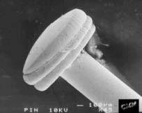


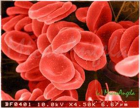

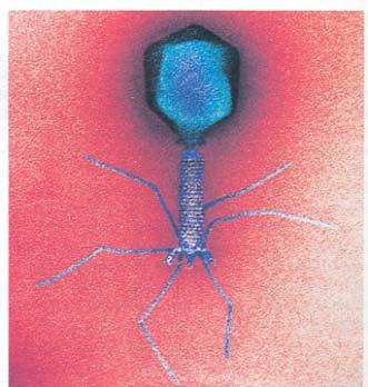
4 Things Natural 10-2 m How small is nano? Things Manmade Ant ~ 5 mm 10-3 m Head of a pin 1-2 mm Human hair ~50 micron wide Micro world 10-4 m 10-5 m MicroElectroMechanical Systems (MEMS) micron wide 10-6 m Virus, ~100nm Red blood cells ~ 2-5 micron Nano world (1-100nm) 10-7 m 10-8 m 10-9 m Intel transistor Nanorobot Au nanoparticles 13 nm & 50 nm DNA ~2 nm diameter m Carbon nanotube ~2 nm diameter Adapted from office of Basic Energy Sciences Office of Science
5 Why go to nano? L: length Integrated circuit: faster, more function, lower power consumption Data storage: higher capacity ( 1/L 2 ), 1Tbits/in 2 25nm 25nm/bit Semiconductor: quantum confined phenomena (quantum dots/wells ) Magnetism: single domain formation at L<magnetic domain wall thickness, superparamagnetism Photonics: new phenomena at L<λ photonic crystal, negative refractive index, near field optics, plasmonics Biomedical: DNA sorting (nanofluidics), drug delivery (nanoparticles) Chemistry: higher surface area higher reactivity for catalyst, higher sensitivity for chemical sensors
6 How to reach nano? Bottom up (chemical): assemble small building blocks (atoms ) into larger structures chemical synthesis, self assembly nanoparticle, nanowire, nanotube low cost, high resolution (~few nm), 3D (sphere) Top down (engineering): modify large object to give smaller features lithography, thin film deposition, etching expensive, precise control of size/shape and positioning Top down approach: three components Lithography: generate pattern in a material called resist photolithography, electron-beam lithography, nanoimprint lithography Thin film deposition (growth): spin coating, chemical vapor deposition, molecular beam epitaxy, sputtering, evaporation, electroplating Etching (removal): reactive ion etching, ion beam etching, wet chemical etching, polishing Semiconductor industry uses top down approach
7 Lithographies: a comparison Photolithography: duplicate pattern on the photo-mask into photo-resist fast, low resolution (~λ), standard for micro-fabrication Electron beam lithography: generate pattern by serial writing into a resist slow (1 wafer/day), high resolution (~10nm) Nanoimprint lithography: duplicate mold pattern into a polymer resist fast, high resolution (2nm), low cost NIL is the choice for nanoscale patterning over large surface area
 force UV-curable NIL")
. Softened and patterned at high T.")


8 Nanoimprint lithography (NIL) Thermal NIL (hot embossing lithography) force UV-curable NIL UV-illumination mold Rigid resist at room temperature (RT). Softened and patterned at high T. De-emboss at low temperature. Simple and low cost resist polymers, for general applications. Soft liquid resist, patterned at RT Hardened by UV-induced polymerization No thermal cycle, targeted for semiconductor industry requiring accurate alignment
9 Nanofabrication: one example metal nanostructures side view Metal nanostructures substrate substrate resist (polymer) Direct etch process resist (polymer) Liftoff process 1. Thin film growth 1. Thin film growth 2. Lithography 2. Lithography 3. Etching 3. Deposition 4. Etching (dissolve resist) 4. Etching (dissolve resist) 3-5 steps to pattern each layer, computer chip has >15 layers


 70 nm diameter")
10 One more step: 200nm period pillar array with various diameters 35 nm diameter Cr silicon 1. Cr dots by liftoff 2. RIE silicon and remove Cr (RIE: reactive ion etching) 70 nm diameter 115 nm diameter
 Fluorescence Intensity 160 140 120 100 80 60 Bare control surface (no pillars) Bare SiO 2 control surface (no posts) 30 nm;")

11 Application: cell-antibody interaction For a fixed pitch of 200nm # of antibody a cell interacts pillar surface area (diameter) antibodies/cell T4 cell antibody SiO 2 pillar Y Y Y Y Y Y Y Y Averaged Fluorescence Intensity (arbitrary units) Fluorescence Intensity Bare control surface (no pillars) Bare SiO 2 control surface (no posts) 30 nm; 287 antibodies/cell 3185 antibodies/cell 100 nm; ~3185 antibodies/cell Goal: study how many antibody molecules are required to activate a cell. Activation represented by the upward slope of the fluorescence curve. Collaboration with MIT/Northeastern University (ongoing) Time (min) (min) More antibodies, shorter cell activation time
12 Summary for Part I 1. Nano-science studies the length range 1nm-100nm 2. New physics and applications appear at nanoscale, or just better performance 3. Two approaches for arriving at nano: bottom up and top down 4. Three components for top down approach: lithography, thin film deposition and etching. 5. Nanoimprint lithography is a molding process having high throughput and high resolution.
13 Outline Part I: Introduction What is nano? Why nano? How to reach nano? Micro and nano-fabrication: lithography, etching, thin film deposition One example of nanofabrication Part II: Nanoimprint lithography (NIL) (hot embossing) Hot embossing of several materials Polystyrene (biocompatible) Poly(lactic-co-glycolic acid) (biodegradable) MEH-PPV (semiconducting polymer for plastic solar cell) Metal (pulsed laser melting) Replication of 100nm to mm-scale features by thermal NIL Part III: Plasmonic chemical/biosensors based on metallic nanostructures Introduction to plasmon DNA hybridization detection by surface plasmon resonance (SPR) Surface enhanced Raman scattering (SERS) Raman scattering and SERS fundamentals Fabrication of nano-prism array as SERS active substrates SERS detection of R6G molecules and peptides Fabrication of nano-pyramid, nano-ring/crescent and nano-star (brief)

14 Hot embossing of polystyrene (biocompatible) 4µm period grating grating substrate Application: contact guidance of cell growth Definition: anisotropic topographic features induce cells to align along the direction of the anisotropy. Importance: in tissue engineering, if tissue is to be repaired, the new cells must be aligned and positioned correctly. cell Collaboration with LOEX of Laval University
.")
15 Corneal and dermal cell growth Corneal cell Dermal cell Day 1 grating first layer Day 12 first layer second layer First layer: both cells aligned with the grating (as expected). Second layer: Corneal cells - oriented at 60 relative to first layer, as in a native cornea Dermal cells - no orientation Guillemette, Cui Nature Methods, to be submitted
 Application: Brain repair: grow neuron cells on PLGA gratings and transplant it into brain. The support PLGA will disappear in 1-2 months (as it is biodegradable).")
16 Hot embossing of PLGA (poly(lactic-co-glycolic acid)) (biodegradable, biocompatible) 2µm 30µm 25µm 70µm PLGA Aspect ratio: >10:1 SEM image of 30µm period PLGA grating (SEM: scanning electron microscopy) Application: Brain repair: grow neuron cells on PLGA gratings and transplant it into brain. The support PLGA will disappear in 1-2 months (as it is biodegradable). Collaboration with NRC-Institute for Biological Sciences

17 Hot embossing of semiconducting polymers SEM image of 200nm period MEH-PPV grating MEH-PPV 1 µm CH 3 O CH CH n MEH-PPV Tg=65 o C. Hot embossing at 120 o C and 20bar. MEH-PPV spun on a PEDOT/ITO/glass. Collaboration with Organic Vision Inc. and McGill University
/Alq3(n)/Al Plastic solar cells: flexible, light weight, tunable electrical properties, and potential lower fabrication")
18 Application: nanostructured plastic solar cell Glass ITO P N Al Classic planar p-n junction, low junction area, low efficiency Metal electrode N P ITO Transparent substrate Nanostructured junction, high junction area, high efficiency 200nm Layers: glass/ito/pedot/meh- PPV(p)/Alq3(n)/Al Plastic solar cells: flexible, light weight, tunable electrical properties, and potential lower fabrication cost. Limitation: low energy conversion efficiency due to low carrier mobility. Method to increase efficiency: increase the interface area by nanopatterning the p-n junction. Cui, NNT, 2004

 Here Ni and Cu were patterned and the step took only")
19 Hot embossing of metal using pulsed laser metal laser pulse 200nm period nickel grating Copper grating mold substrate - XeCl pulsed excimer laser, λ=308nm, τ=20ns, J/cm 2. - Lines rounded due to surface tension and volume shrinking upon solidification Metals are generally more difficult to pattern due to lack of suitable RIE process (RIE: reactive ion etching) Here Ni and Cu were patterned and the step took only ~100ns with minimal heating of the substrate Cui, manuscript in preparation
20 Outline Part I: Introduction What is nano? Why nano? How to reach nano? Micro and nano-fabrication: lithography, etching, thin film deposition One example of nanofabrication Part II: Nanoimprint lithography (NIL) (hot embossing) Hot embossing of several materials Polystyrene (biocompatible) Poly(lactic-co-glycolic acid) (biodegradable) MEH-PPV (semiconducting polymer for plastic solar cell) Metal (pulsed laser melting) Replication of 100nm to mm-scale features by thermal NIL Part III: Plasmonic chemical/biosensors based on metallic nanostructures Introduction to plasmon DNA hybridization detection by surface plasmon resonance (SPR) Surface enhanced Raman scattering (SERS) Raman scattering and SERS fundamentals Fabrication of nano-prism array as SERS active substrates SERS detection of R6G molecules and peptides Fabrication of nano-pyramid, nano-ring/crescent and nano-star (brief)
 Chou, J. Vac. Sci. Technol. B, 1997 P = γ 2πR πr 2γ R = 2 1 R Pressure 1/diameter.")

21 NIL for small features (<10nm) Press liquid into a nano-hole Pressure (P) F=γ 2πR Surface tension (γ) Thermal NIL into PMMA (10nm pillar array mold) Chou, J. Vac. Sci. Technol. B, 1997 P = γ 2πR πr 2γ R = 2 1 R Pressure 1/diameter. But for protruded mold features (pillars ), local pressure at the pillar is much higher than average - easy to imprint. UV-curable NIL, 2nm carbon nanotube mold Hua, Nano Lett NIL not difficult for nano, especially for protruded mold features
22 NIL for large features (>100 µm) - simultaneous pattern duplication of large and small features Application: large features needed to connect small ones to the outside world (electrodes ). Challenge: more polymer must be displaced over longer distances. A popular approach: two-step process - small features by NIL, large ones by photolithography. Previously, pattern size of 100µm duplicated by thermal NIL. Here, we will demonstrate pattern duplication of nm mm features. More challenging to duplicate large features than small ones
23 Modeling of liquid flow for large features (>>pattern depth) L L L mold h 0 h 0 Liquid Substrate Assumptions: periodic mold structure (period 2L) ignore inertial, gravitational forces and surface tension resist film thickness = mold trench depth = h 0 L = 2h 0 3 pτ p µ τ µ 1/ 2 L: achievable feature size p: pressure τ: imprinting time µ: viscosity h 0 : film thickness Achievable feature size depends on pressure, time and viscosity of molten polymer
24 Strategy to imprint large features (mm) 1/ 2 τ 1 L p µ µ L: achievable feature size p: pressure τ: melting time µ: viscosity For PMMA at T>Tg=105 o C (glass transition temperature) log µ = nlog M 12.21( T T g w ( T T g ) ) const M w : molecular weight n=1 for M w <M C, un-entangled molecules n=3.4 for M w >M C, entangled molecules Viscosity for PMMA (M c =30kg/mol) a) 12 kg/mol, 200 o C b) 12 kg/mol,150 o C c) 120 kg/mol, 200 o C µ a :µ b :µ c =1:126:278 Use low molecular weight PMMA and imprint at high temperature

25 Square (mm) imprinted into PMMA Optical image Profile Strategy to imprint large features (mm) But for nanoscale features 200nm 2mm after excessive etch Schematic mold wafer Such a profile makes liftoff difficult. Solution: use tri-layer resist system resist need to etch silicon wafer Need excessive etch to remove the thick resist at the square center tri-layer resist PMMA bottom polymer layer thin SiO 2 Need excessive resist etch and tri-layer resist for large features
26 Fabrication process flow Mold tri-layer resist PMMA: Polymethyl methacrylate. ARC: Anti-reflection coating, crosslinked polymer. RIE: Reactive ion etching 1. Imprint PMMA SiO 2 ARC silicon wafer 2. RIE PMMA (excessive etch) 4. RIE ARC (O 2 gas, etch little SiO 2 ) Cr 5. Evaporate Cr 6. Liftoff Cr (dissolve ARC) 3. RIE SiO 2 (CHF 3 gas) 7. RIE Si (etch little Cr) Fabrication is liftoff process using tri-layer resist plus etching
 Line-width in the mold is 80nm Line-width in the duplicated pattern is 98nm 50 40 30 98nm")
. For large features, 1.")
27 Result of pattern duplication of nano-grating and mm-square 1.3mm square Line-width change (nm) Line-width in the mold is 80nm Line-width in the duplicated pattern is 98nm nm Duplicated square size (µm) L 1 µ PMMA etched (nm) Viscosity (µ/ µ o ) -1/2 For small features, line-width increased by ~18nm (acceptable). For large features, 1.3mm squares faithfully duplicated (one order higher than previously achieved). Cui, Microelectronic Engineering, 2006
28 Summary for Part II 1. Hot embossing can pattern various functional polymer materials: biocompatible, biodegradable, semiconducting 2. It is not so difficult for NIL to achieve high resolution (<5nm) 3. It is more challenging to pattern large features (>100µm) 4. We have demonstrated simultaneous pattern duplication of nm to mm-scale feature
29 Outline Part I: Introduction What is nano? Why nano? How to reach nano? Micro and nano-fabrication: lithography, etching, thin film deposition One example of nanofabrication Part II: Nanoimprint lithography (NIL) (hot embossing) Hot embossing of several materials Polystyrene (biocompatible) Poly(lactic-co-glycolic acid) (biodegradable) MEH-PPV (semiconducting polymer for plastic solar cell) Metal (pulsed laser melting) Replication of 100nm to mm-scale features by thermal NIL Part III: Plasmonic chemical/biosensors based on metallic nanostructures Introduction to plasmon DNA hybridization detection by surface plasmon resonance (SPR) Surface enhanced Raman scattering (SERS) Raman scattering and SERS fundamentals Fabrication of nano-prism array as SERS active substrates SERS detection of R6G molecules and peptides Fabrication of nano-pyramid, nano-ring/crescent and nano-star (brief)

 surface t=0 -σ 0 +σ 0 E ext t=t/2=π/ω (half period) E ext Localized surface plasmon: plasmon")
30 Annu. Rev. Phys. Chem 2007 Plasmon: collective oscillation of free electrons (has nothing to do with plasma TV (ionized gas)) Plasmon: bulk, surface, localized E ext = E 0 e iω t iω t σ = σ e 0 Surface plasmon: plasmon confined to (metal) surface t=0 -σ 0 +σ 0 E ext t=t/2=π/ω (half period) E ext Localized surface plasmon: plasmon confined to (metal) nano-structures Metal nano-sphere 2 2 4πne ω p = ~ frequency of m visible light

 ω(plasmon) The British Museum. http://www.thebritishmuseum.ac.")
31 Lycurgus Cup of the 4 th Century Green = Reflected Light Red = Transmitted Light Image of Ag/Au nanoparticle in the Lycurgus cup Color is due to resonant absorption of light, which excites localized surface plasmon when ω(light) ω(plasmon) The British Museum. (March 2004)
 Reflected light Angle of incidence - Excitation of surface plasmon by")
32 Surface plasmon resonance (SPR) biosensor SPR: excitation of surface plasmon by light Plasmon frequency is very sensitive to changes on metal surface Application: biosensor (DNA, protein ) target bio-molecule ω = target molecule ω ω + ω p ω o absorption of p = o glass θ prism Gold 50nm Reflectivity Light in (λ=800nm) Reflected light Angle of incidence - Excitation of surface plasmon by evanescent wave - Resonant absorption occurs at certain angle θ SPR sensor detects change in thickness/refractive index on metal surface
 and propagating (from underlying continuous film) surface plasmon. 2. Increasing the surface area for DNA binding.")
33 Enhanced DNA hybridization detection by SPR on periodic Au nano-post array Au nano-post Au nano-posts increase sensitivity by: 1. Coupling between localized (from nano-posts) and propagating (from underlying continuous film) surface plasmon. 2. Increasing the surface area for DNA binding. Au film ssdna (ss: single strand) dsdna (ds: double strand) Au DNA hybridization leads to a change in - - refractive index by 5% - thickness by 3.5nm Collaboration with McGill University
 35 nm 50 nm 75 nm 90 nm film (no post) 250nM DNA target buffer SEM image of Au nano-post array on 20nm flat Au film 0.")
34 Enhanced SPR detection of DNA hybridization Reflectivity (%) Post diameter (fixed period 110nm, height 30nm ) 35 nm 50 nm 75 nm 90 nm film (no post) 250nM DNA target buffer SEM image of Au nano-post array on 20nm flat Au film Time (min) ssdna hybridization dsdna Sensitivity was enhanced by 5 when post diameter = 50nm Malic, Cui Optics Letters, 2007
35 Outline Part I: Introduction What is nano? Why nano? How to reach nano? Micro and nano-fabrication: lithography, etching, thin film deposition One example of nanofabrication Part II: Nanoimprint lithography (NIL) (hot embossing) Hot embossing of several materials Polystyrene (biocompatible) Poly(lactic-co-glycolic acid) (biodegradable) MEH-PPV (semiconducting polymer for plastic solar cell) Metal (pulsed laser melting) Replication of 100nm to mm-scale features by thermal NIL Part III: Plasmonic chemical/biosensors based on metallic nanostructures Introduction to plasmon DNA hybridization detection by surface plasmon resonance (SPR) Surface enhanced Raman scattering (SERS) Raman scattering and SERS fundamentals Fabrication of nano-prism array as SERS active substrates SERS detection of R6G molecules and peptides Fabrication of nano-pyramid, nano-ring/crescent and nano-star (brief)
36 SERS (surface enhanced Raman spectroscopy) fundamentals Molecular vibration: Molecular vibrational energy quantized (phonon). Its frequency lies in infrared (IR) spectral range. IR spectroscopy is used to identity a material. (strong absorption when ν(photon)=ν(phonon)) incident light atom scattered light ν ( photon) = ν 0 ± ν ( phonon) Raman scattering: Inelastic light scattering from a sample with a shift in frequency by the energy of its characteristic molecular vibrations (phonon). It detects symmetric vibration, which complements IR spectroscopy. The vibration information is transferred from IR to visible, where brighter sources and more efficient detectors are available. SERS effect: enormous enhancement (up to ) of Raman scattering when a molecule is adsorbed on nanostructured metallic surface. This arises from two main mechanisms - Electromagnetic effect (dominant): localized surface plasmon resonance. (Raman intensity E 4 ) Chemical effect: electronic coupling between molecule and metal. metal nanostructure E>>E ext
37 SERS advantages, approaches to generate SERS-active surfaces Advantage of SERS: (3 S ) Sensitivity - high, single molecule detection demonstrated Selectivity - high, fingerprint of each type of molecule Speed - high, few seconds High field at tiny gaps High field at sharp corners, or tiny gaps if close enough Metallic particles (chemical synthesis) Metal nanostructure Nanofabricated metal structures - tunable resonant wavelength, homogeneous size/shape, more reproducible and reliable SERS detection

.")
38 One example: nanoprism (triangular nanostructure) Motivation: Localized surface plasmon resonance can be tuned systematically by varying the size, shape and height of the nanoprism. Sharp corners of the nanoprism lead to a strong local electromagnetic field enhancement. Horizontal polarization Low electrical field Vertical polarization nanoprism High field spots Previous fabrication method: Chemical approach: reduction of metal salts (difficult). Light-induced aggregation of small nanoparticle seeds (low yield and none-homogeneous) Nanoprism: tune plasmon resonance, enhance local electrical field Jin, Science, 294, 1901(2001)
39 Direction of angle evaporation of Ti Fabrication principle PMMA pyramid by NIL with a mold having inverse-pyramid-shaped hole PMMA pyramid PMMA: Polymethyl methacrylate NIL: Nanoimprint lithography RIE: Reactive ion etching Si wafer 1. NIL into PMMA Ti 3. RIE PMMA Cr/Ag prism 2. Evaporate Ti at large angle Again, it is a liftoff process 4. Evaporate and liftoff metal
 crystalline plane, forming an inverse-pyramidshaped hole.")
40 Fabrication of mold with inversepyramid-shaped hole array (111) SiO 2 mask Si (100) KOH etch Si (111) direction 100 times slower than other crystalline planes. So etching will stop at (111) crystalline plane, forming an inverse-pyramidshaped hole. SEM image of the mold (SEM: scanning electron microscopy) KOH etching of crystalline Si is anisotropic
/Ag(20nm) Raman Shift (cm -1 ) Raman measurement: excitation laser λ=785nm, power 0.16mW/mm 2, beam spot size 25-30µm, collection time 3sec.")
41 SERS detection of rhodamine 6G (R6G) molecule SEM image of 200nm period nanoprism Raman Intensity (arb. units) Si nanoprism array of Cr(2.5nm)/Ag(20nm) Raman Shift (cm -1 ) Raman measurement: excitation laser λ=785nm, power 0.16mW/mm 2, beam spot size 25-30µm, collection time 3sec. Raman signal from ~monolayer R6G is nearly comparable to that from bulk silicon Cui, Nanotechnology, 2008

42 Effect of Cr (adhesion layer) on SERS Ag Cr Raman Intensity (counts) Cr(1)/Au(30) Cr(5)/Au(30) 1180 Ag(20nm) Raman Shift (cm -1 ) Why Cr is detrimental to SERS? Electric permittivity ε= ε 1 +i ε 2 Strong SERS requires large ε 1 (strong charge oscillation) and small ε 2 (low loss) But at λ=800 nm ε 1 (Cr)/ε 1 (Ag)=1/20 ε 2 (Cr)/ε 2 (Ag)=50/1 Keep Cr adhesion layer as thin as possible (1nm) Cr(5nm)/Ag(20nm)
43 Numerical calculation by discrete dipole approximation (to optimize nanoprism dimension) Absorption efficiency Ag(20nm) Ag+Cr(5nm) Ag+Cr+SiO 2 Ag+SiO 2 2x2 Array Ag(60nm) Laser λ=785nm Cr (promote adhesion) Ag SiO 2 silicon For single Ag nanoprism, λ res ~720nm. Cr decreases absorption efficiency. SiO 2 substrate red-shift λ res by 100nm. Thicker Ag decreases λ res λ (nm) 2 2 array has higher λ res Discrete Dipole Approximation (DDA): It computes scattering of light by wavelength-scale structures. The structure is represented by an array of dipoles located in a regular cubic lattice. Advantage: only the domain of interest (the metal nanostructure) is discretized.
 abuse in sports (doping).")
44 SERS detection of biomolecules Challenges: Bio-molecules compose of similar repeating units (base for DNA, amino acid for protein), hence their Raman spectra are very similar Solution: Attach a tag molecule to the biomolecule, but no longer label-free Collect large number of spectra and do regression date analysis Application: Detection of drug (e.g. recombinant proteins) abuse in sports (doping). H: Human; B: Bovine; S: Sheep; CRF: Corticotropin releasing factors Collaboration with NRC National Institute for Nanotechnology Raman Shift (cm -1 )
. D. Contour plot for the three CRFs and their 12 mixtures (B+C).")
45 Regression Data Analysis Collected 798 spectra per sample Partial least-squares regression A. Score plot representing the first two principal components. B. Contour plot showing the correlation for the three CRFs. C. Contour plot for their mixtures ( contaminated samples). D. Contour plot for the three CRFs and their 12 mixtures (B+C). SERS can distinguish bio-molecules, but need collect large number of spectra Alvarez-Puebla, Cui ChemMedChem, 2007
46 Outline Part I: Introduction What is nano? Why nano? How to reach nano? Micro and nano-fabrication: lithography, etching, thin film deposition One example of nanofabrication Part II: Nanoimprint lithography (NIL) (hot embossing) Hot embossing of several materials Polystyrene (biocompatible) Poly(lactic-co-glycolic acid) (biodegradable) MEH-PPV (semiconducting polymer for plastic solar cell) Metal (pulsed laser melting) Replication of 100nm to mm-scale features by thermal NIL Part III: Plasmonic chemical/biosensors based on metallic nanostructures Introduction to plasmon DNA hybridization detection by surface plasmon resonance (SPR) Surface enhanced Raman scattering (SERS) Raman scattering and SERS fundamentals Fabrication of nano-prism array as SERS active substrates SERS detection of R6G molecules and peptides Fabrication of nano-pyramid, nano-ring/crescent and nano-star (brief)

47 Other types of nanostructures fabricated by NIL: nano-pyramid Fabrication principle: 1. Triangular hole array 2. Deposit thin film 3. Deposit thick film 3. Liftoff Opening close-up gradually due to lateral deposition Nano-prism (2D) Nano-pyramid (3D)
 200nm 1.")

 Near field for nano-crescent 3.")
48 Nano-ring and nano-crescent Fabrication principle: Nanoring (red) defined by edge of nanodisk (blue) 200nm 1. Hole array with large undercut Cr deposition at an angle Cr nano-disk Nano-ring Nano-crescent 2. Deposit Cr to cover hole bottom Reactive gas High field spots c) d) Near field for nano-crescent 3. RIE with lateral etch Cui, Microelectronic Engineering 2007; Li, Cui Nanotechnology 2008
 200nm 2.")
 formed when adjacent holes")
49 Fabrication principle: Nano-star array 1. Nano-hole array (blue color) 200nm 2. Enlarge holes due to lateral etching High field spots 3. Nano-stars (red color) formed when adjacent holes touch each other Cui SPIE 2008
50 Summary for Part III 1. Plasmon is collective oscillation of free electrons 2. Three types of plasmon: bulk, surface and localized 3. Surface plasmon resonance can be used for biosensors 4. We achieved 5 higher SPR sensitivity by patterning Au nano-post array on a flat Au film 5. SERS is an enormous enhancement of Raman scattering when a molecule is adsorbed on a nanostructured metallic surface 6. Using nanoimprint lithography, we fabricated arrays of nano-prism, nano-pyramid, nano-ring/crescent and nano-star. 7. We demonstrated SERS detection of R6G molecules, as well as peptides classification.
51 Acknowledgement CNRC-IMI: Teodor Veres (group leader) Collaborators: -LOEX (Laval University): M. Guillemette, FA Auger, L. Germain -McGill University: L. Malic, M. Tabrizian -MIT/Northeastern University: X. Cheng, S. Murthy, M. Toner -NINT: R. Alvarez-Puebla, H. Fenniri -Organic Vision Inc.: S. Xiao
52
Plasmonics using Metal Nanoparticles. Tammy K. Lee and Parama Pal ECE 580 Nano-Electro-Opto-Bio
 Plasmonics using Metal Nanoparticles Tammy K. Lee and Parama Pal ECE 580 Nano-Electro-Opto-Bio April 1, 2007 Motivation Why study plasmonics? Miniaturization of optics and photonics to subwavelength scales
In-Situ Monitoring of Pattern Filling in Nano-Imprint Lithography Using Surface Plasmon Resonance
 Copyright 2011 American Scientific Publishers All rights reserved Printed in the United States of America Journal of Nanoscience and Nanotechnology Vol. 11, 1 6, 2011 In-Situ Monitoring of Pattern Filling
Nanoimprinting in Polymers and Applications in Cell Studies. Albert F. YEE Chemical Engineering & Materials Science UC Irvine
 Nanoimprinting in Polymers and Applications in Cell Studies Albert F. YEE Chemical Engineering & Materials Science UC Irvine Presentation outline Motivation Reversal imprinting Soft inkpad imprinting on
Introduction to Lithography
 Introduction to Lithography G. D. Hutcheson, et al., Scientific American, 290, 76 (2004). Moore s Law Intel Co-Founder Gordon E. Moore Cramming More Components Onto Integrated Circuits Author: Gordon E.
Title: Localized surface plasmon resonance of metal nanodot and nanowire arrays studied by far-field and near-field optical microscopy
 Contract Number: AOARD-06-4074 Principal Investigator: Heh-Nan Lin Address: Department of Materials Science and Engineering, National Tsing Hua University, 101, Sec. 2, Kuang Fu Rd., Hsinchu 30013, Taiwan
Chapter 7 NANOIMPRINTED CIRCULAR GRATING DISTRIBUTED FEEDBACK DYE LASER
 Chapter 7 66 NANOIMPRINTED CIRCULAR GRATING DISTRIBUTED FEEDBACK DYE LASER 7.1 Introduction In recent years, polymer dye lasers have attracted much attention due to their low-cost processing, wide choice
Vertically aligned Ni magnetic nanowires fabricated by diblock-copolymer-directed Al thin film anodization
 Vertically aligned Ni magnetic nanowires fabricated by diblock-copolymer-directed Al thin film anodization Researcher: Kunbae (Kevin) Noh, Graduate Student, MAE Dept. and CMRR Collaborators: Leon Chen,
CREOL, The College of Optics & Photonics, University of Central Florida
 Metal Substrate Induced Control of Ag Nanoparticle Plasmon Resonances for Tunable SERS Substrates Pieter G. Kik 1, Amitabh Ghoshal 1, Manuel Marquez 2 and Min Hu 1 1 CREOL, The College of Optics and Photonics,
General Introduction to Microstructure Technology p. 1 What is Microstructure Technology? p. 1 From Microstructure Technology to Microsystems
 General Introduction to Microstructure Technology p. 1 What is Microstructure Technology? p. 1 From Microstructure Technology to Microsystems Technology p. 9 The Parallels to Microelectronics p. 15 The
Introduction to Nanoscience and Nanotechnology
 Introduction to Nanoscience and Nanotechnology ENS 463 2. Principles of Nano-Lithography by Alexander M. Zaitsev alexander.zaitsev@csi.cuny.edu Tel: 718 982 2812 Office 4N101b 1 Lithographic patterning
Applications of Nano Patterning Process 1. Patterned Media
 Applications of Nano Patterning Process 1. Patterned Media Contents Introduction Part. 1. Nanoimprinting on Glass Substrate for Patterned Media Part. 2. Nanoinjection Molding of Nanopillars for Patterned
Compact hybrid plasmonic-si waveguide structures utilizing Albanova E-beam lithography system
 Compact hybrid plasmonic-si waveguide structures utilizing Albanova E-beam lithography system Introduction Xu Sun Laboratory of Photonics and Microwave Engineering, Royal Institute of Technology (KTH),
Introduction to Micro/Nano Fabrication Techniques. Date: 2015/05/22 Dr. Yi-Chung Tung. Fabrication of Nanomaterials
 Introduction to Micro/Nano Fabrication Techniques Date: 2015/05/22 Dr. Yi-Chung Tung Fabrication of Nanomaterials Top-Down Approach Begin with bulk materials that are reduced into nanoscale materials Ex:
NanoFabrication Systems DPN. Nanofabrication Systems. A complete line of instruments and tools for micro and nanopatterning applications
 DPN Nanofabrication Systems A complete line of instruments and tools for micro and nanopatterning applications DPN Nanofabrication Systems A complete line of instruments and tools for micro and nanopatterning
Lecture 22: Integrated circuit fabrication
 Lecture 22: Integrated circuit fabrication Contents 1 Introduction 1 2 Layering 4 3 Patterning 7 4 Doping 8 4.1 Thermal diffusion......................... 10 4.2 Ion implantation.........................
Chapter 3 Silicon Device Fabrication Technology
 Chapter 3 Silicon Device Fabrication Technology Over 10 15 transistors (or 100,000 for every person in the world) are manufactured every year. VLSI (Very Large Scale Integration) ULSI (Ultra Large Scale
Superionic Solid State Stamping (S4)
") Superionic Solid State Stamping (S4) Lead Faculty Researcher: Placid Ferreira Department: Materials Science & Engineering Hsu et al, Nano Letters, 2007 1. Description: This dry, single step, electrochemical
Superionic Solid State Stamping (S4) Lead Faculty Researcher: Placid Ferreira Department: Materials Science & Engineering Hsu et al, Nano Letters, 2007 1. Description: This dry, single step, electrochemical
UV15: For Fabrication of Polymer Optical Waveguides
 CASE STUDY UV15: For Fabrication of Polymer Optical Waveguides Master Bond Inc. 154 Hobart Street, Hackensack, NJ 07601 USA Phone +1.201.343.8983 Fax +1.201.343.2132 main@masterbond.com CASE STUDY UV15:
Tunable Nanoscale Plasmon Antenna for Localization and Enhancement of Optical Energy. Douglas Howe
 Tunable Nanoscale Plasmon Antenna for Localization and Enhancement of Optical Energy Douglas Howe Applied Optics Spring 2008 Table of Contents Abstract... 3 Introduction... 4 Surface Plasmons... 4 Nano
Nanofabrication Prof. Stephen Y. Chou NanoStructure Laboratory
 Nanofabrication Prof. Stephen Y. Chou Department of Electrical Engineering Princeton University 1 Acknowledgment Dr. Paul Fischer Dr. Yun Wang Dr. Jay Guo Dr. Peter Klauss Dr. Jim Wang Dr. Longtin He Dr.
Surface Plasmon Resonance Analyzer
 Surface Plasmon Resonance Analyzer 5 6 SPR System Based on Microfluidics Wide Dynamic Range Kinetic Analysis by Detection of Association /Dissociation of Bio-Molecules Measuring of Mass Change below
A discussion of crystal growth, lithography, etching, doping, and device structures is presented in
 Chapter 5 PROCESSING OF DEVICES A discussion of crystal growth, lithography, etching, doping, and device structures is presented in the following overview gures. SEMICONDUCTOR DEVICE PROCESSING: AN OVERVIEW
Mater. Res. Soc. Symp. Proc. Vol Materials Research Society
 Mater. Res. Soc. Symp. Proc. Vol. 940 2006 Materials Research Society 0940-P13-12 A Novel Fabrication Technique for Developing Metal Nanodroplet Arrays Christopher Edgar, Chad Johns, and M. Saif Islam
for Bioanalytical Applications
 Conferinţa Diaspora in Cercetarea Ştiinţifică şi Invăţămantul Superior din Romania Bucuresti, 21-24 Septembrie 2010 Multifunctional Plasmonic Nanosensors for Bioanalytical Applications Simion Astilean
Advanced Polymers And Resists For Nanoimprint Lithography
 Q U A L I T Y A S S U R A N C E MICROSYSTEMS & NANOSYSTEMS SPECIAL REPORT Advanced Polymers And Resists For Nanoimprint Lithography Numerous polymer systems specifically designed for nanoimprint lithography
Crystallographic Characterization of GaN Nanowires by Raman Spectral Image Mapping
 Crystallographic Characterization of GaN Nanowires by Raman Spectral Image Mapping Heerad Farkhoor, Adam Schwartzberg, Jeffrey Urban August 12, 2009 Abstract Obtaining structural information of nano-structured
Today s Class. Materials for MEMS
 Lecture 2: VLSI-based Fabrication for MEMS: Fundamentals Prasanna S. Gandhi Assistant Professor, Department of Mechanical Engineering, Indian Institute of Technology, Bombay, Recap: Last Class What is
Thermal Nanoimprinting Basics
 Thermal Nanoimprinting Basics Nanoimprinting is a way to replicate nanoscale features on one surface into another, like stamping copies are made by traditional fabrication techniques (optical/ebeam lith)
Micro-Nano Fabrication Research
 Micro-Nano Fabrication Research Technical Education Quality Improvement Programme 22-23 December 2014 Dr. Rakesh G. Mote Assistant Professor Department of Mechanical Engineering IIT Bombay rakesh.mote@iitb.ac.in;
ECE280: Nano-Plasmonics and Its Applications. Week5. Extraordinary Optical Transmission (EOT)
") ECE280: Nano-Plasmonics and Its Applications Week5 Extraordinary Optical Transmission (EOT) Introduction Sub-wavelength apertures in metal films provide light confinement beyond the fundamental diffraction
ECE280: Nano-Plasmonics and Its Applications Week5 Extraordinary Optical Transmission (EOT) Introduction Sub-wavelength apertures in metal films provide light confinement beyond the fundamental diffraction
EECS130 Integrated Circuit Devices
 EECS130 Integrated Circuit Devices Professor Ali Javey 9/13/2007 Fabrication Technology Lecture 1 Silicon Device Fabrication Technology Over 10 15 transistors (or 100,000 for every person in the world)
Fabrication and Layout
 ECEN454 Digital Integrated Circuit Design Fabrication and Layout ECEN 454 3.1 A Glimpse at MOS Device Polysilicon Aluminum ECEN 475 4.2 1 Material Classification Insulators Glass, diamond, silicon oxide
FABRICATION OF SWTICHES ON POLYMER-BASED BY HOT EMBOSSING. Chao-Heng Chien, Hui-Min Yu,
 Stresa, Italy, 26-28 April 2006 FABRICATION OF SWTICHES ON POLYMER-BASED BY HOT EMBOSSING, Mechanical Engineering Department, Tatung University 40 Chung Shan N. Rd. Sec. 3 Taipei, Taiwan ABSTRACT In MEMS
Low-cost, deterministic quasi-periodic photonic structures for light trapping in thin film silicon solar cells
 Low-cost, deterministic quasi-periodic photonic structures for light trapping in thin film silicon solar cells The MIT Faculty has made this article openly available. Please share how this access benefits
SCIENCE CHINA Technological Sciences. Replication of large area nanoimprint stamp with small critical dimension loss
 SCIENCE CHINA Technological Sciences RESEARCH PAPER March 2012 Vol.55 No.3: 600 605 doi: 10.1007/s11431-011-4695-3 Replication of large area nanoimprint stamp with small critical dimension loss MENG FanTao
Multiphoton lithography based 3D micro/nano printing Dr Qin Hu
 Multiphoton lithography based 3D micro/nano printing Dr Qin Hu EPSRC Centre for Innovative Manufacturing in Additive Manufacturing University of Nottingham Multiphoton lithography Also known as direct
Outline. Introduction to the LIGA Microfabrication Process. What is LIGA? The LIGA Process. Dr. Bruce K. Gale Fundamentals of Microfabrication
 Outline Introduction to the LIGA Microfabrication Process Dr. Bruce K. Gale Fundamentals of Microfabrication What is LIGA? The LIGA Process Lithography Techniques Electroforming Mold Fabrication Analyzing
Nanostructured Plasmonic Interferometers for Ultrasensitive Label-Free Biosensing. Fil Bartoli Lehigh University 4/9/2014
 Nanostructured Plasmonic Interferometers for Ultrasensitive Label-Free Biosensing Fil Bartoli Lehigh University 4/9/2014 P.C. Rossin College of Engineering and Applied Science Department of Electrical
Laser Micromachining of Bulk Substrates and Thin Films Celine Bansal
 Laser Micromachining of Bulk Substrates and Thin Films Celine Bansal Oxford Lasers Ltd Moorbrook Park Didcot, Oxfordshire, OX11 7HP Tel: +44 (0) 1235 810088 www.oxfordlasers.com Outline Oxford Lasers Importance
ELEC 3908, Physical Electronics, Lecture 4. Basic Integrated Circuit Processing
 ELEC 3908, Physical Electronics, Lecture 4 Basic Integrated Circuit Processing Lecture Outline Details of the physical structure of devices will be very important in developing models for electrical behavior
Nanotechnology Principles, Applications, Careers, and Education. Copyright 2011 The Pennsylvania State University
 Nanotechnology Principles, Applications, Careers, and Education Copyright 2011 The Pennsylvania State University Outline What are the principles of nanotechnology? What are some applications? What kind
CONTENTS. Introduction. NSOM Optical Fiber Probes
 CONTENTS Introduction NSOM Optical Fiber Probes AFM Probes AFM Probes Hard to achieve Force Constants and Resonance Frequencies Deep Trench AFM Probes Electrical and STM Probes Hollow AFM Nanopipette Probes
Soft Lithography. Jin-Goo Park. Materials and Chemical Engineering Hanyang University, Ansan. Electronic Materials and Processing Lab.
 Hanyang University Soft Lithography Jin-Goo Park Materials and Chemical Engineering Hanyang University, Ansan Electronic Materials and Processing Lab. Introduction to Soft Lithography Research Micro- Electro-
PHYS 534 (Fall 2008) Process Integration OUTLINE. Examples of PROCESS FLOW SEQUENCES. >Surface-Micromachined Beam
 Process Integration OUTLINE. Examples of PROCESS FLOW SEQUENCES. >Surface-Micromachined Beam") PHYS 534 (Fall 2008) Process Integration Srikar Vengallatore, McGill University 1 OUTLINE Examples of PROCESS FLOW SEQUENCES >Semiconductor diode >Surface-Micromachined Beam Critical Issues in Process
PHYS 534 (Fall 2008) Process Integration Srikar Vengallatore, McGill University 1 OUTLINE Examples of PROCESS FLOW SEQUENCES >Semiconductor diode >Surface-Micromachined Beam Critical Issues in Process
Innovative Roll-to-Roll Equipment & Material Development Suite
 Innovative Roll-to-Roll Equipment & Material Development Suite For Next Generation Technology from Carpe Diem Technologies and the University of Massachusetts Amherst By John Berg, Dimitur Benchev, James
Czochralski Crystal Growth
 Czochralski Crystal Growth Crystal Pulling Crystal Ingots Shaping and Polishing 300 mm wafer 1 2 Advantage of larger diameter wafers Wafer area larger Chip area larger 3 4 Large-Diameter Wafer Handling
Femtosecond micromachining in polymers
 Femtosecond micromachining in polymers Prof. Dr Cleber R. Mendonca Daniel S. Corrêa Prakriti Tayalia Dr. Tobias Voss Dr. Tommaso Baldacchini Prof. Dr. Eric Mazur fs-micromachining focus laser beam inside
Micromachining AMT 2505
 Micromachining AMT 2505 Shanmuga Raja.B (BVB0912004) Module leader : Mr. Raja Hussain Introduction Micromachining are inherently connected to the evolution of Micro Electro Mechanical Systems (MEMS). Decades
Choi, Jun-Hyuk Korea Institute of Machinery & Materials
 The 11 th US-Korea Nanosymposium Choi, Jun-Hyuk 2014. 09. 29 Korea Institute of Machinery & Materials About KIMM Nano-research Bldg Clean RM Five Research Divisions; 1. Advanced Manufacturing Sys. 2. Extreme
Directional Surface Plasmon Coupled Emission
 Journal of Fluorescence, Vol. 14, No. 1, January 2004 ( 2004) Fluorescence News Directional Surface Plasmon Coupled Emission KEY WORDS: Surface plasmon coupled emission; high sensitivity detection; reduced
Lecture 1A: Manufacturing& Layout
 Introduction to CMOS VLSI Design Lecture 1A: Manufacturing& Layout David Harris Harvey Mudd College Spring 2004 Steven Levitan Fall 2008 1 The Manufacturing Process For a great tour through the IC manufacturing
Dr. Priyabrat Dash Office: BM-406, Mob: Webpage: MB: 205
 Email: dashp@nitrkl.ac.in Office: BM-406, Mob: 8895121141 Webpage: http://homepage.usask.ca/~prd822/ MB: 205 Nonmanufacturing In continuation from last class... 2 Top-Down methods Mechanical-energy methods
Basics of Plasmonics
 Basics of Plasmonics Min Qiu Laboratory of Photonics and Microwave Engineering School of Information and Communication Technology Royal Institute of Technology (KTH) Electrum 229, 16440 Kista, Sweden http://www.nanophotonics.se/
High Sensitivity of Phase-based Surface Plasmon Resonance in Nano-cylinder Array
 PIERS ONLINE, VOL. 4, NO. 7, 2008 746 High Sensitivity of Phase-based Surface Plasmon Resonance in Nano-cylinder Array Bing-Hung Chen, Yih-Chau Wang, and Jia-Hung Lin Institute of Electronic Engineering,
WP7 JRA2 JRA2 Research on High Precision Manufacturing. Investigation of optimum NIL stamp fabrication method to copy sub-10 nm BCP features
 DELIVERABLE REPORT WP7 JRA2 JRA2 Research on High Precision Manufacturing D7.1 Investigation of optimum NIL stamp fabrication method to copy sub-10 nm BCP features M18 NFFA-Europe has received funding
LOW TEMPERATURE PHOTONIC SINTERING FOR PRINTED ELECTRONICS. Dr. Saad Ahmed XENON Corporation November 19, 2015
 LOW TEMPERATURE PHOTONIC SINTERING FOR PRINTED ELECTRONICS Dr. Saad Ahmed XENON Corporation November 19, 2015 Topics Introduction to Pulsed Light Photonic sintering for Printed Electronics R&D Tools for
Plasmonics: Application-oriented fabrication. Part 1. Introduction
 Plasmonics: Application-oriented fabrication Part 1. Introduction Victor Ovchinnikov Department of Aalto Nanofab Aalto University Espoo, Finland Alvar Aalto was a famous Finnish architect and designer
Supplementary Figure S1 Photograph of MoS 2 and WS 2 flakes exfoliated by different metal naphthalenide (metal = Na, K, Li), and dispersed in water.
, and dispersed in water.") Supplementary Figure S1 Photograph of MoS 2 and WS 2 flakes exfoliated by different metal naphthalenide (metal = Na, K, Li), and dispersed in water. Supplementary Figure S2 AFM measurement of typical LTMDs
Supplementary Figure S1 Photograph of MoS 2 and WS 2 flakes exfoliated by different metal naphthalenide (metal = Na, K, Li), and dispersed in water. Supplementary Figure S2 AFM measurement of typical LTMDs
EE40 Lec 22. IC Fabrication Technology. Prof. Nathan Cheung 11/19/2009
 Suggested Reading EE40 Lec 22 IC Fabrication Technology Prof. Nathan Cheung 11/19/2009 300mm Fab Tour http://www-03.ibm.com/technology/manufacturing/technology_tour_300mm_foundry.html Overview of IC Technology
Polymer-based optical interconnects using nano-imprint lithography
 Polymer-based optical interconnects using nano-imprint lithography Arjen Boersma,Sjoukje Wiegersma Bert Jan Offrein, Jeroen Duis, Jos Delis, Markus Ortsiefer, Geert van Steenberge, MikkoKarppinen, Alfons
Fabrication Technology, Part I
 EEL5225: Principles of MEMS Transducers (Fall 2003) Fabrication Technology, Part I Agenda: Oxidation, layer deposition (last lecture) Lithography Pattern Transfer (etching) Impurity Doping Reading: Senturia,
NanoSystemsEngineering: NanoNose Final Status, March 2011
 1 NanoSystemsEngineering: NanoNose Final Status, March 2011 The Nanonose project is based on four research projects (VCSELs, 3D nanolithography, coatings and system integration). Below, the major achievements
EUV optics lifetime Radiation damage, contamination, and oxidation
 EUV optics lifetime Radiation damage, contamination, and oxidation M. van Kampen ASML Research 10-11-2016 Preamble Slide 2 ASML builds lithography scanners High-resolution photocopiers Copies mask pattern
Lecture 5: Micromachining
 MEMS: Fabrication Lecture 5: Micromachining Prasanna S. Gandhi Assistant Professor, Department of Mechanical Engineering, Indian Institute of Technology, Bombay, Recap: Last Class E-beam lithography X-ray
Microfabrication of Integrated Circuits
 Microfabrication of Integrated Circuits OUTLINE History Basic Processes Implant; Oxidation; Photolithography; Masks Layout and Process Flow Device Cross Section Evolution Lecture 38, 12/05/05 Reading This
Enhanced Light Trapping in Periodic Aluminum Nanorod Arrays as Cavity Resonator
 Enhanced Light Trapping in Periodic Aluminum Nanorod Arrays as Cavity Resonator Rosure B. Abdulrahman, Arif S. Alagoz, Tansel Karabacak Department of Applied Science, University of Arkansas at Little Rock,
Photonics applications IV. Fabrication of GhG optical fiber Fabrication of ChG planar waveguide Fabrication of ChG PC structure
 Photonics applications IV Fabrication of GhG optical fiber Fabrication of ChG planar waveguide Fabrication of ChG PC structure 1 Why does fabrication issue matter for photonics applications? Geometrical
Absorption of an electromagnetic wave
 In vivo optical imaging?? Absorption of an electromagnetic wave Tissue absorption spectrum Extinction = Absorption + Scattering Absorption of an electromagnetic wave Scattering of an electromagnetic wave
Microelectronics. Integrated circuits. Introduction to the IC technology M.Rencz 11 September, Expected decrease in line width
 Microelectronics Introduction to the IC technology M.Rencz 11 September, 2002 9/16/02 1/37 Integrated circuits Development is controlled by the roadmaps. Self-fulfilling predictions for the tendencies
Efficient organic distributed feedback lasers with active films imprinted by thermal nanoimprint lithography
 Efficient organic distributed feedback lasers with active films imprinted by thermal nanoimprint lithography bidali zenuenean, ondo dago. Efficient organic distributed feedback lasers with active films
Silver Diffusion Bonding and Layer Transfer of Lithium Niobate to Silicon
 Chapter 5 Silver Diffusion Bonding and Layer Transfer of Lithium Niobate to Silicon 5.1 Introduction In this chapter, we discuss a method of metallic bonding between two deposited silver layers. A diffusion
Preface Preface to First Edition
 Contents Foreword Preface Preface to First Edition xiii xv xix CHAPTER 1 MEMS: A Technology from Lilliput 1 The Promise of Technology 1 What Are MEMS or MST? 2 What Is Micromachining? 3 Applications and
PATTERNING OF OXIDE THIN FILMS BY UV-LASER ABLATION
 Journal of Optoelectronics and Advanced Materials Vol. 7, No. 3, June 2005, p. 1191-1195 Invited lecture PATTERNING OF OXIDE THIN FILMS BY UV-LASER ABLATION J. Ihlemann * Laser-Laboratorium Göttingen e.v.,
Figure 2.3 (cont., p. 60) (e) Block diagram of Pentium 4 processor with 42 million transistors (2000). [Courtesy Intel Corporation.
 (e) Block diagram of Pentium 4 processor with 42 million transistors (2000). [Courtesy Intel Corporation.") Figure 2.1 (p. 58) Basic fabrication steps in the silicon planar process: (a) oxide formation, (b) selective oxide removal, (c) deposition of dopant atoms on wafer, (d) diffusion of dopant atoms into exposed
Figure 2.1 (p. 58) Basic fabrication steps in the silicon planar process: (a) oxide formation, (b) selective oxide removal, (c) deposition of dopant atoms on wafer, (d) diffusion of dopant atoms into exposed
Micro- and Nano-Technology... for Optics
 Micro- and Nano-Technology...... for Optics 3.2 Lithography U.D. Zeitner Fraunhofer Institut für Angewandte Optik und Feinmechanik Jena Electron Beam Column electron gun beam on/of control magnetic deflection
Chapter 4 Fabrication Process of Silicon Carrier and. Gold-Gold Thermocompression Bonding
 Chapter 4 Fabrication Process of Silicon Carrier and Gold-Gold Thermocompression Bonding 4.1 Introduction As mentioned in chapter 2, the MEMs carrier is designed to integrate the micro-machined inductor
Simple UV-based Soft-lithography Process for. Fabrication of Low-Loss Polymer PSQ-L-based. Waveguides
 Simple UV-based Soft-lithography Process for Fabrication of Low-Loss Polymer PSQ-L-based Waveguides Jie Teng 1, 2, 4, Stijn Scheerlinck 4, Geert Morthier 4, Roel Baets 4, Hongbo Zhang 2,3, Xigao Jian 2,3,
Complexity of IC Metallization. Early 21 st Century IC Technology
 EECS 42 Introduction to Digital Electronics Lecture # 25 Microfabrication Handout of This Lecture. Today: how are Integrated Circuits made? Silicon wafers Oxide formation by growth or deposition Other
PLASMONIC STRUCTURES IN PMMA RESIST
 PLASMONIC STRUCTURES IN PMMA RESIST Michal URBÁNEK a, Stanislav KRÁTKÝ a, MARCEL ŠIMÍK b, Vladimír KOLAŘÍK a, Miroslav HORÁČEK a, Milan MATĚJKA a a Institute of Scientific Instruments of the ASCR, v.v.i.,
Nanophotonics: principle and application. Khai Q. Le Lecture 11 Optical biosensors
 Nanophotonics: principle and application Khai Q. Le Lecture 11 Optical biosensors Outline Biosensors: Introduction Optical Biosensors Label-Free Biosensor: Ringresonator Theory Measurements: Bulk sensing
Photolithography I ( Part 2 )
") 1 Photolithography I ( Part 2 ) Chapter 13 : Semiconductor Manufacturing Technology by M. Quirk & J. Serda Bjørn-Ove Fimland, Department of Electronics and Telecommunication, Norwegian University of Science
1 Photolithography I ( Part 2 ) Chapter 13 : Semiconductor Manufacturing Technology by M. Quirk & J. Serda Bjørn-Ove Fimland, Department of Electronics and Telecommunication, Norwegian University of Science
Polymer-based Microfabrication
 Polymer-based Microfabrication PDMS SU-8 PMMA Hydrogel 1 Soft Lithography Developed by Whitesides, et. al A set of techniques for microfabrication based on the use of lithography, soft substrate materials
Roll-to-Roll Nanoimprint - 6 회 -
 Roll-to-Roll Nanoimprint - 6 회 - 목차 Click to add Title 1 Roll to Roll nanoimprint Introduction : Continuous Production System (Roll-to-Roll) Fabrication Processes Fabrication of nano roll mold 2 Case study
Fabrication of photonic band-gap crystals
 Fabrication of photonic band-gap crystals C. C. Cheng and A. Scherer California Institute of Technology, Pasadena, California 91125 Received 19 June 1995; accepted 9 August 1995 We describe the fabrication
Lecture 19 Microfabrication 4/1/03 Prof. Andy Neureuther
 EECS 40 Spring 2003 Lecture 19 Microfabrication 4/1/03 Prof. ndy Neureuther How are Integrated Circuits made? Silicon wafers Oxide formation by growth or deposition Other films Pattern transfer by lithography
Nano-imprinting Lithography Technology І
 Nano-imprinting Lithography Technology І Agenda Limitation of photolithograph - Remind of photolithography technology - What is diffraction - Diffraction limit Concept of nano-imprinting lithography Basic
Lecture 5. SOI Micromachining. SOI MUMPs. SOI Micromachining. Silicon-on-Insulator Microstructures. Agenda:
 EEL6935 Advanced MEMS (Spring 2005) Instructor: Dr. Huikai Xie SOI Micromachining Agenda: SOI Micromachining SOI MUMPs Multi-level structures Lecture 5 Silicon-on-Insulator Microstructures Single-crystal
REAGENTLESS SENSORS WAVEGUIDE GRATING COUPLING SENSORS MACH-ZEHNDER INTERFEROMETER SENSORS SURFACE PLASMON RESONANCE SENSORS
 REAGENTLESS SENSORS WAVEGUIDE GRATING COUPLING SENSORS MACH-ZEHNDER INTERFEROMETER SENSORS SURFACE PLASMON RESONANCE SENSORS Reagentless Grating Coupler Sensor Angle, θ, is related to the analyte refractive
M. Hasumi, J. Takenezawa, Y. Kanda, T. Nagao and T. Sameshima
 Proceedings of 6th Thin Film Materials & Devices Meeting November 2-3, 2009, Kyoto, Japan http://www.tfmd.jp/ Characterization of SiO x /Si Interface Properties by Photo Induced Carrier Microwave Absorption
Supplementary Figures
 Supplementary Figures Supplementary Figure 1. Mass spectrometry characterization of Au 25, Au 38, Au 144, Au 333, Au ~520 and Au ~940 nanoclusters. (a) MALDI-mass spectra of Au 144, Au 333, Au ~520 and
Supplementary Figure S1. Scheme for the fabrication of Au nanohole array pattern and
 Supplementary Figure S1. Scheme for the fabrication of Au nanohole array pattern and the growth of hematite nanorods on the Au nanohole array substrate. (a) Briefly, the 500 nm sized PS monolayer was assembled
Process steps for Field Emitter devices built on Silicon wafers And 3D Photovoltaics on Silicon wafers
 Process steps for Field Emitter devices built on Silicon wafers And 3D Photovoltaics on Silicon wafers David W. Stollberg, Ph.D., P.E. Research Engineer and Adjunct Faculty GTRI_B-1 Field Emitters GTRI_B-2
Chemical Vapor Deposition
 Chemical Vapor Deposition ESS4810 Lecture Fall 2010 Introduction Chemical vapor deposition (CVD) forms thin films on the surface of a substrate by thermal decomposition and/or reaction of gas compounds
Micro-fluidic Chip for Flow Cytometry Jeff Wang
 Micro-fluidic Chip for Flow Cytometry Jeff Wang September, 2015 ABSTRACT This lab course is intended to give students hands-on experience with microfabrication. The project is to make a micro-fluidic chip
Introduction to Nanofabrication: Top Down to Bottom Up
 Welcome to NACK s Webinar Introduction to Nanofabrication: Top Down to Bottom Up NACK is an NSF-funded ATE Resource Center supporting faculty in Nanotechnology Education Hosted by MATEC Networks www.matecnetworks.org
3. Overview of Microfabrication Techniques
 3. Overview of Microfabrication Techniques The Si revolution First Transistor Bell Labs (1947) Si integrated circuits Texas Instruments (~1960) Modern ICs More? Check out: http://www.pbs.org/transistor/background1/events/miraclemo.html
Figure 6. Rare-gas atom-beam diffraction patterns. These results were obtained by Wieland Schöllkopf and Peter Toennies at the Max-Planck Institute
 Figure 6. Rare-gas atom-beam diffraction patterns. These results were obtained by Wieland Schöllkopf and Peter Toennies at the Max-Planck Institute in Göttingen, Germany, using a freestanding, 100nm-period
Research Projects in Nano-Technology
 Research Projects in Nano-Technology Ibrahim Abdulhalim Our research is multidisciplinary combining nanostructures, liquid crystals, devices and methods for biosensing and biomedical optical imaging applications.
Supporting Information: Model Based Design of a Microfluidic. Mixer Driven by Induced Charge Electroosmosis
 Supporting Information: Model Based Design of a Microfluidic Mixer Driven by Induced Charge Electroosmosis Cindy K. Harnett, Yehya M. Senousy, Katherine A. Dunphy-Guzman #, Jeremy Templeton * and Michael
Winter College on Optics and Energy February Anti-reflection and light-trapping. D. Bagnall Southampton University U.K.
 212-7 Winter College on Optics and Energy 8-19 February 2010 Anti-reflection and light-trapping D. Bagnall Southampton University U.K. Anti reflection and light trapping Professor Darren Bagnall Electronics