Promises of multi-material fiber devices for advanced light delivery systems
|
|
|
- Abraham Morton
- 6 years ago
- Views:
Transcription
 Institute of Materials")
1 Promises of multi-material fiber devices for advanced light delivery systems Fabien Sorin Assistant Professor Photonic Materials and Fiber Devices (FIMAP) Institute of Materials (IMX)


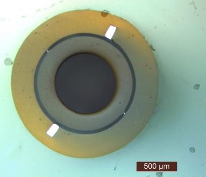
2 Research at FIMAP Interplay between the viscous flow and intermolecular forces to integrate complex functionalities within unconventional substrates - Multi-material nanostructured 2D and 3D coatings 500nm - Multi-material 1D fibre devices 2


3 OPTICAL FIBERS Professor Kao received the Nobel Prize in Physics in 2009 for the development of optical fibers Glasses have low optical losses AND can be processed efficiently into fibers From optical fibres. Optical transport Sensing and monitoring. to a unique materials processing opportunity Thermal drawing process Simple, scalable, low-cost Unique micro-structures Distributed functionality Flexibility 3


4 A Fantastic Materials Processing Technique Photonic devices require an index contrast Langmuir 27, Different materials with different optical and thermo-mechanical properties Xue et. al. J. Light Wave 2004 Effects of surface tension (the process generates surface area) A rich material process Extremely fine structures over extended flexible lengths Nature 420, 650 (2002) 4


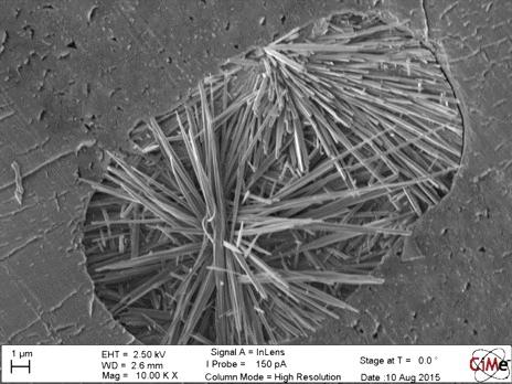
5 Multi-material Fiber paradigm Engineering novel 1D nanostructured devices Conventional fibers Materials Structure Length scale Manufacturing on the preform level Heat and draw down - 1 m long, 300 mm in diameter preform pulled into tens-of-kilometer long fiber - Such fiber would cover 10 to 100 square meters!! Single material Simple geometry Large feature sizes 200µm Extended length of functional fibers 5


 Adv.")
6 In-fiber metallic systems Canales et. al., Nature Biotechnology (2015) Bayindir, Sorin et. al. Nature 431, 826 (2004) Adv. Optical Materials 1, 971 (2013)
7 MATERIALS SELECTION HIGH-Tg TERMOPLASTICS O S O O n Electrical Insulators PES, PEI Amorphous thermoplastics Glass transition temperature: o C Refractive microns: 1.6 Availability: Thin films (8-150 microns) AMORPHOUS SEMICONDUCTORS Amorphous semiconductors (p-type) Glass transition temperature: o C As, Se, S, Ge, Te, Si, Sn Refractive microns: High electrical conductivity CTE for As2Se3: 25*10^-6/C Photoconductivity Sb Chalcogens S METALS In, Sn, Bi(43%)-Sn(57%) Metals Crystalline Materials Melting Temperature: o C T m has to be lower than the drawing temperature Good wetting of glass and polymer Use of Flux to prevent oxidization Low viscosity at drawing Temperature As Ge Ga Se Te 7


8 Metal-Insulator-Semiconductor fiber Draw-tower Preform cross section Fiber cross section The thermal drawing process inherently generates surface area! M. Bayindir, F. Sorin, et al Nature 431, 826 (2004) 8


9 OPTOELECRONIC FIBER SENSORS We have already made a photoconductor V A I-V Curve R Extremely large area flexible optoelectronic devices Can we integrate increasingly complex and innovative device structures? M. Bayindir, F. Sorin, et al Nature 431, 826 (2004)


 F.")
10 THIN-FILM FIBER DEVICES A change of architecture can lead to significant improvement in performance Semiconductor PES 1 µm PES Sn SENSITIVITY vs PENETRATION DEPTH PHOTOCURRENT RATIO vs WAVELENGTH F. Sorin et al, Advanced Materials, 19(22) pp (2007) F. Sorin et al, NanoLetters 9 (7), pp (2009). 10


11 HEALTH CARE APPLICATION Distributed heat sensing for safety monitoring OmniGuide CO 2 Laser Beam Delivery System for non-invasive surgery Thermal Sensor (Patent licensed by Omniguide Inc) 11

and)electrochemical)applications) mbled)materials)with)electron)microscopy!")
12 Microfluidic transverse fiber lasers inar! - We demonstrated surface emitting fiber lasers - Using our multimaterial fiber platform, we could add liquid crystal filled channels or)nanomedicine)applications) - Another example of integration of complex and different functionalities. c)and)electrochemical)applications) mbled)materials)with)electron)microscopy!! rticles)to)aerogels)and)metallic)foams) e)resistant)cement! otonic@plasmonic)coupling)on)planar)chips) 12 A. Stolyarov, et al, Nature Photonics, (2012)


13 Microfluidic transverse fiber lasers Directional light based activation of photosensitive compounds. A. Stolyarov, et al, Nature Photonics, (2012) 13


14 Fiber-integrated Nanowire based detectors PMMA Polycarbonate SnZn metal Polysulfone Semiconductor Conducting nanocomposite 14


15 RESEARCH AT FIMAP Advanced multi-material optical and optoelectronic fibers Microstructured and microtextured fibers and fabrics Template dewetting of novel materials for Photonic devices Research areas Novel materials for innovative biocompatible, degradable and stretchable fibers Novel planar and fiber devices fiber assemblies Planar and fiber systems characterization Process and Photonic properties modeling Dynamic flow of viscous liquids and thin films / Surface and interface science and engineering / Innovative device architectures Template dewetting Thermal drawing


16 Group and sponsors FIMAP today: Wei Yann PhD student Tapajyoti Das Gupta Postdoc Anne Roy Amdinistration DangTung Nguyen PhD student Yunpeng Qu Postdoc Alexis Page PhD student Marco Volpi PhD student Chie Kitano Postdoc Acknowledgment: - Prof. Fink and Prof. Joannopoulos - All the collaborators at MIT: Prof. Abouraddy, Dr. Lei Wei, Prof. Zheng Wang, Dr. Shapira, Dr. Stolyarov, Dr. Danto, Dr. Hart, etc Sponsors:
nanomedicine)applications)")


17 inar! THANK YOU or)nanomedicine)applications) c)and)electrochemical)applications) mbled)materials)with)electron)microscopy!! rticles)to)aerogels)and)metallic)foams) e)resistant)cement!
High Pressure Chemical Vapor Deposition to make Multimaterial Optical Fibers
 High Pressure Chemical Vapor Deposition to make Multimaterial Optical Fibers Subhasis Chaudhuri *1 1, 2, 3, John V. Badding 1 Department of Chemistry, Pennsylvania State University, University Park, PA
EXCIMER LASER ANNEALING FOR LOW- TEMPERATURE POLYSILICON THIN FILM TRANSISTOR FABRICATION ON PLASTIC SUBSTRATES
 EXCIMER LASER ANNEALING FOR LOW- TEMPERATURE POLYSILICON THIN FILM TRANSISTOR FABRICATION ON PLASTIC SUBSTRATES G. Fortunato, A. Pecora, L. Maiolo, M. Cuscunà, D. Simeone, A. Minotti, and L. Mariucci CNR-IMM,
TEMPERATURE-DEPENDENT REFRACTIVE INDICES OF OPTICAL PLANAR WAVEGUIDES
 TEMPERATURE-DEPENDENT REFRACTIVE INDICES OF OPTICAL PLANAR WAVEGUIDES Aiman Kassir a, Abang Annuar Ehsan b, Noraspalelawati Razali b, Mohd Kamil Abd Rahman a and Sahbudin Shaari b Faculty of Applied Sciences,
High precise welding of transparent polymers
 Lasers in Manufacturing Conference 2015 High precise welding of transparent polymers Frederick Vinzent a *, Michael Schwalme a, Tobias Jaus a, Manuel Sieben a a LPKF Laser & Electronics AG, Alfred-Nobel-Straße
Electronics from the Printing Press
 Electronics from the Printing Press Hannover Messe 2011 April 4 8, 2011, Hannover Research & Technology Leading Trade Fair for R & D and Technology Transfer Hall 2, Booth C18 Research Teaching Innovation
NanoSystemsEngineering: NanoNose Final Status, March 2011
 1 NanoSystemsEngineering: NanoNose Final Status, March 2011 The Nanonose project is based on four research projects (VCSELs, 3D nanolithography, coatings and system integration). Below, the major achievements
Silver Diffusion Bonding and Layer Transfer of Lithium Niobate to Silicon
 Chapter 5 Silver Diffusion Bonding and Layer Transfer of Lithium Niobate to Silicon 5.1 Introduction In this chapter, we discuss a method of metallic bonding between two deposited silver layers. A diffusion
Bridging Nanoscience and Manufacturing
 Bridging Nanoscience and Manufacturing Xiaochun Li Professor and Raytheon Chair in Manufacturing Department of Mechanical and Aeropsace Engineering UCLA Bridging Nanoscience and Manufacturing Penetration
Workshop on Nanoscience and Catalysts March 2008, QAU, Islamabad Nanocomposites for Thermal management Applications
 Fazal Ahmad Khalid Pro-Rector GIK Institute of Engineering Sciences and Technology Topi, NWFP, Pakistan (Khalid@giki.edu.pk) Workshop on Nanoscience and Catalysts 24-25 March 2008, QAU, Islamabad Nanocomposites
Scintillating Optical Fibers
 Scintillating Optical Fibers Plastic Scintillating Fibers Saint-Gobain Crystals manufactures a variety of plastic scintillating, wavelength-shifting and light-transmitting fibers used for research and
International Journal of Scientific & Engineering Research, Volume 6, Issue 2, February-2015 ISSN PHOTONIC CRYSTAL FIBER- AN OVERVIEW
 45 PHOTONIC CRYSTAL FIBER- AN OVERVIEW Neha Mahnot1, Shikha Maheshwary2, Rekha Mehra3 1, 2, 3 Govt. Engg. College, Ajmer 2 shikhasm1992@gmail.com 1 neha29mahnot@gmail.com Abstract- This review paper gives
Nanoimprinting in Polymers and Applications in Cell Studies. Albert F. YEE Chemical Engineering & Materials Science UC Irvine
 Nanoimprinting in Polymers and Applications in Cell Studies Albert F. YEE Chemical Engineering & Materials Science UC Irvine Presentation outline Motivation Reversal imprinting Soft inkpad imprinting on
Fraunhofer ENAS Current results and future approaches in Wafer-level-packaging FRANK ROSCHER
 Fraunhofer ENAS - Current results and future approaches in Wafer-level-packaging FRANK ROSCHER Fraunhofer ENAS Chemnitz System Packaging Page 1 System Packaging Outline: Wafer level packaging for MEMS
Micro and nano structuring of carbon based materials for micro injection moulding and hot embossing
 Micro and nano structuring of carbon based materials for micro injection moulding and hot embossing Victor Usov, Graham Cross, Neal O Hara, Declan Scanlan, Sander Paulen, Chris de Ruijter, Daniel Vlasveld,
Mater. Res. Soc. Symp. Proc. Vol Materials Research Society
 Mater. Res. Soc. Symp. Proc. Vol. 940 2006 Materials Research Society 0940-P13-12 A Novel Fabrication Technique for Developing Metal Nanodroplet Arrays Christopher Edgar, Chad Johns, and M. Saif Islam
Laser Welding of Engineering Plastics
 Laser Welding of Engineering Plastics Technical Information Further information on individual products: www.ultramid.de www.ultradur-lux.basf.com www.ultrason.de www.plasticsportal.eu/ultraform 2 LASER
Experiences of PLD Technology for LIB Separators. PICODEON Oy. Neal White
 Experiences of PLD Technology for LIB Separators PICODEON Oy Neal White 1 Outline Introduction to Picodeon Ceramic coating rationale Separator overview Why PLD for LIB separators Current status of Picodeon
Light Trapping Enhancement in Thin Film Silicon Solar Cell with Different Back Reflector
 International Journal of Electrical Components and Energy Conversion 2017; 3(5): 83-87 http://www.sciencepublishinggroup.com/j/ijecec doi: 10.11648/j.ijecec.20170305.11 ISSN: 2469-8040 (Print); ISSN: 2469-8059
Chapter 3 Silicon Device Fabrication Technology
 Chapter 3 Silicon Device Fabrication Technology Over 10 15 transistors (or 100,000 for every person in the world) are manufactured every year. VLSI (Very Large Scale Integration) ULSI (Ultra Large Scale
Polymer-based optical interconnects using nano-imprint lithography
 Polymer-based optical interconnects using nano-imprint lithography Arjen Boersma,Sjoukje Wiegersma Bert Jan Offrein, Jeroen Duis, Jos Delis, Markus Ortsiefer, Geert van Steenberge, MikkoKarppinen, Alfons
White Paper: Pixelligent Internal Light Extraction Layer for OLED Lighting
 White Paper: Pixelligent Internal Light Zhiyun (Gene) Chen, Ph.D., Vice President of Engineering Jian Wang, Ph.D., Manager, Application Engineering Pixelligent Technologies LLC, 6411 Beckley Street, Baltimore,
Kinetic Analysis of Crystallization Processes in In 60 Se 40 Thin Films for Phase Change Memory (Pram) Applications
 Applications") Advances in Materials 2016; 5(4): 18-22 http://www.sciencepublishinggroup.com/j/am doi: 10.11648/j.am.20160504.11 ISSN: 2327-2503 (Print); ISSN: 2327-252X (Online) Kinetic Analysis of Crystallization Processes
Advances in Materials 2016; 5(4): 18-22 http://www.sciencepublishinggroup.com/j/am doi: 10.11648/j.am.20160504.11 ISSN: 2327-2503 (Print); ISSN: 2327-252X (Online) Kinetic Analysis of Crystallization Processes
Temperature Stability of RF Components R. Akre 4/21/2005
 Temperature Stability of RF Components R. Akre 4/21/2005 Typically the phase change of the RF passing through a device will change with temperature. With near speed of light cables, the cable length increases
APPLICATIONS OF CHALCOGENIDE GLASS BULKS AND FIBRES
 Journal of Optoelectronics and Advanced Materials Vol. 5, No. 5, 2003, p. 1327-1333 Invited Paper APPLICATIONS OF CHALCOGENIDE GLASS BULKS AND FIBRES X. Zhang *, H. Ma, J. Lucas UMR CNRS 6512 "Verres et
11.3 Polishing with Laser Radiation
 196 E. Willenborg 11.3 Polishing with Laser Radiation Edgar Willenborg The surface roughness of a part or product strongly influences its properties and functions. Among these can be counted abrasion and
12.0 Materials for Missile, Space, and Launch Systems
 12.0 Materials for Missile, Space, and Launch Systems 12.1 Introduction Affordability is the key criterion for assessing the value of a new technology and its potential incorporation into military applications.
Micro Laser Assisted Machining (µ-lam) of Semiconductors and Ceramics. Machining Direction
 of Semiconductors and Ceramics. Machining Direction") Micro Laser Assisted Machining (µ-lam) of Semiconductors and Ceramics John Patten, Director, Manufacturing Research Center Western Michigan University Machining Direction IR laser Machining Direction Work
Micro Laser Assisted Machining (µ-lam) of Semiconductors and Ceramics John Patten, Director, Manufacturing Research Center Western Michigan University Machining Direction IR laser Machining Direction Work
3D Laser Lithography in Biotechnology and Medical Technology
 3D Laser Lithography in Biotechnology and Medical Technology High-Precision, Piezo-Based Nanopositioning Systems Advance Technology Page 1 of 6 Laser technology makes it possible to create even very complex
Manufacturing of fibre preforms with granulated oxides: Influence of the grain size
 PART III 1 Manufacturing of fibre preforms with granulated oxides: Influence of the grain size R. Scheidegger, L. Di Labio, W. Lüthy, T. Feurer Institute of Applied Physics, University of Bern, Sidlerstrasse
Semiconductor Technology
 Semiconductor Technology from A to Z Oxidation www.halbleiter.org Contents Contents List of Figures List of Tables II III 1 Oxidation 1 1.1 Overview..................................... 1 1.1.1 Application...............................
Trench Structure Improvement of Thermo-Optic Waveguides
 International Journal of Applied Science and Engineering 2007. 5, 1: 1-5 Trench Structure Improvement of Thermo-Optic Waveguides Fang-Lin Chao * Chaoyang University of Technology, Wufong, Taichung County
Radiation Tolerant Isolation Technology
 Radiation Tolerant Isolation Technology Background The following contains a brief description of isolation technologies used for radiation hardened integrated circuits. The technologies mentioned are junction
Introduction to Micro/Nano Fabrication Techniques. Date: 2015/05/22 Dr. Yi-Chung Tung. Fabrication of Nanomaterials
 Introduction to Micro/Nano Fabrication Techniques Date: 2015/05/22 Dr. Yi-Chung Tung Fabrication of Nanomaterials Top-Down Approach Begin with bulk materials that are reduced into nanoscale materials Ex:
A COMPARISON OF THE TRANSMISSION LOSSES OF DIFFERENT OPTICAL FIBER MATERIALS
 PK ISSN 22-2941; CODEN JNSMAC Vol. 46, No.1 & 2 (April & October 26) PP 47-51 A COMPARISON OF THE TRANSMISSION LOSSES OF DIFFERENT OPTICAL FIBER MATERIALS S F SHAUKAT, M A U KHAN, R FAROOQ* Department
Preprint - Mechatronics 2008, Le Grand-Bornand, France, May
 Potentialities of piezoresistive cantilever force sensors based on free standing thick films Hélène Debéda(*), Isabelle Dufour, Patrick Ginet, Claude Lucat University of Bordeaux 1, IMS Laboratory, 51
Confocal Microscopy of Electronic Devices. James Saczuk. Consumer Optical Electronics EE594 02/22/2000
 Confocal Microscopy of Electronic Devices James Saczuk Consumer Optical Electronics EE594 02/22/2000 Introduction! Review of confocal principles! Why is CM used to examine electronics?! Several methods
FABRICATION ENGINEERING MICRO- NANOSCALE ATTHE AND. Fourth Edition STEPHEN A. CAMPBELL. of Minnesota. University OXFORD UNIVERSITY PRESS
 AND FABRICATION ENGINEERING ATTHE MICRO- NANOSCALE Fourth Edition STEPHEN A. CAMPBELL University of Minnesota New York Oxford OXFORD UNIVERSITY PRESS CONTENTS Preface xiii prrt i OVERVIEW AND MATERIALS
Plastic Coated Silica/Silica (Low OH) FIBER CROSS SECTION Polyimide and Acrylate Coated. Nylon and Tefzel Coated
 FIBER CROSS SECTION Polyimide and Acrylate Coated. Nylon and Tefzel Coated") DESCRIPTION When looking for a high quality fiber with superior transmission and a numerical aperture (N.A.) of 0.22 for efficient light coupling, the is the fiber of choice. The Anhydroguide fiber is
DESCRIPTION When looking for a high quality fiber with superior transmission and a numerical aperture (N.A.) of 0.22 for efficient light coupling, the is the fiber of choice. The Anhydroguide fiber is
Nanophotonics: principle and application. Khai Q. Le Lecture 11 Optical biosensors
 Nanophotonics: principle and application Khai Q. Le Lecture 11 Optical biosensors Outline Biosensors: Introduction Optical Biosensors Label-Free Biosensor: Ringresonator Theory Measurements: Bulk sensing
A new Glass GEM with a single sided guard-ring structure
 A new Glass GEM with a single sided guard-ring structure RD-51 session! 5 July, 2013!! Yuki MITSUYA a, Takeshi FUJIWARA b, Hiroyuki TAKAHASHI a!! a Department of Nuclear Engineering and Management, The
LASER MICROMACHINING A New Tool for Precision Engineers
 LASER MICROMACHINING A New Tool for Precision Engineers Nadeem Rizvi UK Laser Micromachining Centre Laser Applications for Micro and Nano Engineering AILU Workshop 14 June 2006 (Oxford) FOCUS ON MICRO
Corning RC Specialty Fibers Reduced Cladding Fibers Enable Miniaturization and Device Integration
 Corning RC Specialty Fibers Reduced Cladding Fibers Enable Miniaturization and Device Integration Photonic Materials PI1442 Issued: July 2005 Supersedes: August 2003 Featuring ultra-tight specifications,
Die Attach Materials. Die Attach G, TECH. 2U. TECHNICAL R&D DIV.
 Die Attach Materials Die Attach G, TECH. 2U. TECHNICAL R&D DIV. 2 Topics 3 What it is X 5,000 X 10,000 X 50,000 Si Chip Au Plating Substrate Ag Resin 4 Current Products Characteristics H9890-6A H9890-6S
MI USA. 1, Eggenstein-Leopoldshafen, Germany. Engineering, University of Michigan, Ann Arbor, MI USA
 Evaluating UV/H 2 O 2 Exposure as a DEHP Degradation Treatment for Plasticized PVC Jeanne M. Hankett 1, Alexander Welle 2,3, Joerg Lahann 4, Zhan Chen 1 * 1 Department of Chemistry, University of Michigan,
3. Overview of Microfabrication Techniques
 3. Overview of Microfabrication Techniques The Si revolution First Transistor Bell Labs (1947) Si integrated circuits Texas Instruments (~1960) Modern ICs More? Check out: http://www.pbs.org/transistor/background1/events/miraclemo.html
EXTRUSION OF ELASTOMER FILM, EFFECTS OF ELASTOMER DESIGN ON CHILL ROLL STICKING
 EXTRUSION OF ELASTOMER FILM, EFFECTS OF ELASTOMER DESIGN ON CHILL ROLL STICKING Mary Ann Jones, Todd Hogan, and Sarah Gassner, The Dow Chemical Company, Midland, MI Abstract Sticking of plastic webs to
BASF Corporation. Abstract. Introduction. Basic Principles for LW of Thermoplastics. Non-Contact Laser Welding (NCLW)
") BASF Corporation FORWARD TO BETTER UNDERSTANDING OF OPTICAL CHARACTERIZATION AND DEVELOPMENT OF COLORED POLYAMIDES FOR THE INFRA-RED/LASER WELDING: PART I EFFICIENCY OF POLYAMIDES FOR INFRA-RED WELDING
BASF Corporation FORWARD TO BETTER UNDERSTANDING OF OPTICAL CHARACTERIZATION AND DEVELOPMENT OF COLORED POLYAMIDES FOR THE INFRA-RED/LASER WELDING: PART I EFFICIENCY OF POLYAMIDES FOR INFRA-RED WELDING
Optical fibers. Laboratory of optical fibers. Institute of Photonics and Electronics AS CR, v.v.i.
 Optical fibers Laboratory of optical fibers Institute of Photonics and Electronics AS CR, v.v.i. http://www.ufe.cz/en/laboratory-optical-fibres n 1 n 1 > n 2 Waveguiding principle optical fiber W. Snell
Optical and Photonic Glasses. Lecture 4. Glass Composition and Preparations. Professor Rui Almeida
 Optical and Photonic Glasses : Glass Composition and Preparations Professor Rui Almeida International Materials Institute For New Functionality in Glass Lehigh University For a given, selected value of
Optical Fiber Sensors for Biomedical Applications
 Optical Fiber Sensors for Biomedical Applications Xingwei (Vivian) Wang, Ph.D. Assistant Professor Department of Electrical and Computer Engineering University of Massachusetts Lowell Phone: (978) 934-1981
Hard Coated Silica/Silica (Low OH) Radius
 Radius") DESCRIPTION When looking for a silica core and silica clad fiber with a hard polymer coating that allows a high core-to-clad ratio and a numerical aperture (N.A.) of 0.22 for efficient light coupling,
DESCRIPTION When looking for a silica core and silica clad fiber with a hard polymer coating that allows a high core-to-clad ratio and a numerical aperture (N.A.) of 0.22 for efficient light coupling,
TGV and Integrated Electronics
 TGV and Integrated Electronics Shin Takahashi ASAHI GLASS CO., LTD. 1 Ambient Intelligence Green Energy/Environment Smart Factory Smart Mobility Smart Mobile Devices Bio/Medical Security/Biometrics 2 Glass
Application Note #124 VITA: Quantitative Nanoscale Characterization and Unambiguous Material Identification for Polymers
 Local thermal analysis identifies polymer AFM image of polymer blend Application Note #124 VITA: Quantitative Nanoscale Characterization and Unambiguous Material Identification for Polymers VITA module
Micophotometric Control of Particles and Inhomogeneities in Flowing Polymer Melts during Extrusion Processing
 M.Stephan, S.Große: Micophotometric Control of Particles and Inhomogeneities in Flowing Polymer Melts during Extrusion Processing Workshop January, 28 th -29 th 2005, Dresden Particulate Heterogeneities
LOT. Contents. Introduction to Thin Film Technology. Chair of Surface and Materials Technology
 Introduction to Thin Film Contents 1. Introduction and Application Examples (2h) 2. Preparation of Thin Films by PVD (Physical Vapor Deposition) (6h) 2.1 Vacuum Technique (1h) 2.1.1 Kinetics of Gases 2.1.2
Development of Piezoelectric Nanocomposites for Energy Harvesting and Self-Sensing
 Development of Piezoelectric Nanocomposites for Energy Harvesting and Self- Kenneth J. Loh Assistant Professor Department of Civil & Environmental Engineering University of California, Davis The Applied
LASER MICROPROCESSING POWERED BY UV PHOTONS Paper #P109
 LASER MICROPROCESSING POWERED BY UV PHOTONS Paper #P109 Ralph Delmdahl, Rainer Paetzel Coherent GmbH, Hans-Boeckler-Str.12, Goettingen, 37079, Germany Abstract Lasers with ultraviolet (UV) output offer
Ceramic materials with submicron structure based on nanopowders
 Ceramic materials with submicron structure based on nanopowders Uwe Reichel, Fraunhofer Institute for Ceramic Technologies and Systems IKTS Institutsteil Hermsdorf, D-07629 Hermsdorf, Germany Nanophotonics
Free standing Multilayer Thin Film of Cellulose Nanocrystals
 Free standing Multilayer Thin Film of Cellulose Nanocrystals Chaoyang Jiang Department of Chemistry The University of South Dakota Edmonton, June 25, 2009 Cellulose Nanocrystals Nanotechnology R&D Priority
Reactive molten core fabrication of silicon optical fiber
 Reactive molten core fabrication of silicon optical fiber S. Morris, 1,2 T. Hawkins, 1,2 P. Foy, 1,2 C. McMillen, 1,3 J. Fan, 1,4 L. Zhu, 1,4 R. Stolen, 1,2 R. Rice, 5 and J. Ballato 1,2,4,* 1 Center for
Plasmonics using Metal Nanoparticles. Tammy K. Lee and Parama Pal ECE 580 Nano-Electro-Opto-Bio
 Plasmonics using Metal Nanoparticles Tammy K. Lee and Parama Pal ECE 580 Nano-Electro-Opto-Bio April 1, 2007 Motivation Why study plasmonics? Miniaturization of optics and photonics to subwavelength scales
ELECTROSPUN EVOH FIBRES REINFORCED WITH BACTERIAL CELLULOSE NANOWHISKERS WITH POTENTIAL IN FOOD PACKAGING APPLICATIONS
 ELECTROSPUN EVOH FIBRES REINFORCED WITH BACTERIAL CELLULOSE NANOWHISKERS WITH POTENTIAL IN FOOD PACKAGING APPLICATIONS Novel Materials and Nanotechnology Group Marta Martínez-Sanz Richard T. Olsson Amparo
Obviously the type of product or coating required will determine the surface required & technique to produce it.
 Etching & texturing polymer films - different options for patterned deposition or encouraging nucleation. Charles A. Bishop C.A.Bishop Consulting Ltd. Abstract. A number of the nanotechnologies or psuedonanotechnologies
Fabrication of Mg2Si pn-junction Photodiode with Shallow Mesa-structure and Ring Electrode
 Proc. Asia-Pacific Conf. on Semiconducting Silicides and Related Materials 2016 JJAP Conf. Proc. 5, https://doi.org/10.7567/jjapcp.5.011102 Fabrication of Mg2Si pn-junction Photodiode with Shallow Mesa-structure
D Eggenstein-Leopoldshafen, Germany 2 University of Karlsruhe (TH), Institute for Microstructure Technology (IMT),
, Institute for Microstructure Technology (IMT),") Sub-µ structured Lotus Surfaces Manufacturing M. Worgull 1, M. Heckele 1, T. Mappes 2, B. Matthis 1, G. Tosello 3, T. Metz 4, J. Gavillet 5, P. Koltay 4, H. N. Hansen 3 1 Forschungszentrum Karlsruhe (FZK),
Sub-µ structured Lotus Surfaces Manufacturing M. Worgull 1, M. Heckele 1, T. Mappes 2, B. Matthis 1, G. Tosello 3, T. Metz 4, J. Gavillet 5, P. Koltay 4, H. N. Hansen 3 1 Forschungszentrum Karlsruhe (FZK),
Optical and Photonic Glasses. Lecture 21. Abnormal Dispersion and Athermal Glasses. Professor Rui Almeida
 Optical and Photonic Glasses : Abnormal Dispersion and Athermal Glasses Professor Rui Almeida International Materials Institute For New Functionality in Glass Lehigh University Abnormal dispersion and
Sustainable UV-curable low refractive index resins with novel polymers for polymer cladding materials
 Sustainable UV-curable low refractive index resins with novel polymers for polymer cladding materials Hiroki Tokoro*, Takako Ishikawa, Nobuyuki Koike, Yohzoh Yamashina DIC Corporation, 12 Yawatakaigan-dori,
Tackling the optical interconnection challenge for the Integrated Photonics Revolution
 Tackling the optical interconnection challenge for the Integrated Photonics Revolution Dr. Ir. TU Delft, Precision and Microsystems Engineering m.tichem@tudelft.nl Microfabrication and MEMS Si microfabrication
Challenges and Future Directions of Laser Fuse Processing in Memory Repair
 Challenges and Future Directions of Laser Fuse Processing in Memory Repair Bo Gu, * T. Coughlin, B. Maxwell, J. Griffiths, J. Lee, J. Cordingley, S. Johnson, E. Karagiannis, J. Ehrmann GSI Lumonics, Inc.
Nanostructured Engineered Materials With High Magneto-optic Performance For Integrated Photonics Applications
 Edith Cowan University Research Online School of Engineering Publications 28 Nanostructured Engineered Materials With High Magneto-optic Performance For Integrated Photonics Applications Mikhail Vasiliev
UNCLASSIFIED/UNLIMITED. Ultrasonic Consolidation : Status Report on Development of Solid State Net Shape Processing for Direct Manufacturing
 of Solid State Net Shape Processing for Direct Manufacturing ABSTRACT Dr. Dawn R. White Solidica, Inc. 3941 Research Park Drive, Ste. C Ann Arbor, MI 48108 USA dawn@solidica.com Ultrasonic Consolidation
Axially Graded Index Lens (AGILE) as a non-tracking solar concentrator
 as a non-tracking solar concentrator") Axially Graded Index Lens (AGILE) as a non-tracking solar concentrator Investigators Olav Solgaard, Associate Professor, Electrical Engineering; Reinhold Dauskardt, Professor, Material Sciences and Engineering;
Axially Graded Index Lens (AGILE) as a non-tracking solar concentrator Investigators Olav Solgaard, Associate Professor, Electrical Engineering; Reinhold Dauskardt, Professor, Material Sciences and Engineering;
PULSED LASER WELDING
 PULSED LASER WELDING Girish P. Kelkar, Ph.D. Girish Kelkar, Ph.D, WJM Technologies, Cerritos, CA 90703, USA Laser welding is finding growing acceptance in field of manufacturing as price of lasers have
Three-Dimensional Laser Writing on the Nanometer Scale
 Three-Dimensional Laser Writing on the Nanometer Scale Piezo Drives are Driving Technology Forward Page 1 of 5 The best possible positioning accuracy is now mandatory in many fields of application. The
Coatings. Ion Assisted Deposition (IAD) process Advance Plasma Source (APS) plasma-ion assisted Deposition. Coatings on Optical Fibers
 process Advance Plasma Source (APS) plasma-ion assisted Deposition. Coatings on Optical Fibers") Anti-Reflection Custom Ion Assisted Deposition (IAD) process Advance Plasma Source (APS) plasma-ion assisted Deposition Anti-Reflection on Optical Fibers OptoSigma supplies a wide selection of optical
Anti-Reflection Custom Ion Assisted Deposition (IAD) process Advance Plasma Source (APS) plasma-ion assisted Deposition Anti-Reflection on Optical Fibers OptoSigma supplies a wide selection of optical
Amorphous silicon waveguides for microphotonics
 4 Amorphous silicon waveguides for microphotonics Amorphous silicon a-si was made by ion irradiation of crystalline silicon with 1 10 15 Xe ions cm 2 at 77 K in the 1 4 MeV energy range. Thermal relaxation
The Electronics Biological Matter Interface.
 The Electronics Biological Matter Interface. Introduction. The interface of inorganic materials and biological matter is a subject of significant current interest. The fundamental science of this area
Preparation and characterization of nanostructured thermoelectric materials
 QuickTime et un décompresseur TIFF (non compressé) sont requis pour visionner cette image. Preparation and characterization of nanostructured thermoelectric materials Laboratoire de Physique des Matériaux,
Substrate surface effect on the structure of cubic BN thin films from synchrotron-based X-ray diffraction and reflection
 Substrate surface effect on the structure of cubic BN thin films from synchrotron-based X-ray diffraction and reflection X.M. Zhang, W. Wen, X.L.Li, X.T. Zhou published on Dec 2012 PHYS 570 Instructor
Thermal response of Bragg gratings in PMMA microstructured optical fibers
 Thermal response of Bragg gratings in PMMA microstructured optical fibers Karen E Carroll 1*, Chi Zhang 1, David J. Webb 1, Kyriacos Kalli 2, Alexander Argyros 3, Maryanne C. J. Large 3 1 Photonics Research
Optical and Photonic Glasses. Lecture 1. Intro to Glass and the Glass Transition. Professor Rui Almeida
 Optical and Photonic Glasses : Intro to Glass and the Glass Transition Professor Rui Almeida International Materials Institute For New Functionality in Glass Lehigh University Program Glass and amorphous
EECS130 Integrated Circuit Devices
 EECS130 Integrated Circuit Devices Professor Ali Javey 9/13/2007 Fabrication Technology Lecture 1 Silicon Device Fabrication Technology Over 10 15 transistors (or 100,000 for every person in the world)
1. INTRODUCTION. (a) Sand/ Fabric-coated (b) Sand-coated deformed. (c) Helical wrapped/ribbed Fig.1 FRP anchors with different outer surfaces
 Sand/ Fabric-coated (b) Sand-coated deformed. (c) Helical wrapped/ribbed Fig.1 FRP anchors with different outer surfaces") S2B3 Interface Bond Strength of Helical Wrapped GFRP Ground Anchors Weichen Xue Prof., Department of Building Engineering, Tongji University, Shanghai, China Yuan Tan PhD candidate, Department of Building
S2B3 Interface Bond Strength of Helical Wrapped GFRP Ground Anchors Weichen Xue Prof., Department of Building Engineering, Tongji University, Shanghai, China Yuan Tan PhD candidate, Department of Building
Laser printing of organic lightemitting diode pixels by LIFT. James Shaw-Stewart
 Laser printing of organic lightemitting diode pixels by LIFT James Shaw-Stewart Optimising the fabrication of OLEDs by laser-induced forward transfer Functional Thin Films 16th October 2014 James Shaw-Stewart
Aerospace and Automotive Seat Frames from Carbon and PPS Thermoplastic Tape. Bob Newill Ticona Engineering Polymers
 Aerospace and Automotive Seat Frames from Carbon and PPS Thermoplastic Tape Bob Newill Ticona Engineering Polymers 1 Outline Background Aerospace and Automotive Seat Frames Trends Supporting Change Composites
Through Silicon Vias Annealing: A thermo-mechanical assessment
 Dresden University of Technology / Through Silicon Vias Annealing: P. Saettler (1), K. J. Wolter (1), M. Hecker (2), M. Boettcher (3) and C. Rudolph (3) (1) Technische Universität Dresden, (2) Globalfoundries
NON-PLANAR SILICON OXIDATION: AN EXTENSION OF THE DEAL-GROVE MODEL BRIAN D. LEMME. B.S., University of Nebraska-Lincoln, 2000 A REPORT
 NON-PLANAR SILICON OXIDATION: AN EXTENSION OF THE DEAL-GROVE MODEL by BRIAN D. LEMME B.S., University of Nebraska-Lincoln, 2000 A REPORT submitted in partial fulfillment of the requirements for the degree
Laser printing and curing/sintering of silver paste lines for solar cell metallization
 Lasers in Manufacturing Conference 2015 Laser printing and curing/sintering of silver paste lines for solar cell metallization D. Munoz-Martin a *, Y. Chen a, A. Márquez a, M. Morales a, C. Molpeceres
In-Situ Monitoring of Pattern Filling in Nano-Imprint Lithography Using Surface Plasmon Resonance
 Copyright 2011 American Scientific Publishers All rights reserved Printed in the United States of America Journal of Nanoscience and Nanotechnology Vol. 11, 1 6, 2011 In-Situ Monitoring of Pattern Filling
Specimen Preparation Technique for a Microstructure Analysis Using the Focused Ion Beam Process
 Specimen Preparation Technique for a Microstructure Analysis Using the Focused Ion Beam Process by Kozue Yabusaki * and Hirokazu Sasaki * In recent years the FIB technique has been widely used for specimen
BBO Crystals. Features. Broad phase-matchable second-harmonic-generation (SHG) range from nm to 2500 nm
 range from nm to 2500 nm") BBO Crystals Broad phase-matchable second-harmonic-generation (SHG) range from 409.6 nm to 2500 nm Wide transparency range from 189 nm to 2600 nm High damage threshold of 10 J/cm 2 for 10 ns pulse-width
BBO Crystals Broad phase-matchable second-harmonic-generation (SHG) range from 409.6 nm to 2500 nm Wide transparency range from 189 nm to 2600 nm High damage threshold of 10 J/cm 2 for 10 ns pulse-width
Woven Electrodes for Optoelectronic Devices. Peter Chabrecek. Sefar AG, 9425 Thal, Switzerland
 Peter Chabrecek Sefar AG, 9425 Thal, Switzerland Actual SEFAR business Sefar's core skills is the manufacture and market of fabrics with precise mesh openings for screen printing and filtration processes
Heat Transfer in Polymers
 Heat Transfer in Polymers Martin Rides, Angela Dawson 6 October 2004 Heat Transfer in Polymers - summary Introduction Heat Transfer Coefficient Thermal Conductivity Industrial Demonstrations NPL s Polymer
Micro processing with laser radiation
 Micro processing with laser radiation Trends and perspectives Miniaturization and highly integrated functionalization are the driving factors in the production of innovative products in almost every industrial
1. Introduction. What is implantation? Advantages
 Ion implantation Contents 1. Introduction 2. Ion range 3. implantation profiles 4. ion channeling 5. ion implantation-induced damage 6. annealing behavior of the damage 7. process consideration 8. comparison
3.46 OPTICAL AND OPTOELECTRONIC MATERIALS
 Badgap Engineering: Precise Control of Emission Wavelength Wavelength Division Multiplexing Fiber Transmission Window Optical Amplification Spectrum Design and Fabrication of emitters and detectors Composition
Yung-Hui Yeh, and Bo-Cheng Kung Display Technology Center (DTC), Industrial Technology Research Institute, Hsinchu 310, Taiwan
, Industrial Technology Research Institute, Hsinchu 310, Taiwan") Amorphous In 2 O 3 -Ga 2 O 3 -ZnO Thin Film Transistors and Integrated Circuits on Flexible and Colorless Polyimide Substrates Hsing-Hung Hsieh, and Chung-Chih Wu* Graduate Institute of Electronics Engineering,
Amorphous In 2 O 3 -Ga 2 O 3 -ZnO Thin Film Transistors and Integrated Circuits on Flexible and Colorless Polyimide Substrates Hsing-Hung Hsieh, and Chung-Chih Wu* Graduate Institute of Electronics Engineering,
Lecture 7 CMOS MEMS. CMOS MEMS Processes. CMOS MEMS Processes. Why CMOS-MEMS? Agenda: CMOS MEMS: Fabrication. MEMS structures can be made
 EEL6935 Advanced MEMS (Spring 2005) Instructor: Dr. Huikai Xie CMOS MEMS Agenda: Lecture 7 CMOS MEMS: Fabrication Pre-CMOS Intra-CMOS Post-CMOS Deposition Etching Why CMOS-MEMS? Smart on-chip CMOS circuitry
Y. Messaddeq IQ-UNESP, Araraquara-Brasil
 Photosensitive Glasses for Optical Storage Y. Messaddeq IQ-UNESP, Araraquara-Brasil younes@iq.unesp.br www.iq.unesp.br/lamf Younés Messaddeq Sidney J.L.Ribeiro 02 Researchers, 04 post-docs 10 PhD, 04 MSc,
Light Induced Defects in Se 90 Sb 8 Ag 2 Thin Film
 Available online www.ejaet.com European Journal of Advances in Engineering and Technology, 2015, 2(2): 14-18 Research Article ISSN: 2394-658X Light Induced Defects in Se 90 Sb 8 Ag 2 Thin Film Anjani Kumar,