Introduction to Micro/Nano Fabrication Techniques. Date: 2015/05/22 Dr. Yi-Chung Tung. Fabrication of Nanomaterials
|
|
|
- Earl Black
- 6 years ago
- Views:
Transcription
1 Introduction to Micro/Nano Fabrication Techniques Date: 2015/05/22 Dr. Yi-Chung Tung Fabrication of Nanomaterials Top-Down Approach Begin with bulk materials that are reduced into nanoscale materials Ex: Traditional Machining Bottom-Up Approach Begin with atoms and molecules that can grown into zero, one, two, and three-dimensional nanostructures Ex: Chemical Synthesis Hybrid Top-Down + Bottom-Up


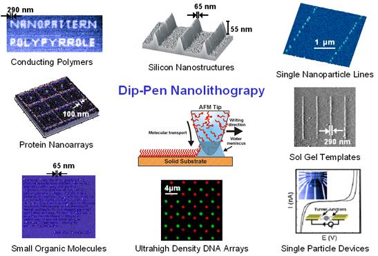
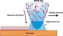
2 Top-Down Approach Mechanical energy Ball milling, polishing, grinding Thermal Annealing, evaporation, pyrolysis High energy Arch, laser, ion milling, reactive ion etching Chemical Chemical etching, CMP, electropolishing, anodizing Lithographic Photo, e-beam, EUV, X-ray, µ-cp, NIL, Nanosphere Nature Erosion, decomposition, digestion Bottom-Up Approach Gas Chemical vapor deposition, atomic layer deposition, MOCVD, MBE, ion implantation Liquid Self-assembly, supermolecule, reduction, template synthesis Lithographic Dip-pen, block co-polymer, STM writing Biological Protein, nuclear acidcrystal formation


3 Building a Computer ENIAC: Electronic Numerical Integrator And Computer, First Integrated Circuit "What we didn't realize then was that the integrated circuit would reduce the cost of electronic functions by a factor of a million to one, nothing had ever done that for anything before" - Jack Kilby 2000 Nobel Prize 1958 Texas Instruments

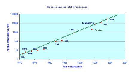
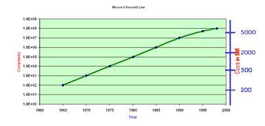
4 MOSFET Metal-Oxide-Semiconductor Field-Effect Transistor Small Print Low Power Dissipation Batch Process Fast Response Pure Electrical Switch, No Moving Parts Moore s Law


5 Tool Cost Why does the tool cost increase so fast? What is the bottleneck? Industrial Process Lithography Deposition Etching Planization Packaging
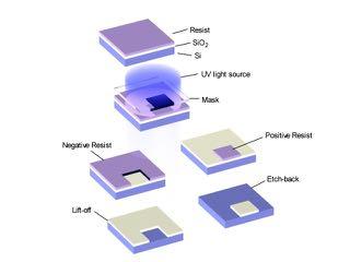

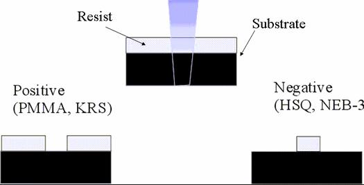
6 Photolithography Photoresist Positive tone Negative tone
-H 2 O 2 (30%) (Piranha Solution) 3:1 10-20 90 Oxide and Dissolve Organic and")
- H 2 O 2 (30%)-H 2 O 1:1:5 DI Water 5 Room T Spin Dry (In lad N 2 blow ) 10-20 90 Oxide and Dissolve Metals Washing STEP II: PR Spin")
7 STEP I: Cleaning RCA Cleaning (By Radio Corporation of America in 1965) Chemicals Volume ratio Procedure Time (min) Operation Temperature Function Trichlorothane 5 Room T Dissolve Organic Acetone 5 Room T Dissolve Organic DI Water 5 Room T Washing H 2 SO 4 (98%)-H 2 O 2 (30%) (Piranha Solution) 3: Oxide and Dissolve Organic and Metals DI Water 5 Room T Washing HF(49 wt %)-H 2 O 2: Room T Dissolve surface Si0 2 NH 4 OH(29%)-H 2 O 2 (30%)-H 2 O 1:1: Oxide and Dissolve Metals DI Water 5 Room T Washing HCl(37%)- H 2 O 2 (30%)-H 2 O 1:1:5 DI Water 5 Room T Spin Dry (In lad N 2 blow ) Oxide and Dissolve Metals Washing STEP II: PR Spin Coating/Soft Bake


8 Mask: Quartz + Cr Patterns STEP III: Align and Exposure STEP III: Align and Exposure UV light Off Align the pattern UV light On
 and")
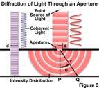
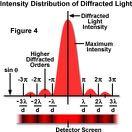
9 STEP IV: (PEB) and Develop Limitation of Optical Lithography r = 1.22 x λ/(2 x N.A.) N.A. = n x sin(θ)
 W min = k 1 λ/na")
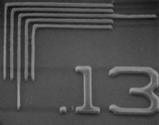
10 Diffraction Limit Resolution = K x λ/(n.a.) Depth of Focus = λ/(n.a.) 2 K = 0.61 Photolithogrpahy Types W min = k 1 sqrt(λd) W min = k 1 λ/na
 = K x λ/(n.a.) K = 0.")


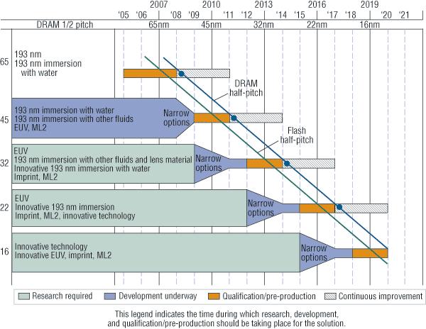
11 Photolithogrpahy Types Water Immersion Lithography Resolution (R) = K x λ/(n.a.) K = 0.25, NA ~1.4, λ = 193 R = 35 nm Air n= Water n = The resolution is increased by a factor equal to the refractive index of the liquid. Current immersion lithography tools use highly purified water for this liquid, achieving feature sizes below 45 nanometers.
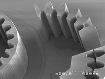
12 Trend of Lithography Nano/Micro Fabrication Lift-Off Etching


13 Thin Film Deposition Thermal Evaporator E-Beam Evaporator Sputter Etching (Wet and Dry) Wet Etching: Chemical Reactions Dry Etching: Physical (and Chemical) Reaction
 An ICP is different than an RIE")

, while the")

14 Reactive Ion Etching (RIE) Inductively Coupled Plasma (ICP) An ICP is different than an RIE because it uses two power supplies to generate plasma. One power source is used to generate a dense plasma (~10x more reactive species than RIE), while the second power source accelerates the ions towards the etching surface. This combination increases the anisotropy of the etched feature as compared to conventional RIE.


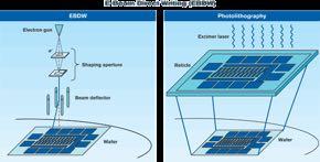
15 ICP and Bosch Process E-Beam Lithography
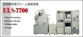
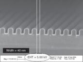
16 E-Beam Lithography E-Beam Lithography


17 Nanoimprint Lithography (NIL) Mold PMMA Substrate Imprint Remove Mold RIE Evaporation Lift-off (or Etching) Nanoimprint Lithography (NIL)


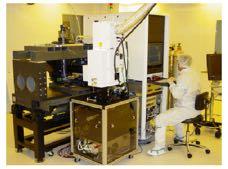
18 Step and Flash Imprint Lithography Nanoimprinter NX-2000, Nanoimprintor, Nanonex
 Lift-off")

")
")
19 Nanoimprint Results and Challenge Mask Fabrication (1:1) Lift-off process Resist Mask Design Soft Lithography Soft Lithography Microcontact Printing (µcp) Replica Molding (REM) Microtransfer Molding (µtm) Micromolding in Capillary (MIMIC) Solvent-Assisted Micromolding (SAMIM)

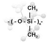
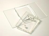
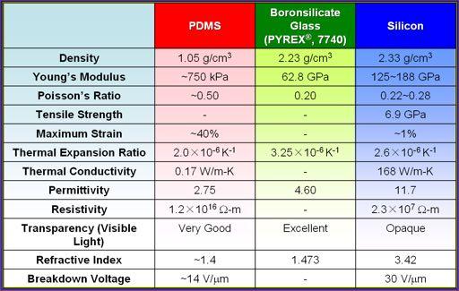
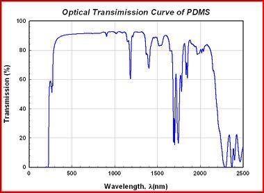
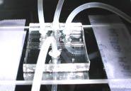
20 Soft Lithography - PDMS PDMS (Polydimethylsiloxane) PDMS is durable, optically transparent, and inexpensive PDMS can be patterned by Soft Lithography Silicone PDMS Microfluidic Channel PDMS Material Properties

 1 2")
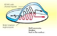
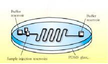
21 PDMS Replica Molding (REM) 1 2 Mold Patterning 3 PDMS Curing Bonding and Interconnecting


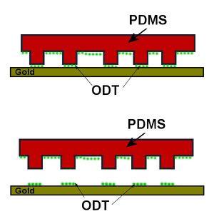
22 PDMS Curing and Bonding Curing of PDMS Bonding of PDMS Micro Contact Printing (µcp)


23 Others
EE40 Lec 22. IC Fabrication Technology. Prof. Nathan Cheung 11/19/2009
 Suggested Reading EE40 Lec 22 IC Fabrication Technology Prof. Nathan Cheung 11/19/2009 300mm Fab Tour http://www-03.ibm.com/technology/manufacturing/technology_tour_300mm_foundry.html Overview of IC Technology
Fabrication Technology
 Fabrication Technology By B.G.Balagangadhar Department of Electronics and Communication Ghousia College of Engineering, Ramanagaram 1 OUTLINE Introduction Why Silicon The purity of Silicon Czochralski
VLSI Technology. By: Ajay Kumar Gautam
 By: Ajay Kumar Gautam Introduction to VLSI Technology, Crystal Growth, Oxidation, Epitaxial Process, Diffusion Process, Ion Implantation, Lithography, Etching, Metallization, VLSI Process Integration,
Ajay Kumar Gautam [VLSI TECHNOLOGY] VLSI Technology for 3RD Year ECE/EEE Uttarakhand Technical University
![Ajay Kumar Gautam [VLSI TECHNOLOGY] VLSI Technology for 3RD Year ECE/EEE Uttarakhand Technical University](/thumbs/75/72824557.jpg "Ajay Kumar Gautam [VLSI TECHNOLOGY] VLSI Technology for 3RD Year ECE/EEE Uttarakhand Technical University") 2014 Ajay Kumar Gautam [VLSI TECHNOLOGY] VLSI Technology for 3RD Year ECE/EEE Uttarakhand Technical University Page1 Syllabus UNIT 1 Introduction to VLSI Technology: Classification of ICs, Scale of integration,
2014 Ajay Kumar Gautam [VLSI TECHNOLOGY] VLSI Technology for 3RD Year ECE/EEE Uttarakhand Technical University Page1 Syllabus UNIT 1 Introduction to VLSI Technology: Classification of ICs, Scale of integration,
Nanofabrication Prof. Stephen Y. Chou NanoStructure Laboratory
 Nanofabrication Prof. Stephen Y. Chou Department of Electrical Engineering Princeton University 1 Acknowledgment Dr. Paul Fischer Dr. Yun Wang Dr. Jay Guo Dr. Peter Klauss Dr. Jim Wang Dr. Longtin He Dr.
Photoresist Coat, Expose and Develop Laboratory Dr. Lynn Fuller
 ROCHESTER INSTITUTE OF TECHNOLOGY MICROELECTRONIC ENGINEERING Photoresist Coat, Expose and Develop Laboratory Dr. Lynn Fuller Webpage: http://www.rit.edu/lffeee 82 Lomb Memorial Drive Rochester, NY 14623-5604
Fabrication Techniques for Thin-Film Silicon Layer Transfer
 Fabrication Techniques for Thin-Film Silicon Layer Transfer S. L. Holl a, C. A. Colinge b, S. Song b, R. Varasala b, K. Hobart c, F. Kub c a Department of Mechanical Engineering, b Department of Electrical
Technology. Semiconductor Manufacturing. Hong Xiao INTRODUCTION TO SECOND EDITION SPIE PRESS
 INTRODUCTION TO Semiconductor Manufacturing Technology SECOND EDITION Hong Xiao TECHNISCHE INFORMATIONSBiBUOTHEK UNIVERSITATSBIBLIOTHEK HANNOVER SPIE PRESS Bellingham,Washington USA Contents Preface to
KGC SCIENTIFIC Making of a Chip
 KGC SCIENTIFIC www.kgcscientific.com Making of a Chip FROM THE SAND TO THE PACKAGE, A DIAGRAM TO UNDERSTAND HOW CPU IS MADE? Sand CPU CHAIN ANALYSIS OF SEMICONDUCTOR Material for manufacturing process
In-Situ Monitoring of Pattern Filling in Nano-Imprint Lithography Using Surface Plasmon Resonance
 Copyright 2011 American Scientific Publishers All rights reserved Printed in the United States of America Journal of Nanoscience and Nanotechnology Vol. 11, 1 6, 2011 In-Situ Monitoring of Pattern Filling
Micro-Electro-Mechanical Systems (MEMS) Fabrication. Special Process Modules for MEMS. Principle of Sensing and Actuation
 Fabrication. Special Process Modules for MEMS. Principle of Sensing and Actuation") Micro-Electro-Mechanical Systems (MEMS) Fabrication Fabrication Considerations Stress-Strain, Thin-film Stress, Stiction Special Process Modules for MEMS Bonding, Cavity Sealing, Deep RIE, Spatial forming
Micro-Electro-Mechanical Systems (MEMS) Fabrication Fabrication Considerations Stress-Strain, Thin-film Stress, Stiction Special Process Modules for MEMS Bonding, Cavity Sealing, Deep RIE, Spatial forming
Surface micromachining and Process flow part 1
 Surface micromachining and Process flow part 1 Identify the basic steps of a generic surface micromachining process Identify the critical requirements needed to create a MEMS using surface micromachining
Lab #2 Wafer Cleaning (RCA cleaning)
") Lab #2 Wafer Cleaning (RCA cleaning) RCA Cleaning System Used: Wet Bench 1, Bay1, Nanofabrication Center Chemicals Used: H 2 O : NH 4 OH : H 2 O 2 (5 : 1 : 1) H 2 O : HF (10 : 1) H 2 O : HCl : H 2 O 2
Lab #2 Wafer Cleaning (RCA cleaning) RCA Cleaning System Used: Wet Bench 1, Bay1, Nanofabrication Center Chemicals Used: H 2 O : NH 4 OH : H 2 O 2 (5 : 1 : 1) H 2 O : HF (10 : 1) H 2 O : HCl : H 2 O 2
Lecture 19 Microfabrication 4/1/03 Prof. Andy Neureuther
 EECS 40 Spring 2003 Lecture 19 Microfabrication 4/1/03 Prof. ndy Neureuther How are Integrated Circuits made? Silicon wafers Oxide formation by growth or deposition Other films Pattern transfer by lithography
Integration of Block-Copolymer with Nano- Imprint Lithography: Pushing the Boundaries of Emerging Nano-Patterning Technology
 Integration of Block-Copolymer with Nano- Imprint Lithography: Pushing the Boundaries of Emerging Nano-Patterning Technology April 2010 update SNL Geoff Brennecka (PI) Bruce Burckel Matt George Jack Skinner
Atomic Layer Deposition(ALD)
") Atomic Layer Deposition(ALD) AlO x for diffusion barriers OLED displays http://en.wikipedia.org/wiki/atomic_layer_deposition#/media/file:ald_schematics.jpg Lam s market-leading ALTUS systems combine CVD
Atomic Layer Deposition(ALD) AlO x for diffusion barriers OLED displays http://en.wikipedia.org/wiki/atomic_layer_deposition#/media/file:ald_schematics.jpg Lam s market-leading ALTUS systems combine CVD
micro resist technology
 Characteristics Processing guidelines Negative Tone Photoresist Series ma-n 2400 ma-n 2400 is a negative tone photoresist series designed for the use in micro- and nanoelectronics. The resists are available
Processing guidelines
 Processing guidelines mr-uvcur21 series UV-curable Polymer for UV-based Nanoimprint Lithography Characteristics mr-uvcur21 is a liquid UV-curable polymer system with low viscosity and high curing rate
Silicon Wafer Processing PAKAGING AND TEST
 Silicon Wafer Processing PAKAGING AND TEST Parametrical test using test structures regularly distributed in the wafer Wafer die test marking defective dies dies separation die fixing (not marked as defective)
Process Flow in Cross Sections
 Process Flow in Cross Sections Process (simplified) 0. Clean wafer in nasty acids (HF, HNO 3, H 2 SO 4,...) --> wear gloves! 1. Grow 500 nm of SiO 2 (by putting the wafer in a furnace with O 2 2. Coat
Processing guidelines. Negative Tone Photoresist Series ma-n 2400
 Characteristics Processing guidelines Negative Tone Photoresist Series ma-n 2400 ma-n 2400 is a negative tone photoresist series designed for the use in micro- and nanoelectronics. The resists are available
Vertically aligned Ni magnetic nanowires fabricated by diblock-copolymer-directed Al thin film anodization
 Vertically aligned Ni magnetic nanowires fabricated by diblock-copolymer-directed Al thin film anodization Researcher: Kunbae (Kevin) Noh, Graduate Student, MAE Dept. and CMRR Collaborators: Leon Chen,
Supporting Information
 Supporting Information Fast-Response, Sensitivitive and Low-Powered Chemosensors by Fusing Nanostructured Porous Thin Film and IDEs-Microheater Chip Zhengfei Dai,, Lei Xu,#,, Guotao Duan *,, Tie Li *,,
Gaetano L Episcopo. Introduction to MEMS
 Gaetano L Episcopo Introduction to MEMS What are MEMS? Micro Electro Mechanichal Systems MEMS are integrated devices, or systems of devices, with microscopic parts, such as: Mechanical Parts Electrical
BASICS OF MANUFACTURING INTEGRATED CIRCUITS
 BASICS OF MANUFACTURING INTEGRATED CIRCUITS Opportunities for filtration exist for the manufacture of very small electronic components referred to as semiconductors. This broad category includes devices
Lecture 10: MultiUser MEMS Process (MUMPS)
") MEMS: Fabrication Lecture 10: MultiUser MEMS Process (MUMPS) Prasanna S. Gandhi Assistant Professor, Department of Mechanical Engineering, Indian Institute of Technology, Bombay, 1 Recap Various VLSI based
MEMS: Fabrication Lecture 10: MultiUser MEMS Process (MUMPS) Prasanna S. Gandhi Assistant Professor, Department of Mechanical Engineering, Indian Institute of Technology, Bombay, 1 Recap Various VLSI based
Photolithography I ( Part 2 )
") 1 Photolithography I ( Part 2 ) Chapter 13 : Semiconductor Manufacturing Technology by M. Quirk & J. Serda Bjørn-Ove Fimland, Department of Electronics and Telecommunication, Norwegian University of Science
1 Photolithography I ( Part 2 ) Chapter 13 : Semiconductor Manufacturing Technology by M. Quirk & J. Serda Bjørn-Ove Fimland, Department of Electronics and Telecommunication, Norwegian University of Science
Positive Photoresists
 Positive Photoresists Gesellschaft für chemische Materialien spezieller Photoresistsysteme mbh Positive Photoresists map 1200 series Thick resists map 1275, map 1275 HV Unique features of the positive
Report 1. B. Starting Wafer Specs Number: 10 Total, 6 Device and 4 Test wafers
 Aaron Pederson EE 432 Lab Dr. Meng Lu netid: abp250 Lab instructor: Yunfei Zhao Report 1 A. Overview The goal of this lab is to go through the semiconductor fabrication process from start to finish. This
Introduction to MEMS
 Introduction to MEMS 520.487 Lecture Outline 1. Photolithography 2. Thermal Oxidation 3. Wet Etching 4. Dry Etching 5. Unconventional Microfabrication Photolithography Conventional Photoresists Typically
ME 141B: The MEMS Class Introduction to MEMS and MEMS Design. Sumita Pennathur UCSB
 ME 141B: The MEMS Class Introduction to MEMS and MEMS Design Sumita Pennathur UCSB Outline Class odds and ends Intro to Your Device Process Flow for Your Device Microfabrication Outline Suggested groups
How To Write A Flowchart
 1 Learning Objectives To learn how you transfer a device concept into a process flow to fabricate the device in the EKL labs You learn the different components that makes up a flowchart; process blocks,
Metallization deposition and etching. Material mainly taken from Campbell, UCCS
 Metallization deposition and etching Material mainly taken from Campbell, UCCS Application Metallization is back-end processing Metals used are aluminum and copper Mainly involves deposition and etching,
Delamination of Thin Films Using Laser Induced Stress Waves
 Center for Nanoscale Chemical-Electrical-Mechanical Manufacturing Systems Delamination of Thin Films Using Laser Induced Stress Waves Undergraduate Researcher Angelica Anne Vargas, Research Experience
PROCESSING OF INTEGRATED CIRCUITS
 PROCESSING OF INTEGRATED CIRCUITS Overview of IC Processing (Part I) Silicon Processing Lithography Layer Processes Use in IC Fabrication (Part II) Integrating the Fabrication Steps IC Packaging (Part
3.155J / 6.152J Micro/Nano Processing Technology TAKE-HOME QUIZ FALL TERM 2005
 3.155J / 6.152J Micro/Nano Processing Technology TAKE-HOME QUIZ FALL TERM 2005 1) This is an open book, take-home quiz. You are not to consult with other class members or anyone else. You may discuss the
5.8 Diaphragm Uniaxial Optical Accelerometer
 5.8 Diaphragm Uniaxial Optical Accelerometer Optical accelerometers are based on the BESOI (Bond and Etch back Silicon On Insulator) wafers, supplied by Shin-Etsu with (100) orientation, 4 diameter and
EE C245 ME C218 Introduction to MEMS Design Fall 2011
 Lecture Outline EE C245 ME C218 Introduction to MEMS Design Fall 2011 Prof. Clark T.-C. Nguyen Dept. of Electrical Engineering & Computer Sciences University of California at Berkeley Berkeley, CA 94720
Uncrosslinked SU-8 as a sacrificial material
 INSTITUTE OFPHYSICS PUBLISHING JOURNAL OF MICROMECHANICS AND MICROENGINEERING J. Micromech. Microeng. 15 (2005) N1 N5 doi:10.1088/0960-1317/15/1/n01 TECHNICAL NOTE Uncrosslinked as a sacrificial material
Process steps for Field Emitter devices built on Silicon wafers And 3D Photovoltaics on Silicon wafers
 Process steps for Field Emitter devices built on Silicon wafers And 3D Photovoltaics on Silicon wafers David W. Stollberg, Ph.D., P.E. Research Engineer and Adjunct Faculty GTRI_B-1 Field Emitters GTRI_B-2
Micropatterning and casting PEDOT-PSS /DMSO layers
 Micropatterning and casting PEDOT-PSS /DMSO layers Benoît Charlot, Gilbert Sassine, Alexandra Garraud, Alain Giani, Philippe Combette IES Institut d Electronique du Sud CNRS Université Montpellier II Place&E.&Bataillon,&34095&Montpellier&7&France&
Ultra High Barrier Coatings by PECVD
 Society of Vacuum Coaters 2014 Technical Conference Presentation Ultra High Barrier Coatings by PECVD John Madocks & Phong Ngo, General Plasma Inc., 546 E. 25 th Street, Tucson, Arizona, USA Abstract Silicon
Copyright. Stephen Christopher Johnson
 Copyright by Stephen Christopher Johnson 2005 The Dissertation Committee for Stephen Christopher Johnson Certifies that this is the approved version of the following dissertation: Step and Flash Imprint
Semiconductor Manufacturing Technology. IC Fabrication Process Overview
 Semiconductor Manufacturing Technology Michael Quirk & Julian Serda October 00 by Prentice Hall Chapter 9 IC Fabrication Process Overview /4 Objectives After studying the material in this chapter, you
From microelectronics down to nanotechnology.
 From microelectronics down to nanotechnology sami.franssila@tkk.fi Contents Lithography: scaling x- and y-dimensions MOS transistor physics Scaling oxide thickness (z-dimension) CNT transistors Conducting
MCC. PMGI Resists NANO PMGI RESISTS OFFER RANGE OF PRODUCTS
 MCC PMGI RESISTS OFFER Sub.25µm lift-off processing Film thicknesses from 5µm Choice of resin blends for optimal undercut control High thermal stability Superior adhesion to Si, NiFe, GaAs, InP
Oxide Growth. 1. Introduction
 Oxide Growth 1. Introduction Development of high-quality silicon dioxide (SiO2) has helped to establish the dominance of silicon in the production of commercial integrated circuits. Among all the various
Surface Micromachining
 Surface Micromachining Outline Introduction Material often used in surface micromachining Material selection criteria in surface micromachining Case study: Fabrication of electrostatic motor Major issues
Lecture 6. Through-Wafer Interconnect. Agenda: Through-wafer Interconnect Polymer MEMS. Through-Wafer Interconnect -1. Through-Wafer Interconnect -2
 Agenda: EEL6935 Advanced MEMS (Spring 2005) Instructor: Dr. Huikai Xie Lecture 6 Through-wafer Interconnect EEL6935 Advanced MEMS 2005 H. Xie 1/21/2005 1 Motivations: Wafer-level packaging CMOS 3D Integration
CHAPTER 1 HOW SEMICONDUCTOR CHIPS ARE MADE
 CHAPTER 1 HOW SEMICONDUCTOR CHIPS ARE MADE Hwaiyu Geng Hewlett-Packard Company Palo Alto, California Lin Zhou Intel Corporation Hillsboro, Oregon 1.1 INTRODUCTION Over the past decades, an information
Regents of the University of California
 Surface-Micromachining Process Flow Photoresist Sacrificial Oxide Structural Polysilcon Deposit sacrificial PSG: Target = 2 m 1 hr. 40 min. LPCVD @450 o C Densify the PSG Anneal @950 o C for 30 min. Lithography
LANDOLT-BÖRNSTEIN. Zahlenwerte und Funktionen aus Naturwissenschaften und Technik. Neue Serie. Gesamtherausgabe: K.-H. Hellwege O.
 LANDOLT-BÖRNSTEIN Zahlenwerte und Funktionen aus Naturwissenschaften und Technik Neue Serie Gesamtherausgabe: K.-H. Hellwege O. Madelung Gruppe III: Kristall- und Festkörperphysik Band 17 Halbleiter Herausgeber:
Step and Flash Imprint Lithography for sub-100nm Patterning
 Step and Flash Imprint Lithography for sub-100nm Patterning Matthew Colburn, Annette Grot, Marie Amistoso, Byung Jin Choi, Todd Bailey, John Ekerdt, S.V. Sreenivasan, James Hollenhorst, C. Grant Willson
Alternative Methods of Yttria Deposition For Semiconductor Applications. Rajan Bamola Paul Robinson
 Alternative Methods of Yttria Deposition For Semiconductor Applications Rajan Bamola Paul Robinson Origin of Productivity Losses in Etch Process Aggressive corrosive/erosive plasma used for etch Corrosion/erosion
Superionic Solid State Stamping (S4)
") Superionic Solid State Stamping (S4) Lead Faculty Researcher: Placid Ferreira Department: Materials Science & Engineering Hsu et al, Nano Letters, 2007 1. Description: This dry, single step, electrochemical
Superionic Solid State Stamping (S4) Lead Faculty Researcher: Placid Ferreira Department: Materials Science & Engineering Hsu et al, Nano Letters, 2007 1. Description: This dry, single step, electrochemical
Multiphoton lithography based 3D micro/nano printing Dr Qin Hu
 Multiphoton lithography based 3D micro/nano printing Dr Qin Hu EPSRC Centre for Innovative Manufacturing in Additive Manufacturing University of Nottingham Multiphoton lithography Also known as direct
Cristina Rusu Imego AB Cristina Rusu
 MEMS Fabrication Cristina Rusu Imego AB 2011-02-21 MEMS Semiconductors as mechanical materials Bulk micromachining Dry etching Wet etching Surface micromachining MUMPs Polymer MEMS Wafer bonding Technology:
INTERVIA BPP-10 Photoresist
 Technical Data Sheet INTERVIA BPP-10 Photoresist For Advanced Packaging Applications Description Regional Product Availability Advantages INTERVIA BPP-10 Photoresist is a general-purpose, multi-wavelength
ME 189 Microsystems Design and Manufacture. Chapter 9. Micromanufacturing
 ME 189 Microsystems Design and Manufacture Chapter 9 Micromanufacturing This chapter will offer an overview of the application of the various fabrication techniques described in Chapter 8 in the manufacturing
Figure 2.3 (cont., p. 60) (e) Block diagram of Pentium 4 processor with 42 million transistors (2000). [Courtesy Intel Corporation.
 (e) Block diagram of Pentium 4 processor with 42 million transistors (2000). [Courtesy Intel Corporation.") Figure 2.1 (p. 58) Basic fabrication steps in the silicon planar process: (a) oxide formation, (b) selective oxide removal, (c) deposition of dopant atoms on wafer, (d) diffusion of dopant atoms into exposed
Figure 2.1 (p. 58) Basic fabrication steps in the silicon planar process: (a) oxide formation, (b) selective oxide removal, (c) deposition of dopant atoms on wafer, (d) diffusion of dopant atoms into exposed
Sub-5 nm Structures Process Development and Fabrication Over Large Areas
 A S Jugessur,, 2017, 1:1 SciFed Nanotech Research Letters Research Article Open Access Sub-5 nm Structures Process Development and Fabrication Over Large Areas * A S Jugessur * University of Iowa Microfabrication
Lecture 5. SOI Micromachining. SOI MUMPs. SOI Micromachining. Silicon-on-Insulator Microstructures. Agenda:
 EEL6935 Advanced MEMS (Spring 2005) Instructor: Dr. Huikai Xie SOI Micromachining Agenda: SOI Micromachining SOI MUMPs Multi-level structures Lecture 5 Silicon-on-Insulator Microstructures Single-crystal
Deep Lithography for Microfabrication
 Deep Lithography for Microfabrication Part 2: UV Deep Lithography (UVDL) Luiz O. S. Ferreira Mechanical Engineering Faculty Campinas State University UNICAMP Campinas SP - BRAZIL lotavio@fem.unicamp.br
EXPLORING VACUUM CASTING TECHNIQUES FOR MICRON AND SUBMICRON FEATURES. Campus Ker Lann, av Robert Schumann Bruz, France
 EXPLORING VACUUM CASTING TECHNIQUES FOR MICRON AND SUBMICRON FEATURES M. Denoual *, P. Mognol **, B. Lepioufle * * Biomis-SATIE ENS-Cachan antenne de Bretagne, Campus Ker Lann, av Robert Schumann 35170
UV5 POSITIVE DUV PHOTORESIST For Microlithography Applications
 UV5 POSITIVE DUV PHOTORESIST For Microlithography Applications DESCRIPTION UV5 positive DUV photoresist has been optimized to provide vertical profile imaging of isolated and semidense features for device
Electron Microscopy Sciences Industry Road. P.O. Box 550. Hatfield, PA Introduction. DuraSiNTM
 DuraSiNTM Electron Microscopy Sciences Introduction DuraSiN TM Film and Mesh products have revolutionized the way samples are prepared for and analyzed in the transmission electron microscope. DuraSiN
Leveraging the Precision of Electroforming over Alternative Processes When Developing Nano-scale Structures
 VOLUME 4 - ELECTROFORMING Leveraging the Precision of over Alternative Processes When Developing Nano-scale Structures Electrical and mechanical component and subsystem designers generally have five techniques
SU Permanent Epoxy Negative Photoresist PROCESSING GUIDELINES FOR:
 SU-8 2000 Permanent Epoxy Negative Photoresist PROCESSING GUIDELINES FOR: SU-8 2100 and SU-8 2150 www.microchem.com SU-8 2000 is a high contrast, epoxy based photoresist designed for micromachining and
CMOS Manufacturing process. Circuit designer. Design rule set. Process engineer. Set of optical masks. Fabrication process.
 CMOS Manufacturing process Circuit design Set of optical masks Fabrication process Circuit designer Design rule set Process engineer All material: Chap. 2 of J. Rabaey, A. Chandrakasan, B. Nikolic, Digital
Radiation Tolerant Isolation Technology
 Radiation Tolerant Isolation Technology Background The following contains a brief description of isolation technologies used for radiation hardened integrated circuits. The technologies mentioned are junction
1. Introduction. What is implantation? Advantages
 Ion implantation Contents 1. Introduction 2. Ion range 3. implantation profiles 4. ion channeling 5. ion implantation-induced damage 6. annealing behavior of the damage 7. process consideration 8. comparison
Plasma..TI'1eITI1 I.P.
 Plasma..TI'1eITI1 I.P. RPPI..ICRTION NOTES PLASMA ETCHING OF SIUCON NITRIDE AND SIUCON DIOXIDE Silicon nitride and silicon dioxide thin films find e variety of uses in both semiconductor and nonsemiconductor
Advanced developer-soluble gap-fill materials and applications
 Advanced developer-soluble gap-fill materials and applications Runhui Huang, Dan Sullivan, Anwei Qin, Shannon Brown Brewer Science, Inc., 2401 Brewer Dr., Rolla, MO, USA, 65401 ABSTRACT For the via-first
A Quick Overview of Micromachining for MEMS Designers
 A Quick Overview of Micromachining for MEMS Designers A designer has control over two sets of variables: materials and the shapes of parts. M. F. Ashby Manufacturing determines which materials can be processed
Presented at the 28th European PV Solar Energy Conference and Exhibition, 30 September 4 October, 2013, Paris, France
 INTEGRATING DIFFRACTIVE REAR SIDE STRUCTURES FOR LIGHT TRAPPING INTO CRYSTALLINE SILICON SOLAR CELLS J. Eisenlohr 1*, H. Hauser 1, J. Benick 1, A. Mellor 2, B. Bläsi 1, J.C. Goldschmidt 1, M. Hermle 1
CMOS FABRICATION. n WELL PROCESS
 CMOS FABRICATION n WELL PROCESS Step 1: Si Substrate Start with p- type substrate p substrate Step 2: Oxidation Exposing to high-purity oxygen and hydrogen at approx. 1000 o C in oxidation furnace SiO
Novel Solutions for ESD Sensitive Devices
 Novel Solutions for ESD Sensitive Devices Chris Schreiber Magnecomp cschreiber@magnecomp.com Safely Dissipating ESD Problem Static Charging is created by either Tribocharging or Induction and the uncontrolled
High-Resolution, Electrohydrodynamic Inkjet Printing of Stretchable, Metal Oxide Semiconductor Transistors with High Performances
 Electronic Supplementary Material (ESI) for Nanoscale. This journal is The Royal Society of Chemistry 2016 ` Electronic Supplementary Information High-Resolution, Electrohydrodynamic Inkjet Printing of
2. High Efficiency Crystalline Si Solar Cells
 2 High Efficiency Crystalline Si Solar Cells Students: Karthick Murukesan, Sandeep S S, Meenakshi Bhaisare, Bandana Singha, Kalaivani S and Ketan Warikoo Faculty members: Anil Kottantharayil, B M Arora,
Mold Fabrication for 3D Dual Damascene Imprinting
 Nanoscale Res Lett (2010) 5:545 549 DOI 10.1007/s11671-010-9540-2 SPECIAL ISSUE ARTICLE Mold Fabrication for 3D Dual Damascene Imprinting S. M. Saydur Rahman Bo Cui Received: 11 September 2009 / Accepted:
LOT. Contents. Introduction to Thin Film Technology. Chair of Surface and Materials Technology
 Introduction to Thin Film Contents 1. Introduction and Application Examples (2h) 2. Preparation of Thin Films by PVD (Physical Vapor Deposition) (6h) 2.1 Vacuum Technique (1h) 2.1.1 Kinetics of Gases 2.1.2
Innovation Creativity customer-specific solutions. Product information PHOTORESISTS
 Product information PHOTORESISTS 1 Customer-specific solutions THE ALLRESIST GMBH Company for chemical Products OUR NEWS for Microstructuring As of January 2016 The executive board The company is represented
Optical characterization of an amorphoushydrogenated carbon film and its application in phase modulated diffractive optical elements
 Optical characterization of an amorphoushydrogenated carbon film and its application in phase modulated diffractive optical elements G. A. Cirino a, P. Verdonck a, R. D. Mansano a, L. G. Neto b a LSI-PEE-EPUSP
Technical Data Sheet Technisches Datenblatt
 AZ ECI 3000 Photoresist Universal i-line/crossover Photoresist Series GENERAL INFORMATION AZ ECI 3000 photoresist series are a family of fast positive resists with high resolution capabilities (0.4 µm
State of the art quality of a GeOx interfacial passivation layer formed on Ge(001)
") APPLICATION NOTE State of the art quality of a Ox interfacial passivation layer formed on (001) Summary A number of research efforts have been made to realize Metal-Oxide-Semiconductor Field Effect Transistors
APPLICATION NOTE State of the art quality of a Ox interfacial passivation layer formed on (001) Summary A number of research efforts have been made to realize Metal-Oxide-Semiconductor Field Effect Transistors
Soft-lithography for Preparing Patterned Liquid Crystal Orientations
 2007 KIDS Soft-lithography for Preparing Patterned Liquid Crystal Orientations Hak-Rin Kim **a, Jong-Wook Jung **a, Min-Soo Shin **a, Myung-Eun Kim a, You-Jin Lee **a, and Jae-Hoon Kim *b Abstract We demonstrate
A Deep Silicon RIE Primer Bosch Etching of Deep Structures in Silicon
 A Deep Silicon RIE Primer Bosch Etching of Deep Structures in Silicon April 2009 A Deep Silicon RIE Primer 1.0) Etching: Silicon does not naturally etch anisotropically in fluorine based chemistries. Si
3D technologies for integration of MEMS
 3D technologies for integration of MEMS, Fraunhofer Institute for Electronic Nano Systems Folie 1 Outlook Introduction 3D Processes Process integration Characterization Sample Applications Conclusion Folie
Plasma for Underfill Process in Flip Chip Packaging
 Plasma for Underfill Process in Flip Chip Packaging Jack Zhao and James D. Getty Nordson MARCH 2470-A Bates Avenue Concord, California 94520-1294 USA Published by Nordson MARCH www.nordsonmarch.com 2015
Today s agenda (19-JAN-2010)
") Today s agenda (19-JAN-2010) 1) Overview of Integrated Circuit technology 2) Managing Deadlines 3) A look @ Spring Schedule 4) Suggested milestones 5) Project concept presentations Action items from last
Today s agenda (19-JAN-2010) 1) Overview of Integrated Circuit technology 2) Managing Deadlines 3) A look @ Spring Schedule 4) Suggested milestones 5) Project concept presentations Action items from last
Lecture 4. Oxidation (applies to Si and SiC only) Reading: Chapter 4
 Reading: Chapter 4") Lecture 4 Oxidation (applies to Si and SiC only) Reading: Chapter 4 Introduction discussion: Oxidation: Si (and SiC) Only The ability to grow a high quality thermal oxide has propelled Si into the forefront
Lecture 4 Oxidation (applies to Si and SiC only) Reading: Chapter 4 Introduction discussion: Oxidation: Si (and SiC) Only The ability to grow a high quality thermal oxide has propelled Si into the forefront
PARAMETER EFFECTS FOR THE GROWTH OF THIN POROUS ANODIC ALUMINUM OXIDES
 10.1149/1.2794473, The Electrochemical Society PARAMETER EFFECTS FOR THE GROWTH OF THIN POROUS ANODIC ALUMINUM OXIDES S. Yim a, C. Bonhôte b, J. Lille b, and T. Wu b a Dept. of Chem. and Mat. Engr., San
CMOS Manufacturing Process
 CMOS Manufacturing Process CMOS Process A Modern CMOS Process gate-oxide TiSi 2 AlCu Tungsten SiO 2 n+ p-well p-epi poly n-well p+ SiO 2 p+ Dual-Well Trench-Isolated CMOS Process Circuit Under Design V
Procese de depunere in sistemul Plasma Enhanced Chemical Vapor Deposition (PECVD)
") Procese de depunere in sistemul Plasma Enhanced Chemical Vapor Deposition (PECVD) Ciprian Iliescu Conţinutul acestui material nu reprezintă in mod obligatoriu poziţia oficială a Uniunii Europene sau a
Procese de depunere in sistemul Plasma Enhanced Chemical Vapor Deposition (PECVD) Ciprian Iliescu Conţinutul acestui material nu reprezintă in mod obligatoriu poziţia oficială a Uniunii Europene sau a
Plasma Etching Rates & Gases Gas ratios affects etch rate & etch ratios to resist/substrate
 Plasma Etching Rates & Gases Gas ratios affects etch rate & etch ratios to resist/substrate Development of Sidewalls Passivating Films Sidewalls get inert species deposited on them with plasma etch Creates
Specimen Preparation Technique for a Microstructure Analysis Using the Focused Ion Beam Process
 Specimen Preparation Technique for a Microstructure Analysis Using the Focused Ion Beam Process by Kozue Yabusaki * and Hirokazu Sasaki * In recent years the FIB technique has been widely used for specimen
EXCIMER LASER ANNEALING FOR LOW- TEMPERATURE POLYSILICON THIN FILM TRANSISTOR FABRICATION ON PLASTIC SUBSTRATES
 EXCIMER LASER ANNEALING FOR LOW- TEMPERATURE POLYSILICON THIN FILM TRANSISTOR FABRICATION ON PLASTIC SUBSTRATES G. Fortunato, A. Pecora, L. Maiolo, M. Cuscunà, D. Simeone, A. Minotti, and L. Mariucci CNR-IMM,
St.JOHNS COLLEGE OF ENGINEERING AND TECHNOLOGY,
 PRESENTED BY S.SRIKANTH REDDY Y.MARUTHI III B.tech III.B.tech Sri.prince087@gmail.com St.JOHNS COLLEGE OF ENGINEERING AND TECHNOLOGY, YERRAKOTA, YEMIGANUR, KURNOOL (Dist), ANDHRA PRADESH. ABSTRACT VLSI
Ultra Fine Pitch Bumping Using e-ni/au and Sn Lift-Off Processes
 Ultra Fine Pitch Bumping Using e-ni/au and Sn Lift-Off Processes Andrew Strandjord, Thorsten Teutsch, and Jing Li Pac Tech USA Packaging Technologies, Inc. Santa Clara, CA USA 95050 Thomas Oppert, and
Amorphous Oxide Transistor Electrokinetic Reflective Display on Flexible Glass
 Amorphous Oxide Transistor Electrokinetic Reflective Display on Flexible Glass Devin A. Mourey, Randy L. Hoffman, Sean M. Garner *, Arliena Holm, Brad Benson, Gregg Combs, James E. Abbott, Xinghua Li*,