Dicing Glass Optical Devices
|
|
|
- Evan Warner
- 6 years ago
- Views:
Transcription
1
2 Glass Applications


3 Dicing Glass Optical Devices -Blade Characteristics 2,, 4 4 Resin Type Q Diamond grit size: mic. Thickness: (0.15mm 0.3mm) Metal Sintered E08 & New matrices mic. Thickness Cutting Parameters Feed rate: mm/sec Spindle speed: 2 : : krpm 4 : : krpm
4 Dicing Glass & Fiber Optic Applications Dicing Glass Characteristics: Brittle material tends to chip Relatively soft material Will load during dicing - Cut perpendicularity problems Problematic mounting - Back side chipping Surface finish issues
5 Dicing Glass & Fiber Optic Applications Diamond Material Knoop Hardness Sapphire Alumina Titanium Carbide TiC Silicon High speed steel Quartz Glass [BK7][560] Barium Fluoride
6 Dicing Glass & Fiber Optic Applications Nickel Binders Will Overload Metal * Sintered May Work only On some thin Substrates Resinoid Binders * Perform with Minimum loading And best cut quality * Nickel & M. Sintered Matrices can be used on some special Glass applications
7 Dicing Glass & Fiber Optic Applications Self resharpening blade Resin wearing out High Temperatures Resin Diamond Blade wear

8 Dicing Glass & Fiber Optic Applications Resinoid - matrix characteristics Resin No nickel coating on Diamonds. Diamond Two stage curing. Carbon powder for electrical conductivity. * Higher wear. * Finer cut.


9 Dicing Glass & Fiber Optic Applications Resinoid - Low diamond % * Less loading. * Freer dicing. * Higher wear. * Better cut quality. Powder residue.

10 Dicing Glass & Fiber Optic Applications Resinoid - wear mechanism: Diamond gets loose due to vibration movements in the resin binder Forces on the diamonds during the dicing process Diamond wearing out
11 Dicing Glass & Fiber Optic Applications Popular resin binders for dicing glass QUP QKP QIP Harder Softer P/N Example QUP Diamond grit sizes: mic. 3 & 6mic. For special communication app.
12 Thick glass substrates: Dicing Glass & Fiber Optic Applications Glass 8-12mm -SPG + Larger Diamond grits Up to 88mic. Minimizes loads and wear during the dicing process Min. thickness.015, in some cases.012 Can be used with standard flange sets or with high cooling flange sets
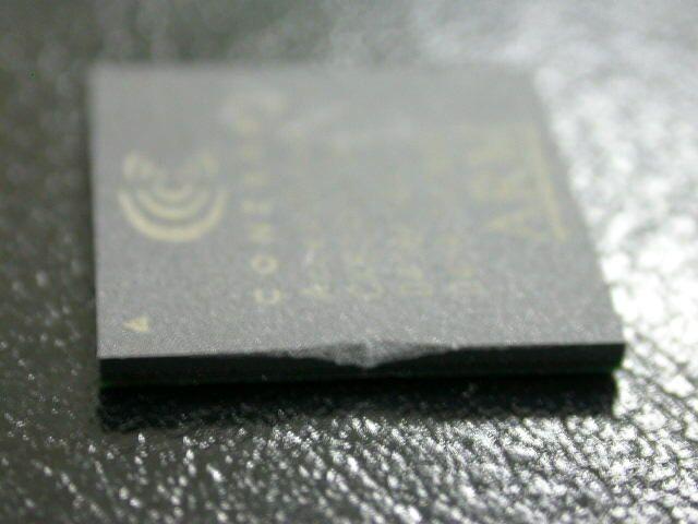
13 Dicing Glass & Fiber Optic Applications Application Test - # 1 Substrate: Material: Glass - Sio2 Substrate size: - 1 x 1 Thickness: - 0.2mm [.0078 ] Cutting parameters: Spindle:- 26Krpm Feed rate:- 1mm/sec Cut depth:-.010 [0.25mm/sec] Coolant:- Tap water 3.5 L / min. Saw being used: - ADT / 2 Process: Mounting:- UV Advill D-210 Blade matrix:- ADT Resinoid Blade O.D.: Blade thickness:-.006 [.152mm] Blade exposure:-.033 [0.86mm] Diamond grit:- 20mic. Blade P/N: QIP Cutting results: Top side chipping - < [ 0.020mm] Cracks - No Cracks Final Die size: x.0275 [0.70x0.76mm]


14 Dicing Glass & Fiber Optic Applications Application Test - # mm [max]
15 Dicing Glass & Fiber Optic Applications Application Test - # 2 Substrate: Material: Glass - BK7 AR coated Substrate size: - 2 Dia. Thickness: mm Cutting parameters: Spindle:- 12Krpm Feed rate:- 0.5mm/sec Cut depth: mm [.413 ] Coolant:- Tap water 3.5 L / min. Saw being used: - ADT / 4 Process: Mounting:- Glass to Glass by wax + Furukawa UV on top to protect the top coating Blade matrix:- ADT Resinoid Blade O.D.:- 5 Blade thickness:-.030 Blade exposure:-.50 Diamond grit:- 53mic. Blade P/N: SPG Cutting results: Kerf: mm [.0305 ] Top side chipping - Ave.0.015mm Max. 0.35mm Back side chipping:- Final Die size:- Ave.0.045mm Max.0.065mm

16 Application Test - # 2 Dicing Glass & Fiber Optic Applications
17 Dicing Glass & Fiber Optic Applications Application Test - # 3 - Fiber optic switch Substrate: Material: Glass - Plastic Package with glass fibers Substrate size: x7.62mm [.448 x.3 ] Thickness: - 2.5mm [.098 ] Cutting parameters: Spindle:- 28Krpm Feed rate:- 1-10mm/sec Cut depth:- 2.7mm [.106 ] Coolant:- Tap water / 3.0L/min Saw being used: - ADT / 4 Process: Mounting:- Mechanical clamping Blade matrix:- ADT Nickel Blade O.D.: Blade thickness:-.007 [Lapped] Blade exposure:- 3.15mm [.124 ] Diamond grit:- 10mic. Blade P/N: BLO Dressing:- ADT - Sil. Car. 600mesh Cutting results: Top side chipping - The best at 1mm /sec with 0.001mm chipping


![section [100x] Feed rate](/docs-images/75/72099581/images/18-3.jpg "5mm/sec Cross 10 mm/sec")
18 Application Test - # 3 Dicing Glass & Fiber Optic Applications Cross section [100x] Feed rate 1mm/sec Cross section [100x] Feed rate 5mm/sec Cross section [100x] Feed rate 10 mm/sec
19 Dicing Glass & Fiber Optic Applications Application Test - # 4 Saw being used: - ADT / 4 Substrate: Material: Round Glass Substrate size: - 12 Dia. Thickness: - 7mm.2755 ] Special coating: mm [.0012 ] Customer request: Dice in 2x passes Special coating 0.030mm [.0012 ] Glass 7mm [.2755 ] 12 Dia.
20 Dicing Glass & Fiber Optic Applications Application Test - # 4 Step # 1 - Dicing the back side: Special coating on glass 5.8mm cut depth UV Tape to protect the special coating Glass Chuck Process: Mounting:- UV Adwill D-218 Blade matrix:- ADT Resinoid Blade O.D.:- 5 Blade thickness:-.025 Blade exposure:-.350 Diamond grit:- 53mic. Blade P/N: SPG
21 Application Test - # 4 Dicing Glass & Fiber Optic Applications Saw being used: - ADT / 4 Cutting parameters: Spindle:- 12Krpm Feed rate:- 1mm/sec Cut depth:- 5.8mm [.228 ] Coolant:- Over 3 Liters / min. Cutting results: Kerf: mm [.0263 ] Top side chipping: Average < 0.030mm [.0012 ] Max mm [.0031 ] Cracks - No cracks
22 Dicing Glass & Fiber Optic Applications Application Test - # 4 Step # 2 - Dicing the remaining thickness Top coating up Top Coating Lapped Saw being used: - ADT / 4 Process: Mounting:- UV Adwill D-218 Blade matrix:- ADT Resinoid Blade O.D.:- 5 Blade thickness:-.010 Blade exposure:- 2.54mm [.100 ] Diamond grit:- 53mic. Blade P/N: Cutting parameters: Spindle:- 12Krpm Feed rate:- 3mm/sec Cut depth:- The remaining 1.2mm [.047 ] Coolant:- Tap water > 3 L./ min.


23 Dicing Glass & Fiber Optic Applications Application Test - # mm
24 Application Test - # 5 Dicing Glass & Fiber Optic Applications Substrate: Material: Glass Substrate size: x 100mm [3.93 x 3.93 ]. Thickness: - 2mm - [.0787 ] Cutting parameters: Spindle:- 12Krpm Feed rate:- 3mm/sec Cut depth:- 2.05mm [.0807 ] Coolant:- Tap water 3 L/min. Saw being used: - ADT / 4 Process: Mounting:- UV tape Blade matrix:- ADT Resinoid Blade O.D.:- 4.6 Blade thickness:-.008 Blade exposure:-.150 Diamond grit:- 30mic. Blade P/N: QUP Cutting results: Kerf:- 0.2mm [.008 ] Top side chipping - Ave.0.015mm [.0006 ] Cracks:- No Cracks Final Die size: x 12.4mm [Hex cut] [.488 x.488 ]

25 Application Test - # 5 Dicing Glass & Fiber Optic Applications
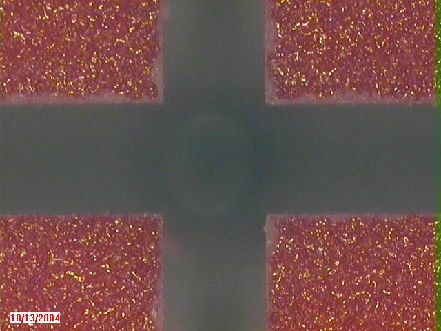
26 Dicing Thick Glass Filters Application Test - # 6 Substrate: Material: Glass filters Substrate size: - 50x 50mm [2 x 2 ]. Thickness: - 6mm - [.236 ] Saw being used: - ADT / 4 Process: Mounting:- Wax on glass Blade matrix:- ADT Sintered/ENGS- I06 Blade O.D.:- 4.6 Blade thickness:-.020 Blade exposure:- 7.65mm Diamond grit:- 80mic. Blade P/N:- 4B777-ENGS-I06 Cutting parameters: Spindle:- 7.5Krpm Feed rate: mm/sec Cut depth:- 2 steps, #1-2mm no. #2-4.25mm 0.25mm into the base glass Coolant:- Tap water with Universal Photonics Blue cool coolant additive at a 0.5%. Cooling nozzle 2.5mm x 2.5l/min. Customer spec: Top & back side chipping:- <.500mm Perpendicularity (degree):- +/ Kerf:- Not critical / it is trimming only
27 Dicing Thick Glass Filters Dressing: New Blade * On line dressing Dressing media Silicon carbide Silicon carbide 320 mesh 320 mesh P/N P/N Spindle speed 7500rpm 7500rpm Feed rate 5mm/sec 5mm/sec No. of cuts 5 5 Cut depth 0.6mm 1mm Into the board * On line dressing was performed after 10x cuts


28 Dicing Thick Glass Filters Dicing result: Top & back side chipping Top side chipping Back side chipping
29 Dicing Thick Glass Filters Scale 1:8


30 PCB - LED Package PCB LED package


31 PCB - LED Package PCB LED package Cut Quality Good cut quality Burrs


32 PCB - LED Package PCB LED package -Blade Characteristics 2 Nickel serrated T, V, Z Diamond grit size: 10,13,17 microns Thickness: Cutting Parameters Feed rate: mm/sec Spindle speed: 2 : krpm 4 : krpm
33 Alumina - Hybrids Alumina- Hybrids -Blade Characteristics 2, 4 Resin types K & R Diamond grit size: microns Thickness: (0.15mm 0.3mm) -Cutting Parameters Feed rate: 4-20 mm/sec Spindle speed: 2 : krpm 4 : krpm

 -Cutting Parameters Feed rate: 2-10 mm/sec Spindle")
34 Quartz SAW Filters Quartz - SAW Filters -Blade Characteristics 2, 4 Resin type Q & K Diamond grit size: microns Thickness: (0.15mm 0.3mm) -Cutting Parameters Feed rate: 2-10 mm/sec Spindle speed: 2 : krpm 4 : 8-16 krpm
35 BGA BGA Small package with large number of communication ports Good heat conducting due to large contact surface Operate in low electrical current and high frequencies. Easy handling with ball shaped and not pins Notebook computers Personal Digital Assistants (PDAs) Mobile telephones High density disk drives Camcorders Digital cameras


36 BGA BGA Quality Criteria Quality Criteria Chipping copper traces

37 BGA BGA Quality Criteria Burr Top View copper traces


38 BGA BGA Quality Criteria Package Size Copper tracers short copper traces

39 BGA BGA Quality Criteria Market Requirements Chipping: < 50 mm Burrs: < 50 mm No copper trace shorts Package size: Nominal +/- 50 mm Package symmetry: <100 mm


40 BGA BGA Wear Mechanism effect Hard Blade Soft Blade Low radial wear Blade thickness is reduced faster Shorter blade life - package size Higher radial wear Blade thickness is reduced slower Longer blade life - package size
41 BGA BGA -Blade Characteristics Metal Sintered blade Diamond grit size: microns Thickness: (0.2mm 0.350mm) -Cutting Parameters Feed rate: mm/sec Spindle speed: 2 : krpm 3 : krpm

 Cutting Parameters Feed rate: 1-3 inch/sec Spindle")
42 Silicon Wafers Silicon Low cost Semiconductor Devices Blade Characteristics Nickel - Hub / Hub less Diamond grit: 2/4 up to 4/8 microns Thickness: (0.02mm 0.035mm) Cutting Parameters Feed rate: 1-3 inch/sec Spindle speed: krpm


43 LTCC LTCC Quality Criteria Chipping 30µ - 50µ

44 LTCC LTCC -Blade Characteristics 2 Sintered & Resinoid type Q & K Diamond grit size: Sintered: microns Resinoid: microns Thickness: (0.2mm 0.5mm) -Cutting Parameters Feed rate: 5-25 mm/sec Spindle speed: krpm
 Diamond")

45 PZT Ultrasound Sensors PZT Ultrasound Sensors Blade Characteristics 2 Nickel - Hub less (Some hub blades) Diamond grit size: 3-6 up to 10 microns Thickness: (0.02mm 0.1mm) Cutting Parameters Feed rate: 1-6 mm/sec Spindle speed: krpm

 Cutting Parameters Feed rate: 1-10 mm/sec Spindle")
46 Ink jet Print Heads Ink Jet Print Heads Blade Characteristics 2 Nickel - Hub / Hub less Diamond grit size: 2/4 10 microns Thickness: (0.02mm 0.1mm) Cutting Parameters Feed rate: 1-10 mm/sec Spindle speed: krpm

 -Cutting Parameters Feed rate: 50-250 mm/sec")
47 MLC Multi Layer Ceramic Capacitors -Blade Characteristics 4 Nickel & Nickel Steel Core Diamond grit size: microns Thickness: (0.15mm 0.35mm) -Cutting Parameters Feed rate: mm/sec Spindle speed: krpm

 -Cutting Parameters Feed rate: Slicing: 1-5 mm/sec Parting 1-10")
48 Magnetic Heads Altec AlTiCO3- Magnetic Heads -Blade Characteristics 4 Sintered, Nickel Diamond grit size: Sintered: microns Nickel: 2/4-15 microns Thickness: (0.075mm 0.25mm) -Cutting Parameters Feed rate: Slicing: 1-5 mm/sec Parting 1-10 mm/sec Spindle speed: 8-12 krpm.

 -Cutting Parameters Feed rate: 4-20 mm/sec Spindle")
49 Alumina Alumina- Hybrids -Blade Characteristics 2, 4 Resin types K & R Diamond grit size: microns Thickness: (0.15mm 0.3mm) -Cutting Parameters Feed rate: 4-20 mm/sec Spindle speed: 2 : krpm 4 : krpm

 -Cutting Parameters Feed rate: 4-20 mm/sec Spindle speed:")
50 Ceramic BGA Ceramic BGA -Blade Characteristics Resin types K & R Diamond grit size: 45, 53, 63 microns Thickness: (0.2mm 0.5mm) -Cutting Parameters Feed rate: 4-20 mm/sec Spindle speed: 2 : krpm 3 : krpm 4 : krpm
51 QFN SINGULATION
52 QFN Singulation Package foundries are demanding process solutions to reduce Cost of Ownership, while maintaining product Quality
53 QFN Singulation Copper Lead Frame N. Palladium or Tin (Sn) coated ~ 1 mm Various moldings & fillers Various pattern designs Various copper coatings Composite Materials

54 QFN Singulation Mold Cu Plastic Deformation
 Standard - HE (Half Etched) - 0.8-1.2mm (up to 200 mic.")
 Two different Types of Coating: Tin (Sn) causing melting")
55 QFN Families Three main family types: Power - Largest thickness mm (~ 500 mic. copper lead thickness) Standard - HE (Half Etched) mm (up to 200 mic. copper lead thickness) Thin mm (up to 150 mic. copper lead thickness) Two different Types of Coating: Tin (Sn) causing melting Ni/Pd larger Y burrs SN coating melting


56 QFN Singulation Copper lead Molding Free Edge Half etching process Composite material

 -Cutting Parameters Feed rate: Half Etched: 30-100 mm/sec Full")
57 QFN - Blade and Cutting Parameters -Blade Characteristics New Resinoid types E & T Diamond grit size: microns Thickness: (0.2mm 0.5mm) -Cutting Parameters Feed rate: Half Etched: mm/sec Full Copper: mm/sec Spindle speed: 2 : krpm 3 : krpm

58 Substrate matrix Copper Molding Throughput Feed rate QFN Singulation QFN / MLP SINGULATION Life Blade De-lamination Melting on Sn Chipping Quality Burrs Smearing Factors affecting the cutting results
59 QFN Singulation Characteristic Blade life Feed rate Coolant Current Status meter mm/sec D.I. & Additive & Chiller Market Status


60 QFN Singulation Side Burrs Molding Chipping Top Burrs Smearing Quality Criteria
61 QFN Singulation 0.100mm 0.025mm Continuous chipping 0.050mm max 0.050mm max Top view Cross section Specification limits may vary between end-users Chipping Specification

62 QFN Singulation X- Burr Z- Burr Y- Burr Copper Smearing 25% of lead to lead distance Burr & Smearing Geometry Lead to Lead Distance Lead Molding Cross Section
63 QFN Singulation 0.050mm max mm max. Burr Width Burr height Top view Cross section Specification limits may vary between end-users Burrs Specification
64 QFN Singulation - X- Burr mm max mm max No Lead Delaminating. No Lead Removal. Top view Specification limits may vary between end-users X - Burrs Specification
65 QFN Singulation General Rules Smearing < 25 % of lead pitch No lead de-lamination No lead removal 25% of pitch Pitch Cross section Specification limits may vary between endusers Smearing Specification
66 QFN Singulation Tape process: First index Dicing sequence to minimize load Second index

67 QFN Singulation Tapeless process: 3rd index First index 2nd index 4th index Dicing sequence to minimize load
68 E & T Type Resin Blades for QFN Best Cost of Ownership Better blade life (Exceeding 1000 m) Above average cut quality Better throughput Wear um / meter QFN Application 30 mm/sec 50 mm/sec 70 mm/sec 100 mm/sec 20 0 RFP E03 E01 E06 T04 Matrix Type
69 Recommended Values Product Material Blade Selection & Process Parameters Blade Blade Matrix Diamond size Spindle Speed Feed Rate Type O.D mic KRPM mm/s Inch/s PBGA Epoxy & Molding Sintered / Nickel 2" Tape: hard 2": , 40, 50 3" Tape-less: Soft 3": CBGA Alumina & Molding Resin 2" KUP, RUP 45, 53, 63 2": " 4": QFN Copper & Molding Resin 2" "E" type ": " 3": PCB FR4 / Epoxy & Copper Nickel 2" "T", "V", "Z" 10, 13, 17 2": " 4": Ceramic Packages Multi Layer Capacitor Alumina Green Ceramic Resin 2" KUP, RUP 45, 53, 63, " Nickel / Nickel Steel Core 4" Hard 30, 50,
70 Recommended Values (cont.) Product Ultrasound Sensors / Ink Jet Print Head Blade Selection & Process Parameters Blade Blade Matrix Diamond size Spindle Speed Type O.D mic KRPM mm/s Inch/s PZT Nickel 2" Medium - Hard 2-4, 4-8, IC Silicon Nickel 2" Medium - Hard 2-4, 4-6, Active Devices (Discrete) Optical and Electro- Optics components Fiber Optics components Fiber Optics components Fiber Optics components SAW Devices SAW Devices Material GaAs Nickel 2" Medium - Hard 1-3, Sapphire Quartz Glass / Fused Silica Si On Glass Quartz LiNbO3 ; LiTaO3 Resin Resin Resin Resin Resin Nickel / Resin 2" QIP, QKP, QUP 45, 53, 63 4" " QIP, QKP, QUP 25, 30, 45, 53 4" " QIP, QKP, QUP " " QIP, QKP, QUP 2-4, 3-6, 9, 15, Feed Rate " "Q" Type, KUP 25, 30, 45, " 8-16 Nickel: 4-8 2" "Q" Type, KUP Resin: 9,15,20,30
71 Recommended Values (cont.) Product Tape Head Material Ferrite Blade Selection & Process Parameters Blade Blade Matrix Diamond size Spindle Speed Type O.D mic KRPM mm/s Inch/s Resin / Nickel 2" Nickel: Med - Hard ; Resin: QUP,KUP,RUP Nickel: 3-6, 4-8, 10, 17 Resin: 9, 15, 20, Feed Rate Magnetic Heads Passive & Active Devices SAW Devices, RF TiC LTCC HTCC Sintered / Nickel Sintered / Resin Sintered / Resin 4" 2" 2" Medium - Hard Sintered: Various Resin "Q" & "K" types Sintered: Soft Resin "Q" & "K" types Sintered: 10,17,20 Slicing: Nickel: 2-4,3-6,10,15 Sintered: Parting: ,25,30,35 ; Resin: 15,20,25,30 Sintered: 30,35,40,45 ; Resin: 20-45
72 Blade Selection Resin matrix types Resin type Q QIP QKP QUP Cut Quality Cut Quality K R E KIP KKP KUP RUP RFP E03 E01 E06 Blade life T T04 T06 C C03 C02 Blade life
Pushing and Entering
 Pushing and Entering Dressed Blades versus Non Dressed Blades High loads Low diamond exposure Low machinability High diamond exposure High machinability Blade Edge Grinding Blade Silicon Carbide wheel
Nickel-bond Blades The best choice for soft material and machinable hard material applications
 Nickel-bond Blades The best choice for soft material and machinable hard material applications A Comprehensive Dicing Solution The hardest binder for superior wear resistance The thinnest blade available
Dicing Products. Hub Blades and Services for Advanced Material Applications
 Dicing Products Hub Blades and Services for Advanced Material Applications In the last two years, the implementation of new and significant quality improvement processes, combined with the addition of
A W I D E S E L E C T I O N O F B L A D E S F O R A VA R I E T Y O F D I C I N G A P P L I C AT I O N S. Resin-bond Blades
 A W I D E S E L E C T I O N O F B L A D E S F O R A VA R I E T Y O F D I C I N G A P P L I C AT I O N S Resin-bond Blades The best choice for hard and brittle material applications A Comprehensive Dicing
Resin. Bond Blade DICING CONSUMABLES APPLICATION SPECIFICATIONS SD BA 56D 0.1T 40H SELF-SHARPENING
 Resin Blade Resin bond blade, with the characteristic of freecutting and selfsharpening, can efficiently improve cut quality and efficiency on ductile and gmy materials such as QFNs and coppers and on
Abstract. Introduction
 Accelerating Silicon Carbide Power Electronics Devices into High Volume Manufacturing with Mechanical Dicing System By Meng Lee, Director, Product Marketing and Jojo Daof, Senior Process Engineer Abstract
Die Attach Materials. Die Attach G, TECH. 2U. TECHNICAL R&D DIV.
 Die Attach Materials Die Attach G, TECH. 2U. TECHNICAL R&D DIV. 2 Topics 3 What it is X 5,000 X 10,000 X 50,000 Si Chip Au Plating Substrate Ag Resin 4 Current Products Characteristics H9890-6A H9890-6S
RF System in Packages using Integrated Passive Devices
 RF System in Packages using Integrated Passive Devices by Kai Liu, YongTaek Lee, HyunTai Kim, Gwang Kim, and Billy Ahn STATS ChipPAC 1711 W. Greentree Drive, Suite #117, Tempe, AZ 85284, USA Tel: 480-222-1722
Simulation of Embedded Components in PCB Environment and Verification of Board Reliability
 Simulation of Embedded Components in PCB Environment and Verification of Board Reliability J. Stahr, M. Morianz AT&S Leoben, Austria M. Brizoux, A. Grivon, W. Maia Thales Global Services Meudon-la-Forêt,
APPLICATIONS. (229mm) (254mm) (305mm) (355mm) PRODUCT NUMBERS PRODUCT DETAILS
 (254mm) (305mm) (355mm) PRODUCT NUMBERS PRODUCT DETAILS") The first step in metallographic sample preparation consists in sectioning a sample from a larger given piece to obtain a representative crosssection. Sectioning a material without causing structural changes
The first step in metallographic sample preparation consists in sectioning a sample from a larger given piece to obtain a representative crosssection. Sectioning a material without causing structural changes
Chips Face-up Panelization Approach For Fan-out Packaging
 Chips Face-up Panelization Approach For Fan-out Packaging Oct. 15, 2015 B. Rogers, D. Sanchez, C. Bishop, C. Sandstrom, C. Scanlan, TOlson T. REV A Background on FOWLP Fan-Out Wafer Level Packaging o Chips
DITF ToolKit 1. Standard Substrate Sizes (selected at the factory for optimum process)
") DITF ToolKit 1 DITF Toolkit Substrates Common Substrate Materials Alumina (99.5% min) єr = 9.9 Tan d = 1.5 x10⁻⁴ Aluminum Nitride (K170) єr = 8.9 Tan d = 2.0 x10⁻³ Beryllia (99.5%) єr = 6.7 Tan d = 3.0
DITF ToolKit 1 DITF Toolkit Substrates Common Substrate Materials Alumina (99.5% min) єr = 9.9 Tan d = 1.5 x10⁻⁴ Aluminum Nitride (K170) єr = 8.9 Tan d = 2.0 x10⁻³ Beryllia (99.5%) єr = 6.7 Tan d = 3.0
PDF created with FinePrint pdffactory Pro trial version
 Benefits Damage-free dicing of thin silicon Capable of producing smallest street widths which in return provides additional space for more parts per wafer Single step process results in reduction of cost
Challenges of Fan-Out WLP and Solution Alternatives John Almiranez
 Challenges of Fan-Out WLP and Solution Alternatives John Almiranez Advanced Packaging Business Development Asia Introduction to Fan-Out WLP Introduction World of mobile gadgetry continues to rapidly evolve
MECHANICAL MICROMACHINING OF HIGH ASPECT RATIO MICRO-STRUCTURES
 MECHANICAL MICROMACHINING OF HIGH ASPECT RATIO MICRO-STRUCTURES Hans H. Gatzen, Caspar Morsbach, Alexey Karyazin Institute for Microtechnology, Hanover University, Germany Key Words: precision machining,
Sample Preparation Techniques (Theory & Applications)- Microsectioning Technology, Metallography
- Microsectioning Technology, Metallography") Sample Preparation Techniques (Theory & Applications)- Microsectioning Technology, Metallography Introduction: Challenges of Microelectronic Cross-Sectioning Complexities of Modern Microelectronics Planning
Sample Preparation Techniques (Theory & Applications)- Microsectioning Technology, Metallography Introduction: Challenges of Microelectronic Cross-Sectioning Complexities of Modern Microelectronics Planning
Superabrasives Products. Solutions for Industry
 Superabrasives Products Solutions for Industry www.master-abrasives.co.uk Introduction Master Abrasives Master Abrasives has a hard and long earned reputation in the UK abrasives market for providing solutions
Flap wheels The pro for flexible stock removal
 The pro for flexible stock removal TRUST BLUE Abrasive solutions with high stock removal Application specific design for high flexibility Comprehensive range provides solutions for different applications
PRECISION MACHINING & FINISHING. Micron+ NE X T GENERATION MICRON+
 PRECISION MACHINING & FINISHING NE X T GENERATION MICRON+ Toolmakers can achieve highly consistent engineered abrasive tools using, which increases productivity and dramatically improves workpiece quality.
Satisfaction APPLIED LASER TECHNOLOGY, INC. APPLIED LASER TECHNOLOGY, INC.
 Satisfaction C o m m e n t s f r o m ALT is the best supplier on my approved vendor list. I ve worked with ALT for over 20 years and I can always count on quick response and A+ quality. O u r C u s t o
Rockwell R RF to IF Down Converter
 Construction Analysis Rockwell R6732-13 RF to IF Down Converter Report Number: SCA 9709-552 Global Semiconductor Industry the Serving Since 1964 17350 N. Hartford Drive Scottsdale, AZ 85255 Phone: 602-515-9780
Preface Preface to First Edition
 Contents Foreword Preface Preface to First Edition xiii xv xix CHAPTER 1 MEMS: A Technology from Lilliput 1 The Promise of Technology 1 What Are MEMS or MST? 2 What Is Micromachining? 3 Applications and
RO4835T Core/RO4450T Bonding Layers Multi-Layer Board Processing Guidelines
 Fabrication Technical Articles Notes RO4835T Core/RO4450T Bonding Layers Multi-Layer Board Processing Guidelines These guidelines were developed to provide fabricators basic information on processing core
Enabling Technology in Thin Wafer Dicing
 Enabling Technology in Thin Wafer Dicing Jeroen van Borkulo, Rogier Evertsen, Rene Hendriks, ALSI, platinawerf 2G, 6641TL Beuningen Netherlands Abstract Driven by IC packaging and performance requirements,
Mounted Points Mounted Points
 Mounted Points I 1 iamond and CBN ools 205 Mounted Points able of Contents ool drive Contents Page General information 3 he fast way to the best tool 4-5 Ordering instructions 6 Mounted points Hardness
UNCONVENTIONAL MACHINING PROCESS UNIT 1 INTRODUCTION. Prepared by S. SENTHIL KUMAR AP / MECH SVCET
 UNCONVENTIONAL MACHINING PROCESS UNIT 1 INTRODUCTION Prepared by S. SENTHIL KUMAR AP / MECH SVCET INTRODUCTION Conventional machining process Metal is removed by means of tool which is harder than work
Masterflex Polishing Products
 Masterflex Polishing Products How to Order Masterflex Polishing Products When ordering it is important to give as much information about the operation as possible so that the correct grading is supplied.
Mounted Points Mounted Points
 Mounted Points I 1 iamond and CBN ools 205 Mounted Points able of Contents ool drive Contents Page General information 3 he fast way to the best tool 4-5 Ordering instructions 6 Mounted points Hardness
Polymer Microfabrication (Part II) Prof. Tianhong Cui, Mechanical Engineering ME 8254
 Prof. Tianhong Cui, Mechanical Engineering ME 8254") Polymer Microfabrication (Part II) Prof. Tianhong Cui, Mechanical Engineering ME 8254 Other Polymer Techniques Embossing Low cost High throughput Structures as small as 25 nm Injection molding Features
Polymer Microfabrication (Part II) Prof. Tianhong Cui, Mechanical Engineering ME 8254 Other Polymer Techniques Embossing Low cost High throughput Structures as small as 25 nm Injection molding Features
LMP s Contributions in Manufacturing Process Research. September 28, 2007
 LMP s Contributions in Manufacturing Process Research September 28, 2007 Outline Introduction Selective Examples Summary Introduction Founded as an interdepartmental laboratory within the School of Engineering
> RX12UF. Cobalt content w/w. Grade. Properties and recommendations. HARTMETALL ESTECH AG 6285 Hitzkirch
 pli > Ultra-fine grain carbides are characterized by a very high hardness and wear resistance. They are used for milling tools and drills for processing abrasive, soft and tough materials, in nozzles and
Cutting Tool Materials and Cutting Fluids. Dr. Mohammad Abuhaiba
 Cutting Tool Materials and Cutting Fluids HomeWork #2 22.37 obtain data on the thermal properties of various commonly used cutting fluids. Identify those which are basically effective coolants and those
Device Attachment Methods and Wirebonding Notes for RT/duroid and RO4000 Series High Frequency Laminates
 Device Attachment Methods and Wirebonding Notes for RT/duroid and RO4000 Series High Frequency Laminates Volume production of microwave circuit assemblies requires fast, reliable and efficient methods
Polishing-, Ceramic Stones & Accessories
 Polishing-, Ceramic Stones & Accessories 5 a company A COMPANY Content Polishing-, Ceramic Stones & Accessories 5 Polishing-, Ceramic Stones & Accessories Polishing Stones...2 Ceramic Stones...16 Super
microdice System for Separation of SiC Wafer Using Thermal Laser Separation
 microdice System for Separation of SiC Wafer Using Thermal Laser Separation - System Integration Technologies Fraunhofer ENAS - (Ronny Neubert, 3D-Micromac AG) 3D-Micromac At a Glance Manufacturer and
Best Practice Guide for Thermocycling and Reliability Assessment of Solder Joints
 Best Practice Guide for Thermocycling and Reliability Assessment of Solder Joints Miloš Dušek and Christopher Hunt July 2000 July 2000 Best Practice Guide for Thermocycling and Reliability Assessment of
Dicing of Ultra-thin Silicon Wafers
 Dicing of Ultra-thin Silicon Wafers Hans H. Gatzen, Gerald Guenzel Institute for Microtechnology, Hanover University, Germany Keywords: dicing, ultra thin wafers, silicon, chipping, machining Abstract:
Low CTE / High Tg FR-4 with High Heat Resistance
 Low CTE / High Tg FR-4 with High Heat Resistance Laminate: EM-827 Prepreg: EM-827B 1 Features Tg(DSC) > 170 Z direction CTE < 3.0% (50~260 ) High thermal degradation temperature: Td > 340 Excellent thermal
Polycrystalline diamond blanks and cut shapes for inserts and round tools. TOOLMAKER SOLUTIONS Compax PCD Tool Blanks and Inserts
 Polycrystalline diamond blanks and cut shapes for inserts and round tools TOOLMAKER SOLUTIONS Compax PCD Tool Blanks and Inserts COMPAX PCD PRODUCT OFFERINGS Hyperion offers a vast selection of superior
Mounted points. Table of contents. Hardness R for foundries Cylindrical ZY 35 Tree SP 35 Tapered KE 36
 Fine grinding and polishing tools iamond and CBN tools 204 205 Mounted points able of contents Contents Page General information 3 he fast way to the best tool 4 Ordering instructions 6 Extensions for
CX Thin Fil s. Resistors Attenuators Thin-Film Products Thin-Film Services. ISO 9001:2008 RoHS/REACH Compliant ITAR Compliant
 CX Thin Fil s Resistors Attenuators Thin-Film Products Thin-Film Services www.cxthinfilms.com ISO 9001:2008 RoHS/REACH Compliant ITAR Compliant www.cxthinfilms.com sales@cxthinfilms.com +1 (401) 461-5500
Hot Chips: Stacking Tutorial
 Hot Chips: Stacking Tutorial Choon Lee Technology HQ, Amkor Enabling a Microelectronic World Mobile Phone Technology Change Feature Phone Smartphone Smartphones as a Percentage of All Phones Source : The
Wafer Level Molded DDFN Package Project Duane Wilcoxen
 Wafer Level Molded DDFN Package Project Duane Wilcoxen Definition of DDFN (Encapsulated CSP) DDFN package basically is a CSP device with an epoxy coating on all (or most) of the device sides for added
ANALYSING BACKSIDE CHIPPING ISSUES OF THE DIE AT WAFER SAW. Martin Vagues In Partial Fulfillment of MatE 234 May 10th, 2003
 ANALYSING BACKSIDE CHIPPING ISSUES OF THE DIE AT WAFER SAW Martin Vagues In Partial Fulfillment of MatE 234 May 10th, 2003 Prof Gunaselvaduray SJSU, San Jose ABSTRACT With shrinking technologies evolving,
Close supply chain collaboration enables easy implementation of chip embedded power SiP
 Close supply chain collaboration enables easy implementation of chip embedded power SiP Gerald Weidinger, R&D Project Leader, AT&S AT & S Austria Technologie & Systemtechnik Aktiengesellschaft Fabriksgasse13
LTCC SYSTEMS and LTCC DESIGN RULES
 LTCC SYSTEMS and LTCC DESIGN RULES Low Temperature Co-fired Ceramic revision status: G page 1 of 19 Table of Contents: 1 General page 3 2 Commercial LTCC tape systems page 4 3 Design possibilities page
GRINDING AND OTHER ABRASIVE PROCESSES
 GRINDING AND OTHER ABRASIVE PROCESSES Grinding Related Abrasive Process Abrasive Machining Material removal by action of hard, abrasive particles usually in the form of a bonded wheel Generally used as
Polycrystalline diamond blanks and cut shapes for inserts and round tools. TOOLMAKER SOLUTIONS Compax PCD Tool Blanks and Inserts
 Polycrystalline diamond blanks and cut shapes for inserts and round tools TOOLMAKER SOLUTIONS Compax PCD Tool Blanks and Inserts COMPAX PCD PRODUCT OFFERING Hyperion offers a vast selection of superior
Packaging Technologies for SiC Power Modules
 Packaging Technologies for SiC Power Modules Masafumi Horio Yuji Iizuka Yoshinari Ikeda ABSTRACT Wide bandgap materials such as silicon carbide (SiC) and gallium nitride (GaN) are attracting attention
Lattice isplsi1032e CPLD
 Construction Analysis Lattice isplsi1032e CPLD Report Number: SCA 9612-522 Global Semiconductor Industry the Serving Since 1964 15022 N. 75th Street Scottsdale, AZ 85260-2476 Phone: 602-998-9780 Fax: 602-948-1925
Piezoelectric Polycrystalline (PZT) Components and Wafers
 Components and Wafers") Piezoelectric Polycrystalline (PZT) Components and Wafers Industry Leading Piezoelectric Polycrystalline (PZT) Component Manufacturing and Engineering CTS offers high-performance piezoelectric materials
Piezoelectric Polycrystalline (PZT) Components and Wafers Industry Leading Piezoelectric Polycrystalline (PZT) Component Manufacturing and Engineering CTS offers high-performance piezoelectric materials
IMPLEMENTATION OF A FULLY MOLDED FAN-OUT PACKAGING TECHNOLOGY
 IMPLEMENTATION OF A FULLY MOLDED FAN-OUT PACKAGING TECHNOLOGY B. Rogers, C. Scanlan, and T. Olson Deca Technologies, Inc. Tempe, AZ USA boyd.rogers@decatechnologies.com ABSTRACT Fan-Out Wafer-Level Packaging
ANCA > How to run a Grinding Test
 ANCA > How to run a Grinding Test How to run a Grinding Test Often, the full potential of grinding wheels is not completely utilised. This may be due to a lack of systematic approach. The following describes
Fine Pitch P4 Probe Cards
 Fine Pitch P4 Probe Cards Photolithographic Pattern Plating Process June 1998 By Toshi Ishii, Hide Yoshida Contents What is a P4 probe card? Specification Some test results Tip cleaning RF performance
Additive Manufacturing Technology
 Additive Manufacturing Technology ME 012193 Spring I 2018 By Associate Prof. Xiaoyong Tian Cell:13709114235 Email: leoxyt@mail.xjtu.edu.cn Lecture 02 Fundmental AM processes Interactions in AM processes
Leveraging the Precision of Electroforming over Alternative Processes When Developing Nano-scale Structures
 VOLUME 4 - ELECTROFORMING Leveraging the Precision of over Alternative Processes When Developing Nano-scale Structures Electrical and mechanical component and subsystem designers generally have five techniques
Plasma for Underfill Process in Flip Chip Packaging
 Plasma for Underfill Process in Flip Chip Packaging Jack Zhao and James D. Getty Nordson MARCH 2470-A Bates Avenue Concord, California 94520-1294 USA Published by Nordson MARCH www.nordsonmarch.com 2015
The Many Facets and Complexities of 316L and the Effect on Properties
 The Many Facets and Complexities of 316L and the Effect on Properties Ingrid Hauer Miller Höganäs AB, Höganäs, Sweden state and country Ingrid.hauer@hoganas.com, +46702066244 Abstract One of the most widely
Tribology Advanced Scratch Testing Applications -Suresh Kuiry, Ph.D.
 Tribology 101 - Advanced Scratch Testing Applications -Suresh Kuiry, Ph.D. Introduction Scratch Test - Introduction Various Types of scratch tests Brief description of Bruker UMT- Scratch Test Module Deciding
I. Overview. General Considerations
 I. Overview Thru-feed grinders offer an economical means to surface grind small parts in an efficient manner. There are several different models of these grinders available, though the Speedfam Thru-Feed
10 Manor Parkway, Suite C Salem, New Hampshire
 Micro-Precision Technologies (MPT) is an independent manufacturer of hybrid integrated circuits, multichip modules, and high-precision thick film substrates for the military, medical, avionics, optoelectronics,
Freescale Semiconductor Tape Ball Grid Array (TBGA) Overview
 Overview") Freescale Semiconductor Tape Ball Grid Array (TBGA) Overview Revision 0 2006 Freescale and the Freescale logo are trademarks of Freescale Semiconductor, Inc. All other product or service names are the
Freescale Semiconductor Tape Ball Grid Array (TBGA) Overview Revision 0 2006 Freescale and the Freescale logo are trademarks of Freescale Semiconductor, Inc. All other product or service names are the
ADVANCES in NATURAL and APPLIED SCIENCES
 ADVANCES in NATURAL and APPLIED SCIENCES ISSN: 1995-0772 Published BY AENSI Publication EISSN: 1998-1090 http://www.aensiweb.com/anas 2016 April 10(4): pages 436-441 Open Access Journal Development of
Chapter 2 Manufacturing Process
 Digital Integrated Circuits A Design Perspective Chapter 2 Manufacturing Process 1 CMOS Process 2 CMOS Process (n-well) Both NMOS and PMOS must be built in the same silicon material. PMOS in n-well NMOS
3D Package Technologies Review with Gap Analysis for Mobile Application Requirements. Apr 22, 2014 STATS ChipPAC Japan
 3D Package Technologies Review with Gap Analysis for Mobile Application Requirements Apr 22, 2014 STATS ChipPAC Japan T.Nishio Contents Package trends and roadmap update Advanced technology update Fine
1 Cutting Tool Materials of common use
 1 Cutting Tool Materials of common use Instructional Objectives At the end of this lesson, the students will be able to (i) Identify the needs and cite the chronological development of cutting tool materials.
Introduction of CSC Pastes
 Introduction of CSC Pastes Smart Phones & Conductive Pastes Chip Varistors Chip Inductors LC Filters Flexible Printed Circuit Boards Electronic Molding Compounds ITO Electrodes PCB Through Holes Semiconductor
Keeping the Customer First. Tungaloy Catalogue TE0707-E2. Cutting Tools.
 Keeping the Customer First Tungaloy Catalogue TE0707-E2 2007 Cutting Tools www.tungaloy-eu.com Selection Guides List of... 410 Selection Guides... 412 Specifications Solid Carbide s For High Speed Deep
Ceramic and glass technology
 1 Row materials preperation Plastic Raw materials preperation Solid raw materials preperation Aging wet milling mastication Mixing seving Grain size reduction Milling Crushing Very fine milling Fine milling
Meso A/SMP Approach. Abstract
 Abstract Additive/Subtractive Material Processing for Mesoscopic Parts Yih-Lin Cheng, Jurgen Stampfl, Rudolf Leitgeb, and Fritz B. Prinz Stanford University, Stanford, CA Mesoscopic additive/subtractive
KGC SCIENTIFIC Making of a Chip
 KGC SCIENTIFIC www.kgcscientific.com Making of a Chip FROM THE SAND TO THE PACKAGE, A DIAGRAM TO UNDERSTAND HOW CPU IS MADE? Sand CPU CHAIN ANALYSIS OF SEMICONDUCTOR Material for manufacturing process
Material based challenge and study of 2.1, 2.5 and 3D integration
 1 Material based challenge and study of 2.1, 2.5 and 3D integration Toshihisa Nonaka Packaging Solution Center R&D Headquarters Hitachi Chemical Co., Ltd., Sep. 8, 2016 Hitachi Chemical Co., Ltd. 2010.
PCD Tools Specification and Application Zhengzhou Halnn Superhard Materials Co.Ltd
 PCD Tools Specification and Application Zhengzhou Halnn Superhard Materials Co.Ltd www.halnncbn.com Definition of PCD Polycrystalline Diamond(PCD) refers to the polycrystalline which is obtained by mixing
Challenges for Embedded Device Technologies for Package Level Integration
 Challenges for Embedded Device Technologies for Package Level Integration Kevin Cannon, Steve Riches Tribus-D Ltd Guangbin Dou, Andrew Holmes Imperial College London Embedded Die Technology IMAPS-UK/NMI
Harder. Faster. Yellow. The new Kronenflex cutting-off wheels
 Harder. Faster. Yellow. The new Kronenflex cutting-off wheels Nothing can beat good, solid tools For us, as the inventor of high-speed cutting-off wheels, it goes without saying that we are interested
Lasers in Advanced Packaging
 Lasers in Advanced Packaging Xiangyang Song, Cristian Porneala, Dana Sercel, Kevin Silvia, Joshua Schoenly, Rouzbeh Sarrafi, Sean Dennigan, Eric DeGenova, Scott Tompkins, Brian Baird, Vijay Kancharla,
Content Details Page. Metal hybrid bonds SHARKLINE Resin bonds. Resin ceramic bonds Resin hybrid bonds Bakelite bonds
 1-01 GENERAL INFORMATION Content Details Page TYPE DESIGNATION Type designation like 1A1W or 6A2 explained 1-02 ENGRAVING ID number and other information 1-04 Metal bonds 1-05 Metal hybrid bonds SHARKLINE
Diamond abrasives offering customized and tailored solutions for demanding applications. TOOLMAKER SOLUTIONS MBG Diamond
 Diamond abrasives offering customized and tailored solutions for demanding applications TOOLMAKER SOLUTIONS MBG Diamond MBG DIAMOND FOR DEMANDING GRINDING APPLICATIONS Hyperion s MBG diamond offers a solution
HOW THE MOLD COMPOUND THERMAL EXPANSION OVERRULES THE SOLDER COMPOSITION CHOICE IN BOARD LEVEL RELIABILITY PERFORMANCE
 HOW THE MOLD COMPOUND THERMAL EXPANSION OVERRULES THE SOLDER COMPOSITION CHOICE IN BOARD LEVEL RELIABILITY PERFORMANCE AUTHORS: B. VANDEVELDE, L. DEGRENDELE, M. CAUWE, B. ALLAERT, R. LAUWAERT, G. WILLEMS
NTB DiaCer NTB CeraCBN
 NTB DiaCer NTB CeraCBN Diamond & CBN Grinding Wheels 1.0 Super-Abrasive Diamond and CBN Vitrified Grinding Wheels Super-Abrasive wheels play a key role in the grinding process for Advanced Ceramics, Semi-Conductor,
Technology Drivers for Plasma Prior to Wire Bonding
 Technology Drivers for Plasma Prior to Wire Bonding James D. Getty Nordson MARCH Concord, CA, USA info@nordsonmarch.com Technology Drivers for Plasma Prior to Wire Bonding Page 1 ABSTRACT Advanced packaging
Tooling for Composites and Aerospace Materials. Diamond coated, carbide and PCD tools Routers, drills, and end mills Full special design capabilities
 Tooling for Composites and Aerospace Materials Diamond coated, carbide and PCD tools Routers, drills, and end mills Full special design capabilities DIAMOND COATED DRILLS Material-specific design and sub-micron
MTS Semiconductor Solution
 MTS 0 unplanned down time Solution Lowest operating Cost Solution Energy saving Solution Equipment Fine Pitch and UPH Upgrade solution Quality & Yield Improvement Solution Reliability Enhancement Solution
Nontraditional Machining Processes
 Nontraditional Machining Processes The NTM processes can be divided into four basic categories: I. Chemical (Chemical reaction), II. Electrochemical (Electrolytic dissolution), III. Mechanical (Multipoint
Introduction to Material Science and Engineering
 Introduction to Material Science and Engineering Introduction What is materials engineering? the understanding and modification of the structure and properties of materials to improve the performance and
Manufacturing Processes 1 (MDP 114)
") Manufacturing Processes 1 (MDP 114) First Year, Mechanical Engineering Dept., Faculty of Engineering, Fayoum University Dr. Ahmed Salah Abou Taleb 1 Cutting-Tool Materials and Cutting Fluids 2 Fracture
Manufacturing Processes 1 (MDP 114) First Year, Mechanical Engineering Dept., Faculty of Engineering, Fayoum University Dr. Ahmed Salah Abou Taleb 1 Cutting-Tool Materials and Cutting Fluids 2 Fracture
Fabrication and Layout
 ECEN454 Digital Integrated Circuit Design Fabrication and Layout ECEN 454 3.1 A Glimpse at MOS Device Polysilicon Aluminum ECEN 475 4.2 1 Material Classification Insulators Glass, diamond, silicon oxide
Oki M A-60J 16Mbit DRAM (EDO)
") Construction Analysis Oki M5117805A-60J 16Mbit DRAM (EDO) Report Number: SCA 9707-545 Global Semiconductor Industry the Serving Since 1964 17350 N. Hartford Drive Scottsdale, AZ 85255 Phone: 602-515-9780
Construction Analysis Oki M5117805A-60J 16Mbit DRAM (EDO) Report Number: SCA 9707-545 Global Semiconductor Industry the Serving Since 1964 17350 N. Hartford Drive Scottsdale, AZ 85255 Phone: 602-515-9780
Anglon Tools Tools for ANGL ROTARY HANDPC Soft rubber pads available in 4 different diameters (ø 0 mm, ø mm, ø 30 mm, ø mm) are available. Pressure se
 are available. Pressure se") inimo One Anglon Tools inimo Anglon System -- Versatility & Performance inimo Anglon angle grinders, with angles of 90 and degrees, are suitable for polishing flat, curved and end surfaces. Great for areas
inimo One Anglon Tools inimo Anglon System -- Versatility & Performance inimo Anglon angle grinders, with angles of 90 and degrees, are suitable for polishing flat, curved and end surfaces. Great for areas
AN Handling and processing of sawn wafers on UV dicing tape. Document information. Sawn wafers, UV dicing tape, handling and processing
 Handling and processing of sawn wafers on UV dicing tape Rev. 2.0 13 January 2009 Application note Document information Info Keywords Abstract Content Sawn wafers, UV dicing tape, handling and processing
SGS-Thomson M28C K EEPROM
 Construction Analysis SGS-Thomson M28C64-121 64K EEPROM Report Number: SCA 9710-559 Global Semiconductor Industry the Serving Since 1964 17350 N. Hartford Drive Scottsdale, AZ 85255 Phone: 602-515-9780
Crystal Growth and Wafer Fabrication. K.Sivasankaran, Assistant Professor (Senior), VLSI Division, School of Electronics Engineering, VIT
, VLSI Division, School of Electronics Engineering, VIT") Crystal Growth and Wafer Fabrication K.Sivasankaran, Assistant Professor (Senior), VLSI Division, School of Electronics Engineering, VIT Crystal growth Obtaining sand Raw Polysilicon Czochralski Process
Crystal Growth and Wafer Fabrication K.Sivasankaran, Assistant Professor (Senior), VLSI Division, School of Electronics Engineering, VIT Crystal growth Obtaining sand Raw Polysilicon Czochralski Process
Praxair and TAFA Arc Spray Bond Wire79B
 File: Issue: Supercedes: 1.9.1.2-79B I11229 I10816 Praxair and TAFA Arc Spray Bond Wire79B Material Review: 79B wire, a unique nickel-aluminum alloy for use in arc spray systems, is available from Praxair
FLAP DISCS CERAMIC ALUMINA - PLATINUM APPLICATION GRIT SELECTION. Abrasives COARSER (GRINDING) FINER (FINISHING)
 FINER (FINISHING)") FLAP DISCS CERAMIC ALUMINA - PLATINUM Made with the latest generation German ceramic alumina material Exceptional performance on stainless steel, titanium and super alloys Faster cutting with reduced heat
FLAP DISCS CERAMIC ALUMINA - PLATINUM Made with the latest generation German ceramic alumina material Exceptional performance on stainless steel, titanium and super alloys Faster cutting with reduced heat
Mosel Vitelic MS62256CLL-70PC 256Kbit SRAM
 Construction Analysis Mosel Vitelic MS62256CLL-70PC 256Kbit SRAM Report Number: SCA 9703-499 Global Semiconductor Industry the Serving Since 1964 17350 N. Hartford Drive Scottsdale, AZ 85255 Phone: 602-515-9780
Henkel Enabling Materials for Semiconductor and Sensor Assembly. TechLOUNGE, 14 November 2017
 Henkel Enabling Materials for Semiconductor and Sensor Assembly TechLOUNGE, 14 November 2017 Content Brief HENKEL Introduction and ELECTRONICS Focus Areas Innovative Semiconductor and Sensor Assembly Solutions
NKK NR4645LQF Bit RISC Microprocessor
 Construction Analysis NKK NR4645LQF-133 64-Bit RISC Microprocessor Report Number: SCA 9707-547 Global Semiconductor Industry the Serving Since 1964 17350 N. Hartford Drive Scottsdale, AZ 85255 Phone: 602-515-9870
Three-Dimensional Molded Interconnect Devices (3D-MID)
") Jörg Frank Three-Dimensional Molded Interconnect Devices (3D-MID) Materials, Manufacturing, Assembly and Applica ons for Injec on Molded Circuit Carriers Sample Pages ISBN 978-1-56990-551-7 HANSER Hanser
Jörg Frank Three-Dimensional Molded Interconnect Devices (3D-MID) Materials, Manufacturing, Assembly and Applica ons for Injec on Molded Circuit Carriers Sample Pages ISBN 978-1-56990-551-7 HANSER Hanser
Motorola MPA1016FN FPGA
 Construction Analysis Motorola MPA1016FN FPGA Report Number: SCA 9711-561 Global Semiconductor Industry the Serving Since 1964 17350 N. Hartford Drive Scottsdale, AZ 85255 Phone: 602-515-9780 Fax: 602-515-9781
Superhard Diamond and CBN Files, Grinding Tools and Cut-Off Wheels
 Superhard iamond and CBN Files, Grinding ools and Cut-Off Wheels 2005 Superhard iamond und CBN Abrasives Advantages and Range of Applications able of contents: Pages iamond and CBN general notes on superhard