University of Minnesota Nano Center Standard Operating Procedure
|
|
|
- Christine Briggs
- 6 years ago
- Views:
Transcription


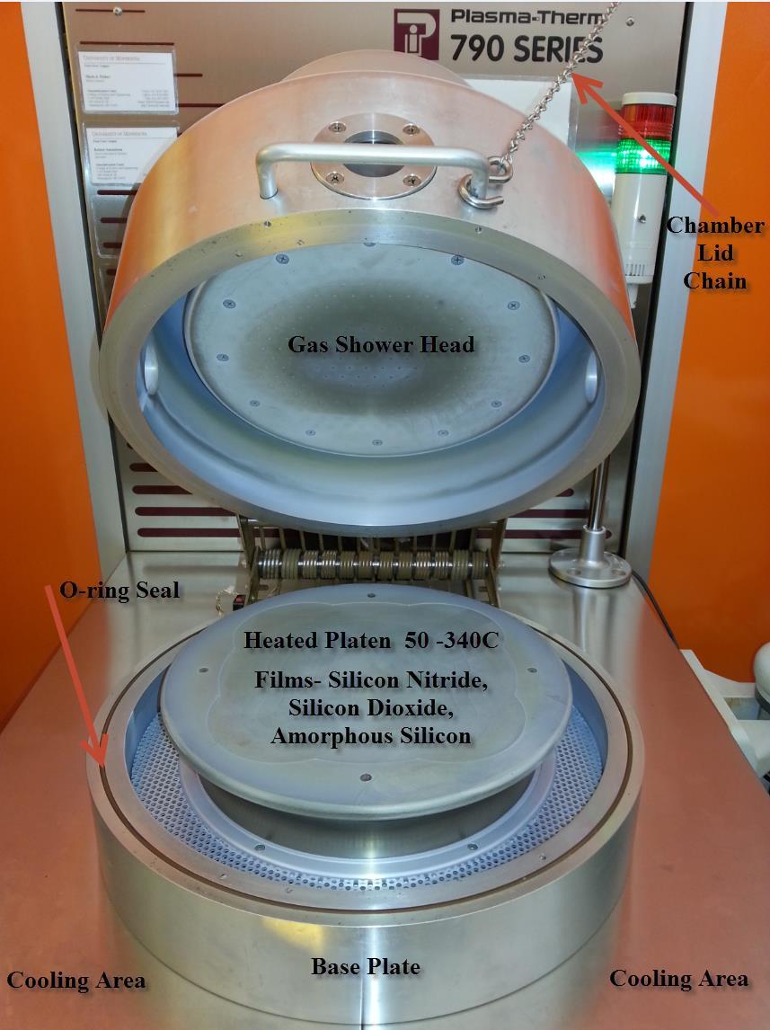
1 Equipment Name: University of Minnesota Nano Center PECVD Coral Name: pecvd Revision Number: 2.0 Model: Plasmatherm 340 Revisionist: Mark Fisher Location: Bay 3 Date: 20 Sept Description The Plasmatherm PECVD used to deposit thin films (Silicon Nitride, Silicon Dioxide, or Amorphous Silicon) from a gas state to a solid state on the substrate. The chemical reaction takes place after a RF plasma is created between the top electrode and the heated platen. The platen is heated by an embedded resistance heater with a range of degrees Celsius. This system has processes setup for the deposition of Silicon Nitride, Silicon Dioxide and Amorphous Silicon. The system processes are in located in folder c:\process. The old processes are located in folder c:\sysmon. Program naming convention is the following, SIN340.prc is Silicon Nitride at 340 C, SiO2340 is Silicon dioxide at 340 C, or ASi340 is Amorphous Silicon at 340 C. PECVD system. PECVD chamber, the gas shower head, and platen. 2 Safety The safety item beyond the normal electrical hazards is to watch out for are the platen temperatures can reach 340 degrees C. The process gases that are available in this system are N2, O2, CF4, N2O, 2%SiH4/He, NH3, and He. In the case of an Emergency press the RED EMO button and contact a MNC person about any problems. 3 Restrictions/Requirements Must be a qualified customer on the Badger and PECVD system. No Amorphous Silicon (ASi) deposition from Tuesday 12:00pm Thursday 12:00pm FYI. If you deposit SIO2, SIN, or ASi on substrates the PECVD system, those substrates may not go back into any oxide or LPCVD tubes, the except to the above is the alloy tube or RTA. Please use the 1


2 RTA in Bay 1 to denisfy the pecvd deposited film or contact a MNC staff person for additional options. 4 Required Facilities The system needs electrical power, gases, cooling water. 5 6 Definitions Process =A program that controls the sequence of events. Platen=The main base plate that the wafers or substrates are placed. Lid =The top bell jar cover of the system that opens up. 7 Setup 1. To hold your substrate in the center of the platen use 1x3 glass slides. Due to the placement of the pumping port your substrates will tend to move to the back right area of the platen. 2. It is a good idea to place a piece of bare silicon in with your process so that you can measure the thickness of your deposited film and refractive index of your deposited film. 8 Operating Instructions 1. Enable the PECVD. To enable the PECVD in Badger, first highlight the PECVD by going to Chemical Vapor Deposition>PECVD, then under Equipment Actions select Enable, the green light should now be lit. 2. Login to the system. The Operator Login window should now be in the middle of the screen. In the Operator box enter MLRE and press TAB. In the Password box enter 1234 and then click OK box. The operator name and password are in uppercase letters. The system monitor window should now be on the screen. The system monitor gives you the status of the system parameters. (The top left trackball mouse button and the roller ball are used in operation of the PECVD system). 3. Load a Process. Using the pull down menus at the top of the system monitor screen Select PROCESS>LOAD. Please change the flip card to reflect the process you are running and fill out the log book on the table. The list of process files right chamber window will appear. Check to see that the directory or folder should be c:\process. If not, change folders to c:\process. Then, highlight the process you would like to run by clicking on the name with the left hand mouse button (sin250, sin340, sio2250, sio2340, etc). The process you selected should now appear in the File Name box. Click OK in the upper right hand corner of the window. Your process should now be loaded. Check the process box for your process. 2


3 Films. The Nitride film is the cleanest film, then oxide film, while the amorphous films are the dirtiest films. So, the PECVD system should be cleaned when changing from an oxide deposition to a nitride deposition. If the last process ran was an amorphous silicon process the system should be cleaned before depositing nitride or oxide. See section 8, page 4 on cleaning the system. 4. Vent the system. Using the pull down menus at the top of the system monitor screen Select Utilities>Vent. The chamber will vent will take 1-2 minutes. The chamber lid will pop open when the chamber is vented and the pressure screen turns from vacuum (red/white) to atmosphere (blue). 5. Load your substrates. You can now lift chamber lid up by hand and load your samples or substrates. There is a chain available to hold the chamber lid open while you load your substrates. CAUTION: THE PLATEN IS VERY HOT AVOID CONTACT. Use 1x3 glass slides to hold your substrates in the center of the platen. It is possible to load four 4 wafers, one 6 wafer, or one 8 wafer. To get the best uniformity on your substrates, load them in the center of the platen, using a couple 1x3 glass slides to hold them in the center of the platen. Remember a 1x3 glass slides are 1mm thick and most substrates are thinner than 1mm, so it is best if you hold your substrate in the center of the platen with the corner of the glass slide. This loading technique will allow the gas to flow over the glass slide more uniformly, thus getting a more uniform deposition on your substrate. The way to determine the deposited film thickness and refractive index is to load a piece of bare silicon along with your substrates and measure this piece of silicon on an ellipsometer in bay 1 when your run is complete. 6. Pumping the system down. Using the pull down menus at the top of the system monitor screen Select Utilities>Pump Chamber (LoVac), while holding the chamber lid closed with a little pressure. Hold down the chamber lid until the pressure screen turns from atmosphere (blue) to vacuum (red/white). You will notice that the gap from the top lid will get smaller as the chamber pumps down. 7. To run your Process. Click on READY in the System Status cluster at the bottom of the screen. Wait until the process temperature has been reached. (Note:This could take up to 45miutes for the higher temperatures.) When the system has met all initial parameter requirements the entire READY button will turn yellow and the status bar will give the following message Ready Mode Temperature Compliance Achieved. Once the system is in the READY mode, click on RUN in the System Status cluster at the bottom of the screen. The process will now proceed 3
4 automatically steps 1-6, at step 4 you will need to stop your deposition at the correct time and advance the program to the next step by hitting the end step button during this step. See below. Step 1 Initial Pumpdoun (1 minute) Step 2 Prepurge- Important removes water vapor from the chamber. (3minutes) Step 3 Gas stabilization (2 minutes) Step 4 Process- This is the actual deposition step. (deposition time) Step 5 Postpurge- Important removes hazards gases from the chamber. (2minutes) Step 6 End and vent (3 minutes) Since most processes in c:process are written with a standard 120 minute actual deposition time (Step 4 Process) you will need to time your deposition using the clock visible in the lower right side of the screen. When the time in the Elapse box has reached the deposition time, click on the END STEP button once only in the System Status cluster at the bottom of the screen. This will end your deposition and advanced the process to the step 5. If you make a mistake and click the END STEP button more than once, wait until the system has pumped the chamber for ~30seconds, then click the ABORT button in the System Status cluster, then click-yes to abort. Select one of the following processes (Purge150, Purge250, or Purge300) select the process that is closest to your process temperature, run this process. These processes will purge the chamber of all gases and vent the system. Please see pages 7-10 for process summary sheets that include, deposition rates, stress, refractive index, etc. 8. Remove your samples. After the process is completed, the chamber will vent and the lid will open. Remove your substrates and place them on the glass plate on top of stainless steel top of the system until they cool. Cool your substrates slowly to minimize thermal shock. CAUTION: THE PLATEN AND THE SAMPLES BEING REMOVED ARE VERY HOT - USE CAUTION WHEN HANDLING. The process complete window appears stating that the process is done and the time the automatic process was completed. Click OK. If you would like to deposit on more sample go to step 5. If not, continue to next step. 9. Pump the system down. Using the pull down menus at the top of the system monitor screen. Select Utilities>Pump Chamber (LoVac), while holding the chamber lid closed. Hold down the chamber lid until the pressure screen turns from atmosphere (blue) to vacuum (red/white). You will notice that the gap from the top lid will get smaller as it pumps down. To measure the film thickness and refractive index of your samples use the ellipsometer in Bay 1. Please record this information in the log book on the table below the monitor. 10. Return the system to standby. After the system has pumped down, (the pressure box has turned white), click on the STANDBY button box in the System Status cluster at the bottom of the page. This should put the system in the STANDBY mode. 11. Logout. Click on the Utilities>Log Out. The system should now be in the STANDBY mode and logged out. 9 Cleaning the system To clean the system. choose one of the following processes clean1.prc -45minutes clean2.prc -90minutes clean3.prc-180 minutes After the clean is done, wipe out the system with Kimwipes (see image below) and then use the N2 gun to blow out the chamber from the top to bottom. Then, run your planned process for 5 to 10 min to coat the chamber with SIN or SIO2 this will help coat and seal any particles that might be left over from the cleaning process. Note:MNC Will clean the system every Tuesday morning, so the system will be ready by 12:00pm for Nitride and oxide depositions. If you have any questions please contact MNC staff. 4


5 10 Tip/Technigues Deposition Rate. The deposition rates are on the Process Summary Sheets 7-10 of this SOP. If you need your deposition to be better than X +/- 10%. It is a good idea to do a dummy run (5-10 minutes) before the actual deposition, to get a more accurate deposition rate for your run. Please put your deposition rate in the log book. Check Platen temperature. Check the system to see what the platen temperature, open the front panel door below the chamber, and the top temperature displayed should be what is in the process. See below for an example. In the photo the system is at 110 degrees and a 150 degree process was selected. 5
6 Deposition Rate. The deposition rates are on the Process Summary Sheets 7-10 of this SOP. If you need your deposition to be better than X +/- 10%. It is a good idea to do a dummy run (5-10 minutes) before the actual deposition, to get a more accurate deposition rate for your run. Please put your deposition rate in the log book. To clean the system. To run a clean process chose one of the following processes (clean1.prc (45minutes), clean2.prc (90minutes), or clean3.prc (180 minutes). After the clean is done, wipe out the system with Kimwipes (see image below) and then use the N2 gun to blow out the chamber from the top to bottom. Then, run your planned process for 5 to 10 min to coat the chamber with SIN or SIO2 this will help coat and seal any particles that might be left over from the cleaning process. To reduce pin holes in Films. Depositing more than one deposition for the total thickness, helps reduce the problems of film voids or pinholes. For example a 750 A film thickness could be split into three layers of 250 A each. This technique of depositing three layers have helped customers solve their film quality problems, to take advantage of this technique, just split your total thickness in three. Another technique customers have used is to blown off their wafers or substrates with N2 between deposition steps. 11 Problems/Troubleshooting END STEP Problem If you make a mistake and click the END STEP button more than once, wait until the system has pumped the chamber for ~30seconds, then click the ABORT button in the System Status cluster, then click-yes to abort. Select one of the following processes (Purge150, Purge250, or Purge300) select the process that is closest to your process temperature, run this process. These processes will purge the chamber of all gases and vent the system. Software issues and Rebooting system. Sometimes the system will not accept passwords, or just operate in a strange fashion, this is a clue that the software has stopped working correctly. Rebooting the system by pressing the Crtl-Alt-Del keys will reboot the system. Once the software is running, login, pump the chamber down and continue with selecting a recipe and running a process. Building Fire Alarm Note the elapse time on the clock. Hit the Abort button in the system status cluster. Exit the lab through the closest door. To restart the system after a fire alarm questions contact an MNC staff member. If you have any questions contact an MNC staff member. 6
7 Summary Sheet Silicon Nitride Gases 2%SiH4/He..200sccm N2.740sccm NH sccm Time..120 minutes Pressure..900mtorr Power...20W Uniformity...<+/-3.0% Across a 4 wafer Process SIN100.prc Deposition Rate 130 A/min Refractive Index 1.85 Stress..137 MPa (tensile) SIN150.prc Temperature 150 C Deposition Rate.~115 A/min Refractive Index 1.90 Stress.? MPa(tensile) SIN200.prc Temperature 200 C Deposition Rate..102 A/min Refractive Index 1.92 Stress 1317 MPa (tensile) SIN250.prc Temperature 250 C Deposition Rate ~96 A/min Refractive Index 1.95 Stress.? MPa(tensile) SIN300.prc Temperature 300 C Deposition Rate 83 A/min Refractive Index 1.99 Stress MPa(tensile) SIN340.prc Temperature 340 C Deposition Rate..78 A/min Refractive Index 2.01 Stress 717 MPa 7
8 Summary Sheet Silicon Dioxide Gases 2%SiH4/He..200sccm N2O.450sccm Time..120 minutes Pressure..900mtorr Power...20W Uniformity...<+/-3.0% Across a 4 wafer Process SiO2100.prc Deposition Rate.343 A/min Refractive Index 1.42 Stress.134 Mpa (compressive) SiO2150.prc Temperature 150 C Deposition Rate..~370 A/min Refractive Index..~1.45 Stress..~250 MPa (compressive) SiO2200.prc Temperature 200 C Deposition Rate 372 A/min Refractive Index 1.44 Stress.321 MPa(compressive) SiO2250.prc Temperature 250 C Deposition Rate..~370 A/min Refractive Index..~1.45 Stress..~250 MPa (compressive) SiO2300.prc Temperature 300 C Deposition Rate 369 A/min Refractive Index 1.45 Stress.247 MPa (compressive) SiO2340.prc Temperature 340 C Deposition Rate 378 A/min Refractive Index 1.44 Stress.251 MPa (compressive) 8
9 Summary Sheet Amorphous Silicon Gases 2%SiH4/He..600sccm He.100sccm Time..120 minutes Pressure..900mtorr Power...20W Uniformity...<+/-4.0% Across a 4 wafer Process ASi100.prc Deposition Rate 53 A/min Refractive Index ~3.30 Stress.385 MPa (compressive) ASi150.prc Temperature 150 C Deposition Rate ~50 A/min Refractive Index ~3.50 Stress..? ASi200.prc Temperature 200 C Deposition Rate 49 A/min Refractive Index..~3.50 Stress.890 MPa (compressive) ASi250.prc Temperature 250 C Deposition Rate ~50 A/min Refractive Index ~3.50 Stress.? ASi300.prc Temperature 300 C Deposition Rate 50 A/min Refractive Index..~4.00 Stress MPa (compressive) ASi340.prc Temperature 340 C Deposition Rate ~50 A/min Refractive Index ~4.0 Stress.? 9
10 Summary Sheet Clean Recipes Process Clean1.prc Gases CH4..80sccm O2...8sccm Time..45 minutes Pressure..250, 500, 900mtorr Power...350W Clean2.prc Gases CH4 80sccm O2.8sccm Time..90 minutes Pressure..250, 500, 900mtorr Power...350W Clean3.prc Gases CH4 80sccm O2.8sccm Time..180 minutes Pressure..250, 500, 900mtorr Power...350W Summary Sheet Purge Recipes Gases N sccm Pressure..730mtorr Time..7 minutes Power...0W Purge150.prc Temperature 150 C Purge250.prc Temperature 250 C Purge300.prc Temperature 300 C 10
11 11
Standard Operating Procedure: PECVD
 Contents Hardware Description and Principle of Operation... 1 Procedure... 1 Emergency Stop... 3 Allowed Activities... 3 Disallowed Activities... 3 What to watch out for during operation... 4 Common Troubleshooting
Denton 635 Sputter SOP
 Denton 635 SOP Page 1 of 8 Denton 635 Sputter SOP 1. Scope 1.1 This document provides operating procedures for the Denton 635 automated sputter system.. 2. Table of Contents 1. Scope... 1 2. Table of Contents...
Nitride Deposition SOP Page 1 of 14 Revision
 Nitride Deposition SOP Nitride Deposition SOP Page 1 of 14 1 Scope 1.1 This document provides the procedures and requirements to deposit silicon nitride films, using the Canary LPCVD furnace. 2 Table of
Plasma-Enhanced Chemical Vapor Deposition
 Plasma-Enhanced Chemical Vapor Deposition Steven Glenn July 8, 2009 Thin Films Lab 4 ABSTRACT The objective of this lab was to explore lab and the Applied Materials P5000 from a different point of view.
CTR LPCVD SOP Page 1 of 17 Revision
 CTR LPCVD OP Page 1 of 17 CTR LPCVD OP 1 cope 1.1 This OP provides instructions to operate the CTR LPCVD urnaces. 2 Table of Contents 1 cope... 1 2 Table of Contents... 1 3 Reference Documents... 2 3.1
Fiji Thermal and Plasma Atomic Layer Deposition System (ALD) By Ultratech (Cambridge)
 By Ultratech (Cambridge)") Fiji Thermal and Plasma Atomic Layer Deposition System (ALD) By Ultratech (Cambridge) PREPARED BY: You-Sheng (Wilson) Lin, Nanolab Staff 7-30-2013 Superusers: Steve Franz You-Sheng Lin Max Ho X68923 X68923
Fiji Thermal and Plasma Atomic Layer Deposition System (ALD) By Ultratech (Cambridge) PREPARED BY: You-Sheng (Wilson) Lin, Nanolab Staff 7-30-2013 Superusers: Steve Franz You-Sheng Lin Max Ho X68923 X68923
Four Inch Anodic Wafer Bonding SOP
 Four Inch Anodic Wafer Bonding SOP Page 1 of 1 Four Inch Anodic Wafer Bonding SOP 1. Scope 1.1 This document provides operating procedures for four inch anodic wafer bonding with the EVG 520. 2. Table
All fabrication was performed on Si wafers with 285 nm of thermally grown oxide to
 Supporting Information: Substrate preparation and SLG growth: All fabrication was performed on Si wafers with 285 nm of thermally grown oxide to aid in visual inspection of the graphene samples. Prior
TRION METAL ETCHER SOP
 TRION METAL ETCHER SOP June 2013 Introduction The Trion ICP Phantom Minilock III Metal Etcher is designed to use chlorine based chemistry to etch metals from 4 wafers and 5 photomasks. Other substrates
Ultra High Barrier Coatings by PECVD
 Society of Vacuum Coaters 2014 Technical Conference Presentation Ultra High Barrier Coatings by PECVD John Madocks & Phong Ngo, General Plasma Inc., 546 E. 25 th Street, Tucson, Arizona, USA Abstract Silicon
Corial PS200 4-sided multi-module platform
 Corial PS200 4-sided multi-module platform Single wafer platform equipped with 200 mm modules Integration of ICP-CVD or PECVD process chambers Fully automated platform with cassette-to-cassette handler
Lecture Day 2 Deposition
 Deposition Lecture Day 2 Deposition PVD - Physical Vapor Deposition E-beam Evaporation Thermal Evaporation (wire feed vs boat) Sputtering CVD - Chemical Vapor Deposition PECVD LPCVD MVD ALD MBE Plating
Diffusion/Anneal SOP Page 1 of 12 Revision
 Diffusion/Anneal SOP Diffusion/Anneal SOP Page 1 of 12 1 Scope 1.1 This document provides the procedures and requirements to introduce and/or drive dopants into silicon using the Canary furnace. 2 Table
ProTemp Furnace SOP Page 1 of 15 Revision Scope 1.1 This SOP provides instructions to operate the ProTemp Atmospheric Furnaces.
 ProTemp urnace OP ProTemp urnace OP Page 1 of 15 1 cope 1.1 This OP provides instructions to operate the ProTemp Atmospheric urnaces. 2 Table of Contents 1 cope... 1 2 Table of Contents... 1 3 Reference
RAPID THERMAL PROCESSING RTP - 600S SOP
 RAPID THERMAL PROCESSING RTP - 600S SOP June 2013 WARNING: This equipment generates high heat and should be treated as an oven. NOTE 1: NOTE 2: Due to quartz contamination do not handle samples with metal
ECSE-6300 IC Fabrication Laboratory Lecture 4: Dielectrics and Poly-Si Deposition. Lecture Outline
 ECSE-6300 IC Fabrication Laboratory Lecture 4: Dielectrics and Poly-Si Deposition Prof. Rensselaer Polytechnic Institute Troy, NY 12180 Office: CII-6229 Tel.: (518) 276-2909 e-mails: luj@rpi.edu http://www.ecse.rpi.edu/courses/s18/ecse
MANUAL FOR SPTS APS (DIELECTRICS ETCHER)
") MANUAL FOR SPTS APS (DIELECTRICS ETCHER) To be read first: SPTS APS is an etcher dedicated to dielectrics (SiO2, Si3N4, glass types...). Dielectrics etching in AMS200 is no more CMi standard. AMS200 is
MANUAL FOR SPTS APS (DIELECTRICS ETCHER) To be read first: SPTS APS is an etcher dedicated to dielectrics (SiO2, Si3N4, glass types...). Dielectrics etching in AMS200 is no more CMi standard. AMS200 is
Procese de depunere in sistemul Plasma Enhanced Chemical Vapor Deposition (PECVD)
") Procese de depunere in sistemul Plasma Enhanced Chemical Vapor Deposition (PECVD) Ciprian Iliescu Conţinutul acestui material nu reprezintă in mod obligatoriu poziţia oficială a Uniunii Europene sau a
Procese de depunere in sistemul Plasma Enhanced Chemical Vapor Deposition (PECVD) Ciprian Iliescu Conţinutul acestui material nu reprezintă in mod obligatoriu poziţia oficială a Uniunii Europene sau a
Silicon Epitaxial CVD Want to create very sharp PN boundary grow one type layer on other in single crystal form High dopant layers on low dopant
 Silicon Epitaxial CVD Want to create very sharp PN boundary grow one type layer on other in single crystal form High dopant layers on low dopant substrate Creates latch up protection for CMOS Buried Epi
TECHNICAL SPECIFICATIONS
 TECHNICAL SPECIFICATIONS FOR THE SUPPLY OF A PECVD by LIQUID SOURCE PRECURSOR FOR SCUOLA SUPERIORE SANT ANNA ALLEGATO A LOTTO 1 PROCEDURA APERTA IN LOTTI PER LA FORNITURA DI APPARECCHIATURE SCIENTIFICHE
CORIAL D500. Large capacity batch system for 24/7 production environment
 CORIAL D500 Large capacity batch system for 24/7 production environment High-quality films for a wide range of materials, incl. SiO2, Si3N4, SiOCH, SiOF, SiC and asi-h films Film deposition from 120 C
Chemical Vapour Deposition: CVD Reference: Jaeger Chapter 6 & Ruska: Chapter 8 CVD - Chemical Vapour Deposition React chemicals to create a thin film
 Chemical Vapour Deposition: CVD Reference: Jaeger Chapter 6 & Ruska: Chapter 8 CVD - Chemical Vapour Deposition React chemicals to create a thin film layer at the surface Typically gas phase reactions
A Deep Silicon RIE Primer Bosch Etching of Deep Structures in Silicon
 A Deep Silicon RIE Primer Bosch Etching of Deep Structures in Silicon April 2009 A Deep Silicon RIE Primer 1.0) Etching: Silicon does not naturally etch anisotropically in fluorine based chemistries. Si
Chapter 3 Silicon Device Fabrication Technology
 Chapter 3 Silicon Device Fabrication Technology Over 10 15 transistors (or 100,000 for every person in the world) are manufactured every year. VLSI (Very Large Scale Integration) ULSI (Ultra Large Scale
Corial D500 No mechanical cleaning
 Corial D500 No mechanical cleaning Large capacity batch system for 24/7 production environment High-quality films for a wide range of materials, incl. SiO2, Si3N4, SiOCH, SiOF, SiC and asi-h films Film
QUICK REFERENCE GUIDE
 QUICK REFERENCE GUIDE i-link QUICK REFERENCE GUIDE i-link Retailer Terminal - HOME SCREEN On the left side of the screen are the Main Terminal Functions. Remember, the main terminal functions that appear
PEAK EFFICIENCIES WITH FALLING MANUFACTURING COSTS
 PEAK EFFICIENCIES WITH FALLING MANUFACTURING COSTS Simple and cost-effective introduction of PERC technology into the mass production of solar cells Kerstin Strauch, Florian Schwarz, Sebastian Gatz 1 Introduction
User Fees for the 4D LABS Fabrication Facility
 User Fees for the 4D LABS Fabrication Facility 1. Clean Room Fees Service Clean Room access: Includes use of all Clean Room tools except for those in the groups listed below Group I tools: Plasma reactors
MEMS Surface Fabrication
 ROCHESTER INSTITUTE OF TECHNOLOGY MICROELECTRONIC ENGINEERING MEMS Surface Fabrication Dr. Lynn Fuller webpage: http://people.rit.edu/lffeee Electrical and Microelectronic Engineering Rochester Institute
Thermal Evaporation. Theory
 Thermal Evaporation Theory 1. Introduction Procedures for depositing films are a very important set of processes since all of the layers above the surface of the wafer must be deposited. We can classify
Lab #2 Wafer Cleaning (RCA cleaning)
") Lab #2 Wafer Cleaning (RCA cleaning) RCA Cleaning System Used: Wet Bench 1, Bay1, Nanofabrication Center Chemicals Used: H 2 O : NH 4 OH : H 2 O 2 (5 : 1 : 1) H 2 O : HF (10 : 1) H 2 O : HCl : H 2 O 2
Lab #2 Wafer Cleaning (RCA cleaning) RCA Cleaning System Used: Wet Bench 1, Bay1, Nanofabrication Center Chemicals Used: H 2 O : NH 4 OH : H 2 O 2 (5 : 1 : 1) H 2 O : HF (10 : 1) H 2 O : HCl : H 2 O 2
Thin. Smooth. Diamond.
 UNCD Wafers Thin. Smooth. Diamond. UNCD Wafers - A Family of Diamond Material UNCD is Advanced Diamond Technologies (ADT) brand name for a family of thin fi lm diamond products. UNCD Aqua The Aqua series
Thin. Smooth. Diamond.
 UNCD Wafers Thin. Smooth. Diamond. UNCD Wafers - A Family of Diamond Material UNCD is Advanced Diamond Technologies (ADT) brand name for a family of thin fi lm diamond products. UNCD Aqua The Aqua series
Visualization and Control of Particulate Contamination Phenomena in a Plasma Enhanced CVD Reactor
 Visualization and Control of Particulate Contamination Phenomena in a Plasma Enhanced CVD Reactor Manabu Shimada, 1 Kikuo Okuyama, 1 Yutaka Hayashi, 1 Heru Setyawan, 2 and Nobuki Kashihara 2 1 Department
Time Clock Time Clock
 The Last option on the Times/Commissions menu is the Time Clock button. The Time Clock feature allows you to track employees hours. Employees clock in and out, and the system tracks their hours. Employees
Si, SiGe and Ge Epitaxial CVD Systems
 Si, SiGe and Ge Epitaxial CVD Systems To Whom It May Concern This is an RFQ (Request for Quote) document for procurement of an epitaxial CVD system along with attachments as part of a tender for the Centre
CCC Wallboard Manager User Manual
 CCC Wallboard Manager User Manual 40DHB0002USBF Issue 2 (17/07/2001) Contents Contents Introduction... 3 General... 3 Wallboard Manager... 4 Wallboard Server... 6 Starting the Wallboard Server... 6 Administering
Deposit and Sales Order Plug-in is an add-on function for AutoCount Accounting user to record the deposit payment from customer at Sales Order.
 Introduction Deposit and Sales Order Plug-in is an add-on function for AutoCount Accounting user to record the deposit payment from customer at Sales Order. System Requirement & Installation In order to
is kept at a minimum with low power densities of less than 50 mw/cm 2.
 Production Performance Success with a High Throughput PECVD System David Lishan 1, Ken Mackenzie 1, Mike Fresina 2, Doug Wend 2, John Erickson 2, and Dave Johnson 1 1 Unaxis Wafer Processing, St. Petersburg,
Surface Micromachining
 Surface Micromachining Micro Actuators, Sensors, Systems Group University of Illinois at Urbana-Champaign Outline Definition of surface micromachining Most common surface micromachining materials - polysilicon
EQUIPMENT AND SYSTEM FOR VACUUM COATING METALLIZING, SPUTTERING, PLASMA and PECVD. Hybrid system KOLZER DGK 36
 email : carlo.gennari@fastwebnet.it web site : http://carlogennariforni.beepworld.it/kolzer.htm EQUIPMENT AND SYSTEM FOR VACUUM COATING METALLIZING, SPUTTERING, PLASMA and PECVD Hybrid system KOLZER DGK
Today s Class. Materials for MEMS
 Lecture 2: VLSI-based Fabrication for MEMS: Fundamentals Prasanna S. Gandhi Assistant Professor, Department of Mechanical Engineering, Indian Institute of Technology, Bombay, Recap: Last Class What is
Low Temperature Dielectric Deposition for Via-Reveal Passivation.
 EMPC 2013, September 9-12, Grenoble; France Low Temperature Dielectric Deposition for Via-Reveal Passivation. Kath Crook, Mark Carruthers, Daniel Archard, Steve Burgess, Keith Buchanan SPTS Technologies,
Micro/Nano Technology Center University of Louisville. Dry Etch Capabilities. NNCI Etch Workshop May 24-25, 2016
 Micro/Nano Technology Center University of Louisville Dry Etch Capabilities NNCI Etch Workshop May 24-25, 2016 TRION METAL ETCHER MODEL: MINILOCK-PHANTOM III ICP/RIE Trion etcher uses 7 gasses for chemistry:
LAM 490 Etch Recipes. Dr. Lynn Fuller
 ROCHESTER INSTITUTE OF TECHNOLOGY MICROELECTRONIC ENGINEERING LAM 490 Etch Recipes Dr. Lynn Fuller Professor, Webpage: http://people.rit.edu/lffeee 82 Lomb Memorial Drive Rochester, NY 14623-5604 Tel (585)
Normalization, Dilution and Transfer Methods for the Maxprep TM Liquid Handler Technical Manual
 Normalization, Dilution and Transfer Methods for the Maxprep TM Liquid Handler Technical Manual Instructions for use of Products AS9100, AS9101, AS9200, AS9201 TM530 11/17 Table of Contents 1 Description...2
Metallization deposition and etching. Material mainly taken from Campbell, UCCS
 Metallization deposition and etching Material mainly taken from Campbell, UCCS Application Metallization is back-end processing Metals used are aluminum and copper Mainly involves deposition and etching,
Semiconductor Device Fabrication
 5 May 2003 Review Homework 6 Semiconductor Device Fabrication William Shockley, 1945 The network before the internet Bell Labs established a group to develop a semiconductor replacement for the vacuum
PAYGLOBAL EXPLORER USER GUIDE
 PAYGLOBAL EXPLORER USER GUIDE Table of Contents Revised March 2002 by Ian Johnson (PayGlobal Pty Ltd) to include changes for rate over-rides and breaks. Revised June 2002 by Ian Johnson (PayGlobal Pty
LSC Stores Ordering System User Guide (2.0) Page 1
 Page 1") LSC Stores Ordering System User Guide (2.0) Page 1 Introduction...3 How to log in and access the LSC Stores Ordering System...3 Website information...3 Login operation...4 Order Operations...4 How to place
LSC Stores Ordering System User Guide (2.0) Page 1 Introduction...3 How to log in and access the LSC Stores Ordering System...3 Website information...3 Login operation...4 Order Operations...4 How to place
Atomic Layer Deposition. ALD process solutions using FlexAL and OpAL
 Atomic Layer Deposition process solutions using FlexAL and OpAL Introduction to Self limiting digital growth Atomic Layer Deposition () offers precisely controlled ultra-thin films for advanced applications
Microstructures using RF sputtered PSG film as a sacrificial layer in surface micromachining
 Sādhanā Vol. 34, Part 4, August 2009, pp. 557 562. Printed in India Microstructures using RF sputtered PSG film as a sacrificial layer in surface micromachining VIVEKANAND BHATT 1,, SUDHIR CHANDRA 1 and
Applying Online with Conway Corp
 Applying Online with Conway Corp Conway Corp is a leader in our industry and dedicated to providing high quality low-cost services to the city of Conway. We look forward to bringing new applicants onto
Institute of Solid State Physics. Technische Universität Graz. Deposition. Franssila: Chapters 5 & 6. Peter Hadley
 Technische Universität Graz Institute of Solid State Physics Deposition Franssila: Chapters 5 & 6 Peter Hadley Silicon wafers Total Thickness Variation: a good 8" Prime wafer would be < 15 m Site flatness
INTEGRATED-CIRCUIT TECHNOLOGY
 INTEGRATED-CIRCUIT TECHNOLOGY 0. Silicon crystal growth and wafer preparation 1. Processing Steps 1.1. Photolitography 1.2. Oxidation 1.3. Layer Deposition 1.4. Etching 1.5. Diffusion 1.6 Backend: assembly,
Thermal Oxidation and Growth of Insulators (Chapter 3 - Jaeger 3) Key advantage of Si: Oxidation of Si into SiO 2 (glass) Major factor in making
 Key advantage of Si: Oxidation of Si into SiO 2 (glass) Major factor in making") Thermal Oxidation and Growth of Insulators (Chapter 3 - Jaeger 3) Key advantage of Si: Oxidation of Si into SiO (glass) Major factor in making Silicon the main semiconductor Grown at high temperature in
Thermal Oxidation and Growth of Insulators (Chapter 3 - Jaeger 3) Key advantage of Si: Oxidation of Si into SiO (glass) Major factor in making Silicon the main semiconductor Grown at high temperature in
Infor HR Specialized Service Provider Self-Appraisal Guide
 Putting the Pieces Together The Specialized Service Provider (SSP) growth and performance system ensures that all SSPs receive meaningful feedback every year based on their performance. This guide outlines
EmpowerTime Supervisor User Guide Table of Contents
 EmpowerTime Supervisor User Guide Table of Contents Supervisor Quick Guide. 1-2 Timecard Edits...3 Daily Tasks - Dashboard...4 Absences 5-6 Time Off Requests. 7-8 Approving Employee Timecards.9-10 Exceptions...
Hyperion SALARY User s Manual
 1 Task List Guide CONTENTS GENERAL NOTES... 3 Forms... 3 Tasks and the Task List... 3 Home Departments versus Funding Departments... 3 Logging into Hyperion and setting user preferences... 4 Navigating
Activities in Plasma Process Technology at SENTECH Instruments GmbH, Berlin. Dr. Frank Schmidt
 Activities in Plasma Process Technology at SENTECH Instruments GmbH, Berlin Dr. Frank Schmidt The Company Company Private company, founded 1990 80 employees ISO 9001 Location Science & Technology Park,
Transportation Management System Vendor Operating Manual Version 8.0 July 2017
 Transportation Management System Vendor Operating Manual Version 8.0 July 2017 Page 1 of 22 Table of Contents 1.0. Introduction 2.0. Manhattan Vendor Portal 2.1. Login Information and Set Up 2.2. Navigating
EZSpirits POS Handbook
 EZSpirits POS Handbook 1 P a g e Table of Contents What this handbook is.... 4 Support Contacts.... 5 What should I do when I am having an issue?... 6 Self Help.... 6 EZSpirits Support... 6 Quick Tour...
Method to obtain TEOS PECVD Silicon Oxide Thick Layers for Optoelectronics devices Application
 Method to obtain TEOS PECVD Silicon Oxide Thick Layers for Optoelectronics devices Application ABSTRACT D. A. P. Bulla and N. I. Morimoto Laboratório de Sistemas Integráveis da EPUSP São Paulo - S.P. -
Universal Time Clock TM. QuickBooks Plug-in User Guide
 Universal Time Clock TM QuickBooks Plug-in User Guide Table of Contents Table of Contents...2 Chapter 1: Getting Started...3 Support and Troubleshooting... 3 System Requirements... 3 Installing the QuickBooks
Minutes Hundredths
 Manager Self-Service (MSS) Approving Temporary and Student Employees Timesheet Reference Guide Reference Materials and Approval Schedules Reference materials and approval schedules can be found on the
Non-contractual document, specifications subject to change without notice.
 1 ANNEALSYS designs and manufactures Rapid Thermal Processing (RTA, RTCVD) Direct Liquid Injection (DLI-CVD, DLI-ALD) systems for research laboratories and companies for semiconductor, MEMS, nanotechnologies,
Where Do I Go to Approve?
 Manager Self-Service (MSS) Approving University Staff Continuous Absence and Timesheet Reference Guide HRS Self-Service Reference Website: http://www.uwosh.edu/hr/hrs/hrs-self-service Includes approval
Application Note. R*evolution III Remote Plasma Source: Low Particle Performance in O 2 / N 2. Photoresist Ashing PROBLEM. BACKGROUND R*evolution III
 R*evolution III Remote Plasma Source: Low Particle Performance in / Photoresist Ashing PROBLEM It is critical that the remote plasma sources used in semiconductor device processing be operated in a manner
Creating Requisitions
 Creating Requisitions Users Guide REVISED 1/27/10 DEL MAR COLLEGE, PURCHASING DEPARTMENT TABLE OF CONTENTS TABLE OF CONTENTS... 2 LOGGING INTO DATATEL - COLLEAGUE... 3 PROCESS FLOW... 5 CREATING A NEW
PeopleFirst Portal Onboarding Tool
 PeopleFirst Portal Onboarding Tool 08.2016 Table of Contents Onboarding Tool One: Overview...3 Two: The NFP Onboarding Experience..3 Three: Accessing the Onboarding Queue.... 4 Four: Posthire Verification
STUDY OF INFLUENCE OF IN SITU CLEANING PROCESS ON THE QUALITY OF PECVD SiO 2 / LPCVD POLYSILICON INTERFACE
 STUDY OF INFLUENCE OF IN SITU CLEANING PROCESS ON THE QUALITY OF PECVD SiO 2 / LPCVD POLYSILICON INTERFACE Abstract ANA NEILDE R. DA SILVA, NILTON MORIMOTO, OLIVIER BONNAUD* neilde@lsi.usp.br - morimoto@lsi.usp.br
Procedure for Use of the 3130XL Genetic Analyzer
 Procedure for Use of the 3130XL Genetic Analyzer 1.0 Purpose- This procedure specifies the steps for daily maintenance, preparing and running samples on the 3130XL ABI Genetic Analyzer. 2.0 Scope- This
Low temperature deposition of thin passivation layers by plasma ALD
 1 Low temperature deposition of thin passivation layers by plasma ALD Bernd Gruska, SENTECH Instruments GmbH, Germany 1. SENTECH in brief 2. Low temperature deposition processes 3. SENTECH SI ALD LL System
ALD systems and SENTECH Instruments GmbH
 ALD systems and processes @ SENTECH Instruments GmbH H. Gargouri, F. Naumann, R. Rudolph and M. Arens SENTECH Instruments GmbH, Berlin www.sentech.de 1 2 Agenda 1. Company Introduction 2. SENTECH-ALD-Systems
OGILVY & MATHER CONSUMER PORTAL GUIDE: HSA
 OGILVY & MATHER CONSUMER PORTAL GUIDE: HSA Welcome to your Benefit Strategies Consumer Portal. This one-stop portal gives you 24/7 access to view information and manage your Health Savings Account. Our
NOVAtime 5000 Supervisor Web Services
 NOVAtime 5000 Supervisor Web Services Table of Contents Logging In... 4 Terminology... 4 Message Center... 5 3.1 The Dashboard Gadgets...7 Changing Timesheet Status... 9 Timesheet Icons Definitions...
Chapter 4 Fabrication Process of Silicon Carrier and. Gold-Gold Thermocompression Bonding
 Chapter 4 Fabrication Process of Silicon Carrier and Gold-Gold Thermocompression Bonding 4.1 Introduction As mentioned in chapter 2, the MEMs carrier is designed to integrate the micro-machined inductor
SCS Parylene Deposition Uniformity
 SCS Parylene Deposition Uniformity Roger Robbins 1/5/2011 The University of Texas at Dallas ERIK JONSSON SCHOOL OF ENGINEERING AUTHORS: Roger Robbins Page 1 of 18 SCS Parylene Deposition Uniformity Roger
FLEX FUEL GASIFIER SIMULATION MODEL (v1.0) USER MANUAL
 USER MANUAL") FLEX FUEL GASIFIER SIMULATION MODEL (v1.0) USER MANUAL Developed By: Gas Processing Research Laboratory Department of Chemical and Biological Engineering Illinois Institute of Technology Chicago, IL. P
FLEX FUEL GASIFIER SIMULATION MODEL (v1.0) USER MANUAL Developed By: Gas Processing Research Laboratory Department of Chemical and Biological Engineering Illinois Institute of Technology Chicago, IL. P
FIBRE-COUPLED HIGH-INDEX PECVD SILICON- OXYNITRIDE WAVEGUIDES ON SILICON
 FIBRE-COUPLED HIGH-INDEX PECVD SILICON- OXYNITRIDE WAVEGUIDES ON SILICON Maxim Fadel and Edgar Voges University of Dortmund, High Frequency Institute, Friedrich-Woehler Weg 4, 44227 Dortmund, Germany ABSTRACT
ALLDAY TIME SYSTEMS LTD. Allday Time Manager Lite User Guide
 Allday Time Manager Lite User Guide 1 Table of Contents Table of Contents... 2 Starting Allday Time Manager... 3 Logging In... 3 Adding a New Employee... 4 Viewing / Editing an Employees Record... 5 General
Alternative Methods of Yttria Deposition For Semiconductor Applications. Rajan Bamola Paul Robinson
 Alternative Methods of Yttria Deposition For Semiconductor Applications Rajan Bamola Paul Robinson Origin of Productivity Losses in Etch Process Aggressive corrosive/erosive plasma used for etch Corrosion/erosion
Selective-Area Atomic Layer Deposition (SA-ALD) of Titanium Dioxide (TiO 2) using Poly(methyl methacrylate) (PMMA) Michael Tu 5/12/2016
 of Titanium Dioxide (TiO 2) using Poly(methyl methacrylate) (PMMA) Michael Tu 5/12/2016") Selective-Area Atomic Layer Deposition (SA-ALD) of Titanium Dioxide (TiO 2) using Poly(methyl methacrylate) (PMMA) Michael Tu 5/12/2016 Introduction The Minnesota Nano Center s Keller Hall facility includes
Selective-Area Atomic Layer Deposition (SA-ALD) of Titanium Dioxide (TiO 2) using Poly(methyl methacrylate) (PMMA) Michael Tu 5/12/2016 Introduction The Minnesota Nano Center s Keller Hall facility includes
Sage 100 Direct Deposit. Getting Started Guide
 Sage 100 Direct Deposit Getting Started Guide This is a publication of Sage Software, Inc. 2017 The Sage Group plc or its licensors. All rights reserved. Sage, Sage logos, and Sage product and service
Order entry and fulfillment at Fabrikam: an ERP walkthrough
 Order entry and fulfillment at Fabrikam: an ERP walkthrough In this exercise you will experience the look and feel of a modern ERP system: Microsoft Dynamics GP. You will play the role of an intern at
Micro-Electro-Mechanical Systems (MEMS) Fabrication. Special Process Modules for MEMS. Principle of Sensing and Actuation
 Fabrication. Special Process Modules for MEMS. Principle of Sensing and Actuation") Micro-Electro-Mechanical Systems (MEMS) Fabrication Fabrication Considerations Stress-Strain, Thin-film Stress, Stiction Special Process Modules for MEMS Bonding, Cavity Sealing, Deep RIE, Spatial forming
Micro-Electro-Mechanical Systems (MEMS) Fabrication Fabrication Considerations Stress-Strain, Thin-film Stress, Stiction Special Process Modules for MEMS Bonding, Cavity Sealing, Deep RIE, Spatial forming
Physical Vapor Deposition (PVD) Zheng Yang
 Zheng Yang") Physical Vapor Deposition (PVD) Zheng Yang ERF 3017, email: yangzhen@uic.edu Page 1 Major Fabrication Steps in MOS Process Flow UV light Mask oxygen Silicon dioxide photoresist exposed photoresist oxide
Physical Vapor Deposition (PVD) Zheng Yang ERF 3017, email: yangzhen@uic.edu Page 1 Major Fabrication Steps in MOS Process Flow UV light Mask oxygen Silicon dioxide photoresist exposed photoresist oxide
Micro-Electro-Mechanical Systems (MEMS) Fabrication. Special Process Modules for MEMS. Principle of Sensing and Actuation
 Fabrication. Special Process Modules for MEMS. Principle of Sensing and Actuation") Micro-Electro-Mechanical Systems (MEMS) Fabrication Fabrication Considerations Stress-Strain, Thin-film Stress, Stiction Special Process Modules for MEMS Bonding, Cavity Sealing, Deep RIE, Spatial forming
Micro-Electro-Mechanical Systems (MEMS) Fabrication Fabrication Considerations Stress-Strain, Thin-film Stress, Stiction Special Process Modules for MEMS Bonding, Cavity Sealing, Deep RIE, Spatial forming
Viewing Direct Deposit Setup in Drexel One
 Viewing Direct Deposit Setup in Drexel One Please Note: These instructions are intended to provide employees with basic information required to view their direct deposit setup. The screen shots are provided
Device Fabrication: CVD and Dielectric Thin Film
 Device Fabrication: CVD and Dielectric Thin Film 1 Objectives Identify at least four CVD applications Describe CVD process sequence List the two deposition regimes and describe their relation to temperature
Creating New Hire COMPLIANCE CENTER. Packet
 Creating New Hire COMPLIANCE CENTER Packet Step 1: Go to compliance center. https://hrx.talx.com/v2_0/webmanager/ LoginClientKey.aspx Step 2: Enter User Identification. Step 3: Enter Pin# Last four of
Daily Operations Guide
 Daily Operations Guide Detailed Overview of The Reports in The Envision Software I Day-to-Day Operations Guide Table of Contents Part I Welcome to Envision Cloud 1 Part II Daily Operations 2 1 Clocking
UNITY CRM INTEGRATION AGILE CRM
 UNITY CRM INTEGRATION AGILE CRM CONTENTS 1 Overview... 1 2 Configuring Agile CRM Integration... 3 3 Unity CRM Functionality... 5 3.1 Contact Pop... 5 3.2 Contact Search... 7 3.3 Call Log Entry... 8 3.3.1
Checking Pay History Your pay stub is available through the employee portal on each pay day. It remains available through your Pay History tab.
 Using the Employee Portal Log in to the employee portal, employees.tiu11.org ID: first initial full last name last two digits of SSN, all lower case letters, no spaces Initial Password: last four digits
Requisitioning Method of Inventory Control
 Requisitioning Method of Requisitioning Method of Course description: Learn how to use emaint Online for inventory tracking, from establishing your inventory records and generating reorder lists through
High Rate Deposition of Reactive Oxide Coatings by New Plasma Enhanced Chemical Vapor Deposition Source Technology
 General Plasma, Inc. 546 East 25th Street Tucson, Arizona 85713 tel. 520-882-5100 fax. 520-882-5165 High Rate Deposition of Reactive Oxide Coatings by New Plasma Enhanced Chemical Vapor Deposition Source
POLYIMIDE BAKE PROCESSING SYSTEM YES-550PB6/8/12-2P-CP
 POLYIMIDE BAKE PROCESSING SYSTEM YES-550PB6/8/12-2P-CP June 2013 The YES high temperature cure oven is designed to provide a controlled ramp curing process for temperatures up to 550 C in an oxygen-free
Self-Assessment Tool
 Praesidium Self-Assessment Tool Quick Start Guide Table of Contents Introduction... 3 First Time Registration... 4 Assessment Instruction... 5 Areas of Operation... 7 Scoring... 8 Final Review Page...
Microelectronic Device Instructional Laboratory. Table of Contents
 Introduction Process Overview Microelectronic Device Instructional Laboratory Introduction Description Flowchart MOSFET Development Process Description Process Steps Cleaning Solvent Cleaning Photo Lithography