Progress in Monolithic III-V/Si and towards processing III-V Devices in Silicon Manufacturing. E.A. (Gene) Fitzgerald
|
|
|
- Anabel Alberta McGee
- 5 years ago
- Views:
Transcription
1 Progress in Monolithic III-V/Si and towards processing III-V Devices in Silicon Manufacturing E.A. (Gene) Fitzgerald M.J. Mori, C.L.Dohrman, K. Chilukuri MIT Cambridge, MA USA Funding: MARCO IFC and Army Research Office
2 Barriers Historic challenges (and solutions) to monolithic (i.e. single-wafer) CS-CMOS integration Physical Lattice-mismatch GaAs direct growth on Si ρ t ~ cm -2 InP direct growth on GaAs ρ t ~ cm -2 Dislocation engineering, composition-graded ( ) SiGe and InGaAs layers Unknown dislocation density requirements for different materials and applications Default position=material must be perfect layers and new materials=prototypes defined required dislocation levels Thermal Expansion ΔaΔT between CS and Si may crack films Patterned growth, layer transfer of new lattice constants
3 Barriers Si CMOS Compatibility Problem to achieve co-planar CS and CMOS CS contamination Thermal budget compatibility between CS and CMOS Silicon on Lattice-Engineered Silicon (SOLES) and Sifront-end-first process integration Economics and Access Divided industrial structures Silicon mm, mature CS, mm, mature Business models High volume, low cost Low volume, low-to-high cost wafer-size-migration business model
4 CMOS-III-V Integration Platform: Silicon on Lattice-Engineered Substrate (SOLES) SOLES is a platform for coplanar integration No large height differences on front-end Allows use of conventional back-end to interconnect electrically By burying the Ge layer, this wafer can be processed similarly to a standard SOI wafer Si on top, Si on back After front-end CMOS processing, GaAs device layer can be accessed by etching through Si device layer and buried SiO 2 layer Can be fabricated using standard semiconductor processing Si device layer Buried SiO 2 Buried Ge Si 1-x Ge x Graded Buffer Si substrate
5 MOS detector Front-end CMOS Fabrication III-V template Si substrate III-V laser/led Layer Growth III-V template Si substrate III-V Device Layer Fabrication III-V template Si substrate Silicon IC Back-end Processing (inter-level dielectric not shown) III-V template Si substrate
6 Elements of Si-compatible Interconnect SOLES substrate III-V visible emitter on lattice between that of Si and Ge Silicon-processing of III-V optical device
7 Basic SOLES Process Overview Starting Materials: Si donor wafer, Ge virtual substrate handle wafer SiO 2 layer is deposited on handle wafer and planarized by CMP Thin SiO 2 layer will be thermally grown on handle to isolate bond interface from Si device layer H + 2 implant of donor SiO 2 -SiO 2 bonding (NH 4 OH-H 2 O 2 -H 2 O pre-clean) Layer exfoliation by two-step anneal (250 o C and 450 o C) Removal of exfoliation damage by CMP H + Exfoliation damage Bond interface CMPed LPCVD SiO 2 Ge cap Si Donor wafer Si 1-x Ge x Graded Buffer Si handle wafer


8 SOLES Fabrication Results Whole wafer coverage after 30sec CMP Most exfoliation damage removed by CMP, but some damage still seen in TEM exfoliation damage transferred Si Buried SiO 2 Si 0.04 Ge 0.96 cap Graded Si 1-x Ge x 500nm 150mm SOLES wafer Cross-sectional TEM
9 AlInGaP Quaternary Alloys 2.5 AlP Indirect GaP Band Gap (ev) GaAs Direct InP 1 Si InAs Ge Lattice Constant (Å) Vurgaftman, Meyer and Ram-Mohan, Journal of Applied Physics, 89 (11), 5815 (2001) Previous InGaP grade work by L. McGill, A. Kim, T. Chin et. al. and L. Stinson et. al.
10 SQW Heterostructure E c E v, n p-in.29 (Al.3 Ga.7 ).71 P n-in.29 (Al.3 Ga.7 ).71 P n-virtual Substrate Uniform Cap p + -In.29 Ga.71 P u-in.29 Ga.71 P u-in.29 Ga.71 P SQW aids optical and electrical confinement Gives design flexibility Strain n-virtual Substrate Graded Region Composition SQW thickness
11 Comparison of Graded Systems Threading Dislocation Density (cm -2 ) GaP InGaP GaAsP device platform GaAsP GaAs Lattice Constant (Å) InGaP data from A. Kim


12 PL from InGaP SQW
13 LED ARRAY PROCESS SEQUENCE N Ge P - SiGe N Ge 1.Dry Etch Si and Wet etch SiO 2 2.Dry etch Ge isolation Trench 3.Deposit 1.2µm PECVD Oxide 4. Wet etch Oxide growth Wells 5. MOCVD Growth of P ++ Si Capped AlGaInP LED stack on SiGe 6.Etch Polycrystalline Deposits 7. Deposit 3000A PECVD SiO 2 8. Etch Via 1 9 Sputter deposit Ti/Al and pattern
14 CMOS INTEGRATION OF III-V LED Ensure that at no point in the processing sequence the III-V material gets etched or exposed in the CMOS fabrication facility. Use CMOS compatible Contact Metallurgy instead of conventional Au based metals. CMOS Compatible Contact Metallurgy P++Si P+ GaAs SiO 2 LED Stack N GaAs N Ge SiGe/Si Si encapsulation layer to be grown In-Situ in the MOCVD reactor
15 SIMS Analysis of P ++ Si capped LED on SiGe 1E23 Concentration (atoms/cc) P+Si P GaAs P AlGaInP InGaP N AlGaInP N GaAs N Ge Si 1E22 1E21 1E20 1E19 1E18 Ge As Al 1E17 1E16 1E Depth ( µm)


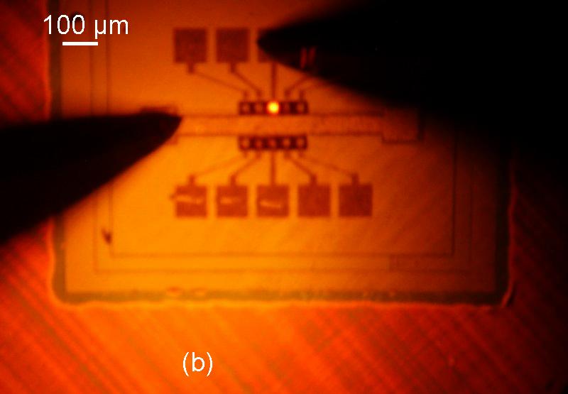

16 Monolithic Visible LED Arrays on Si using SOLES and CMOS-compatible processing Silicon On LatticeEngineered Silicon (SOLES) III-V Device Epi Silicon-like processing
 1.50E-007 1.")

17 P++ Si capped AlGaInP SDH LED on Ge and SiGe 2.50E-007 SEL231 SiGe 2.00E-007 Light Output (W) 1.50E E-007 Ge 200umx200um LED on Ge driven at 30mA 200umx200um LED on SiGe driven at 30mA 5.00E E Current (A) The higher thermal conductivity Of Silicon relative to Ge causes lower heating for LED on SiGe, increasing light power output


18 Compound Semiconductor Materials on Silicon (COSMOS) Compound Semiconductors on Silicon-on-Lattice-Engineered-Substrates (CS on SOLES)
19 Monolithic III-V-Si CMOS Systems COSMOS Integration of Si CMOS with InP HBTs Monolithic=Si industry and model Wide variety of products in single fab Leverage tools (software and hardware) Design platforms Level of abstraction allows a variety of products to be created at design-level Monolithic integration is previous solution to same problem historically ( tyranny of numbers ) Si
20 Summary III-V/Si not inhibited by previous fundamental issues Silicon-on-Lattice-Engineered-Silicon (SOLES) is a substrate embodiment easing the process integration of III-V+Si CMOS Demonstrated Part of COSMOS Visible optical devices on silicon 10 4 cm -2 threading dislocations on lattice constants matched to InGaP across visible spectrum Orange, yellow, and green semiconductor lasers could become a reality Concept of Si LED with embedded III-V active has been demonstrated on SOLES platform COSMOS program may be first step on path to real monolithic III- V-Si-CMOS circuits
Monolithic III-V/Si Integration
 Monolithic III-V/Si Integration The MIT Faculty has made this article openly available. Please share how this access benefits you. Your story matters. Citation As Published Publisher Fitzgerald, E.A. et
3.46 OPTICAL AND OPTOELECTRONIC MATERIALS
 Badgap Engineering: Precise Control of Emission Wavelength Wavelength Division Multiplexing Fiber Transmission Window Optical Amplification Spectrum Design and Fabrication of emitters and detectors Composition
Hybrid III-V/Si DFB laser integration on a 200 mm fully CMOS-compatible silicon photonics platform
 Hybrid III-V/Si DFB laser integration on a 200 mm fully CMOS-compatible silicon photonics platform B. Szelag 1, K. Hassan 1, L. Adelmini 1, E. Ghegin 1,2, Ph. Rodriguez 1, S. Bensalem 1, F. Nemouchi 1,
Chapter 3 Silicon Device Fabrication Technology
 Chapter 3 Silicon Device Fabrication Technology Over 10 15 transistors (or 100,000 for every person in the world) are manufactured every year. VLSI (Very Large Scale Integration) ULSI (Ultra Large Scale
Development of High-concentration Photovoltaics at Fraunhofer ISE: Cells and Systems
 Development of High-concentration Photovoltaics at Fraunhofer ISE: Cells and Systems Gerhard Peharz Fraunhofer-Institut für Solare Energiesysteme ISE 23 rd October 2008 Outline The Fraunhofer ISE III-V
200mm Next Generation MEMS Technology update. Florent Ducrot
 200mm Next Generation MEMS Technology update Florent Ducrot The Most Exciting Industries on Earth Semiconductor Display Solar 20,000,000x reduction in COST PER TRANSISTOR in 30 years 1 20x reduction in
Direct growth of III-V quantum dot materials on silicon
 Direct growth of III-V quantum dot materials on silicon John Bowers, Alan Liu, Art Gossard Director, Institute for Energy Efficiency University of California, Santa Barbara http://optoelectronics.ece.ucsb.edu/
Red InGaP light-emitting diodes epitaxially grown on engineered Ge-on-Si substrates
 Red InGaP light-emitting diodes epitaxially grown on engineered Ge-on-Si substrates The MIT Faculty has made this article openly available. Please share how this access benefits you. Your story matters.
Lect. 2: Basics of Si Technology
 Unit processes Thin Film Deposition Etching Ion Implantation Photolithography Chemical Mechanical Polishing 1. Thin Film Deposition Layer of materials ranging from fractions of nanometer to several micro-meters
EE 330 Lecture 9. IC Fabrication Technology Part II. -Oxidation -Epitaxy -Polysilicon -Planarization -Resistance and Capacitance in Interconnects
 EE 330 Lecture 9 IC Fabrication Technology Part II -Oxidation -Epitaxy -Polysilicon -Planarization -Resistance and Capacitance in Interconnects Review from Last Time Etching Dry etch (anisotropic) SiO
Non-Lattice Matched III-V Heterostructures for Ultrahigh Efficiency PV
 Non-Lattice Matched III-V Heterostructures for Ultrahigh Efficiency PV Harry Atwater 1, James Zahler 2, Melissa Griggs 1, Anna F. I. Morral 2, Sean Olson 2, Katsuaki Tanabe 1 1. California Institute of
Alternate Channel Materials for High Mobility CMOS
 Alternate Channel Materials for High Mobility CMOS By Christopher Henderson This year s International Electron Device Meeting (IEDM) discussed a wide range of approaches for creating CMOS transistors with
EECS130 Integrated Circuit Devices
 EECS130 Integrated Circuit Devices Professor Ali Javey 9/13/2007 Fabrication Technology Lecture 1 Silicon Device Fabrication Technology Over 10 15 transistors (or 100,000 for every person in the world)
Review of CMOS Processing Technology
 - Scaling and Integration Moore s Law Unit processes Thin Film Deposition Etching Ion Implantation Photolithography Chemical Mechanical Polishing 1. Thin Film Deposition Layer of materials ranging from
PHYS 534 (Fall 2008) Process Integration OUTLINE. Examples of PROCESS FLOW SEQUENCES. >Surface-Micromachined Beam
 Process Integration OUTLINE. Examples of PROCESS FLOW SEQUENCES. >Surface-Micromachined Beam") PHYS 534 (Fall 2008) Process Integration Srikar Vengallatore, McGill University 1 OUTLINE Examples of PROCESS FLOW SEQUENCES >Semiconductor diode >Surface-Micromachined Beam Critical Issues in Process
PHYS 534 (Fall 2008) Process Integration Srikar Vengallatore, McGill University 1 OUTLINE Examples of PROCESS FLOW SEQUENCES >Semiconductor diode >Surface-Micromachined Beam Critical Issues in Process
Figure 2.3 (cont., p. 60) (e) Block diagram of Pentium 4 processor with 42 million transistors (2000). [Courtesy Intel Corporation.
 (e) Block diagram of Pentium 4 processor with 42 million transistors (2000). [Courtesy Intel Corporation.") Figure 2.1 (p. 58) Basic fabrication steps in the silicon planar process: (a) oxide formation, (b) selective oxide removal, (c) deposition of dopant atoms on wafer, (d) diffusion of dopant atoms into exposed
Figure 2.1 (p. 58) Basic fabrication steps in the silicon planar process: (a) oxide formation, (b) selective oxide removal, (c) deposition of dopant atoms on wafer, (d) diffusion of dopant atoms into exposed
Instructor: Dr. M. Razaghi. Silicon Oxidation
 SILICON OXIDATION Silicon Oxidation Many different kinds of thin films are used to fabricate discrete devices and integrated circuits. Including: Thermal oxides Dielectric layers Polycrystalline silicon
Fabrication of high power GaN transistors F. Medjdoub CNRS - IEMN
 Fabrication of high power GaN transistors F. Medjdoub CNRS - IEMN E. Dogmus, A. Linge, T. Defais, R. Kabouche, R. Pecheux, M. Zegaoui Lille city centre Where are we? National Network of Large Technological
EE 434 Lecture 9. IC Fabrication Technology
 EE 434 Lecture 9 IC Fabrication Technology Quiz 7 The layout of a film resistor with electrodes A and B is shown. If the sheet resistance of the film is 40 /, determine the resistance between nodes A and
Czochralski Crystal Growth
 Czochralski Crystal Growth Crystal Pulling Crystal Ingots Shaping and Polishing 300 mm wafer 1 2 Advantage of larger diameter wafers Wafer area larger Chip area larger 3 4 Large-Diameter Wafer Handling
TEPZZ 5 Z 6A_T EP A1 (19) (11) EP A1 (12) EUROPEAN PATENT APPLICATION. (43) Date of publication: Bulletin 2012/46
 (11) EP A1 (12) EUROPEAN PATENT APPLICATION. (43) Date of publication: Bulletin 2012/46") (19) (12) EUROPEAN PATENT APPLICATION TEPZZ 5 Z 6A_T (11) EP 2 523 026 A1 (43) Date of publication: 14.11.2012 Bulletin 2012/46 (21) Application number: 12167332.1 (51) Int Cl.: G02B 6/12 (2006.01) G02B
(19) (12) EUROPEAN PATENT APPLICATION TEPZZ 5 Z 6A_T (11) EP 2 523 026 A1 (43) Date of publication: 14.11.2012 Bulletin 2012/46 (21) Application number: 12167332.1 (51) Int Cl.: G02B 6/12 (2006.01) G02B
5.8 Diaphragm Uniaxial Optical Accelerometer
 5.8 Diaphragm Uniaxial Optical Accelerometer Optical accelerometers are based on the BESOI (Bond and Etch back Silicon On Insulator) wafers, supplied by Shin-Etsu with (100) orientation, 4 diameter and
Microstructure of Electronic Materials. Amorphous materials. Single-Crystal Material. Professor N Cheung, U.C. Berkeley
 Microstructure of Electronic Materials Amorphous materials Single-Crystal Material 1 The Si Atom The Si Crystal diamond structure High-performance semiconductor devices require defect-free crystals 2 Crystallographic
ECSE 6300 IC Fabrication Laboratory Lecture 8 Metallization. Die Image
 ECSE 6300 IC Fabrication Laboratory Lecture 8 Metallization Prof. Rensselaer Polytechnic Institute Troy, NY 12180 Office: CII-6229 Tel.: (518) 276-2909 e-mails: luj@rpi.edu http://www.ecse.rpi.edu/courses/s18/ecse
IC Fabrication Technology Part III Devices in Semiconductor Processes
 EE 330 Lecture 10 IC Fabrication Technology Part III Metalization and Interconnects Parasitic Capacitances Back-end Processes Devices in Semiconductor Processes Resistors Diodes Review from Last Lecture
Silver Diffusion Bonding and Layer Transfer of Lithium Niobate to Silicon
 Chapter 5 Silver Diffusion Bonding and Layer Transfer of Lithium Niobate to Silicon 5.1 Introduction In this chapter, we discuss a method of metallic bonding between two deposited silver layers. A diffusion
Isolation Technology. Dr. Lynn Fuller
 ROCHESTER INSTITUTE OF TECHNOLOGY MICROELECTRONIC ENGINEERING Isolation Technology Dr. Lynn Fuller Motorola Professor 82 Lomb Memorial Drive Rochester, NY 14623-5604 Tel (585) 475-2035 Fax (585) 475-5041
Bulk crystal growth. A reduction in Lg will increase g m and f oper but with some costs
 Bulk crystal growth The progress of solid state device technology has depended not only on the development of device concepts but also on the improvement of materials. A reduction in Lg will increase g
Examples of dry etching and plasma deposition at Glasgow University
 Examples of dry etching and plasma deposition at Glasgow University Glasgow has pioneered and established many novel research activities involving the development of new dry etch processes and dry etch
EE 330 Lecture 9. IC Fabrication Technology Part 2
 EE 330 Lecture 9 IC Fabrication Technology Part 2 Quiz 8 A 2m silicon crystal is cut into wafers using a wire saw. If the wire diameter is 220um and the wafer thickness is 350um, how many wafers will this
Silicon-on-insulator (SOI) was developed in the
 was developed in the") 66 Silicon-on-insulator substrates for compound semiconductor applications Mike Cooke reports on research developments reaching towards high-power electronics and infrared optical communications. Silicon-on-insulator
66 Silicon-on-insulator substrates for compound semiconductor applications Mike Cooke reports on research developments reaching towards high-power electronics and infrared optical communications. Silicon-on-insulator
SiGeC Cantilever Micro Cooler
 Mat. Res. Soc. Symp. Proc. Vol. 793 2004 Materials Research Society S11.3.1 SiGeC Cantilever Micro Cooler Gehong Zeng, Ali Shakouri 1 *, Edward Croke 2, Yan Zhang 1, James Christofferson 1 and John E.
Microelettronica. Planar Technology for Silicon Integrated Circuits Fabrication. 26/02/2017 A. Neviani - Microelettronica
 Microelettronica Planar Technology for Silicon Integrated Circuits Fabrication 26/02/2017 A. Neviani - Microelettronica Introduction Simplified crosssection of an nmosfet and a pmosfet Simplified crosssection
EE 330 Lecture 9. IC Fabrication Technology Part II. -Oxidation -Epitaxy -Polysilicon -Planarization -Resistance and Capacitance in Interconnects
 EE 330 Lecture 9 IC Fabrication Technology Part II -Oxidation -Epitaxy -Polysilicon -Planarization -Resistance and Capacitance in Interconnects Review from Last Time IC Fabrication Technology Crystal Preparation
Molecular Beam Deposition of Low-Resistance Polycrystalline InAs
 Molecular Beam Deposition of Low-Resistance Polycrystalline InAs D. Scott, M. Urteaga, N. Parthasarathy, J.H. English and M.J.W. Rodwell Department of Electrical and Computer Engineering University of
Chapter 2 Manufacturing Process
 Digital Integrated Circuits A Design Perspective Chapter 2 Manufacturing Process 1 CMOS Process 2 CMOS Process (n-well) Both NMOS and PMOS must be built in the same silicon material. PMOS in n-well NMOS
A discussion of crystal growth, lithography, etching, doping, and device structures is presented in
 Chapter 5 PROCESSING OF DEVICES A discussion of crystal growth, lithography, etching, doping, and device structures is presented in the following overview gures. SEMICONDUCTOR DEVICE PROCESSING: AN OVERVIEW
The integration of InGaP LEDs with CMOS on 200 mm silicon wafers
 The integration of InGaP LEDs with CMOS on 200 mm silicon wafers The MIT Faculty has made this article openly available. Please share how this access benefits you. Your story matters. Citation As Published
Chapter 4. UEEP2613 Microelectronic Fabrication. Oxidation
 Chapter 4 UEEP2613 Microelectronic Fabrication Oxidation Prepared by Dr. Lim Soo King 24 Jun 2012 Chapter 4...113 Oxidation...113 4.0 Introduction... 113 4.1 Chemistry of Silicon Dioxide Formation... 115
MICROCHIP MANUFACTURING by S. Wolf
 MICROCHIP MANUFACTURING by S. Wolf Chapter 7: BASICS OF THIN FILMS 2004 by LATTICE PRESS Chapter 7: Basics of Thin Films CHAPTER CONTENTS Terminology of Thin Films Methods of Thin-Film Formation Stages
Impurity free vacancy disordering of InGaAs quantum dots
 JOURNAL OF APPLIED PHYSICS VOLUME 96, NUMBER 12 15 DECEMBER 2004 Impurity free vacancy disordering of InGaAs quantum dots P. Lever, H. H. Tan, and C. Jagadish Department of Electronic Materials Engineering,
New Applications of CMP for Non-Traditional Semiconductor Manufacturing. Robert L. Rhoades, Ph.D. Entrepix, Inc.
 New Applications of CMP for Non-Traditional Semiconductor Manufacturing Robert L. Rhoades, Ph.D. Entrepix, Inc. Outline Introduction New Applications of CMP MEMS Non-CMOS Devices New Materials Epitaxial
Isolation of elements
 1 In an IC, devices on the same substrate must be isolated from one another so that there is no current conduction between them. Isolation uses either the junction or dielectric technique or a combination
EE 330 Lecture 8. IC Fabrication Technology Part II. - Oxidation - Epitaxy - Polysilicon - Interconnects
 EE 330 Lecture 8 IC Fabrication Technology Part II - Oxidation - Epitaxy - Polysilicon - Interconnects Review from Last Time MOS Transistor Bulk Source Gate Drain p-channel MOSFET Lightly-doped n-type
Lecture 22: Integrated circuit fabrication
 Lecture 22: Integrated circuit fabrication Contents 1 Introduction 1 2 Layering 4 3 Patterning 7 4 Doping 8 4.1 Thermal diffusion......................... 10 4.2 Ion implantation.........................
Compact hybrid plasmonic-si waveguide structures utilizing Albanova E-beam lithography system
 Compact hybrid plasmonic-si waveguide structures utilizing Albanova E-beam lithography system Introduction Xu Sun Laboratory of Photonics and Microwave Engineering, Royal Institute of Technology (KTH),
HOMEWORK 4 and 5. March 15, Homework is due on Monday March 30, 2009 in Class. Answer the following questions from the Course Textbook:
 HOMEWORK 4 and 5 March 15, 2009 Homework is due on Monday March 30, 2009 in Class. Chapter 7 Answer the following questions from the Course Textbook: 7.2, 7.3, 7.4, 7.5, 7.6*, 7.7, 7.9*, 7.10*, 7.16, 7.17*,
Strained Silicon-On-Insulator Fabrication and Characterization
 10.1149/1.2728880, The Electrochemical Society Strained Silicon-On-Insulator Fabrication and Characterization M. Reiche a, C. Himcinschi a, U. Gösele a, S. Christiansen a, S. Mantl b, D. Buca b, Q.T. Zhao
Germanium and silicon photonics
 76 Technical focus: III-Vs on silicon optoelectronics Germanium and silicon photonics Mike Cooke reports on recent research using germanium to enable infrared light-emitting devices to be created on silicon
SKW Wafer Product List
 SKW Wafer Product List Regularly updated (2.13.2018) SKW Associates, INC. 2920 Scott Blvd, Santa Clara, CA 95054 Tel: 408-919-0094, Fax: 408-919-0097 I. Available Wafers in 200mm and 300mm - Please refer
PROCESS FLOW AN INSIGHT INTO CMOS FABRICATION PROCESS
 Contents: VI Sem ECE 06EC63: Analog and Mixed Mode VLSI Design PROCESS FLOW AN INSIGHT INTO CMOS FABRICATION PROCESS 1. Introduction 2. CMOS Fabrication 3. Simplified View of Fabrication Process 3.1 Alternative
Advanced Gate Stack, Source/Drain, and Channel Engineering for Si-Based CMOS 6: New Materials, Processes, and Equipment
 Advanced Gate Stack, Source/Drain, and Channel Engineering for Si-Based CMOS 6: New Materials, Processes, and Equipment Editors: E. P. Gusev Qualcomm MEMS Technologies San Jose, California, USA D-L. Kwong
Transmission Mode Photocathodes Covering the Spectral Range
 Transmission Mode Photocathodes Covering the Spectral Range 6/19/2002 New Developments in Photodetection 3 rd Beaune Conference June 17-21, 2002 Arlynn Smith, Keith Passmore, Roger Sillmon, Rudy Benz ITT
Materials Characterization
 Materials Characterization C. R. Abernathy, B. Gila, K. Jones Cathodoluminescence (CL) system FEI Nova NanoSEM (FEG source) with: EDAX Apollo silicon drift detector (TE cooled) Gatan MonoCL3+ FEI SEM arrived
Metallization. Typical current density ~10 5 A/cm 2 Wires introduce parasitic resistance and capacitance
 Metallization Interconnects Typical current density ~10 5 A/cm 2 Wires introduce parasitic resistance and capacitance RC time delay Inter-Metal Dielectric -Prefer low dielectric constant to reduce capacitance
Crystalline Silicon Solar Cells
 12 Crystalline Silicon Solar Cells As we already discussed in Chapter 6, most semiconductor materials have a crystalline lattice structure. As a starting point for our discussion on crystalline silicon
Microelectronics. Integrated circuits. Introduction to the IC technology M.Rencz 11 September, Expected decrease in line width
 Microelectronics Introduction to the IC technology M.Rencz 11 September, 2002 9/16/02 1/37 Integrated circuits Development is controlled by the roadmaps. Self-fulfilling predictions for the tendencies
id : class06 passwd: class06
 http://wwwee.stanford.edu/class_directory.php http://ocw.mit.edu/ocwweb/index.htm http://nanosioe.ee.ntu.edu.tw id : class06 passwd: class06 Display and OLED Market OLED on glass only ~US$ 0.5B in 04,
SEMATECH Symposium Korea 2012 Practical Analysis Techniques of Nanostructured Semiconductors by Electron Microscopy
 SEMATECH Symposium Korea 2012 Practical Analysis Techniques of Nanostructured Semiconductors by Electron Microscopy Jun-Mo Yang, Ph.D. Measurement & Analysis Team National NanoFab Center, Korea Introduction
A Novel Low Temperature Self-Aligned Field Induced Drain Polycrystalline Silicon Thin Film Transistor by Using Selective Side-Etching Process
 Chapter 3 A Novel Low Temperature Self-Aligned Field Induced Drain Polycrystalline Silicon Thin Film Transistor by Using Selective Side-Etching Process 3.1 Introduction Low-temperature poly-si (LTPS) TFTs
EE 143 CMOS Process Flow
 EE 143 CMOS rocess Flow CT 84 D D G Sub G Sub S S G D S G D S + + + + - MOS Substrate Well - MOS Substrate EE 143 CMOS rocess Flow CT 85 hotoresist Si 3 4 SiO 2 Substrate selection: moderately high resistivity,
Method to obtain TEOS PECVD Silicon Oxide Thick Layers for Optoelectronics devices Application
 Method to obtain TEOS PECVD Silicon Oxide Thick Layers for Optoelectronics devices Application ABSTRACT D. A. P. Bulla and N. I. Morimoto Laboratório de Sistemas Integráveis da EPUSP São Paulo - S.P. -
Chapter 6. AlGaAs/GaAs/GaAs Wafer-fused HBTs
 Chapter 6. AlGaAs/GaAs/GaAs Wafer-fused HBTs 6.1. Overview Previous chapters described an AlGaAs-GaAs-GaN HBT, in which an epitaxially grown AlGaAs-GaAs emitter-base was wafer-fused to a GaN collector.
Exam 1 Friday Sept 22
 Exam 1 Friday Sept 22 Students may bring 1 page of notes Next weeks HW assignment due on Wed Sept 20 at beginning of class No 5:00 p.m extension so solutions can be posted Those with special accommodation
Complementary Metal Oxide Semiconductor (CMOS)
") Technische Universität Graz Institute of Solid State Physics Complementary Metal Oxide Semiconductor (CMOS) Franssila: Chapters 26,28 Technische Universität Graz Institute of Solid State Physics Complementary
Technische Universität Graz Institute of Solid State Physics Complementary Metal Oxide Semiconductor (CMOS) Franssila: Chapters 26,28 Technische Universität Graz Institute of Solid State Physics Complementary
Applications. SIMS successfully applied to many fields. Catalysts, metals, ceramics, minerals may primarily use imaging
 Applications SIMS successfully applied to many fields Catalysts, metals, ceramics, minerals may primarily use imaging Semiconductors extensively use depth profiling Si, GaAs, GaN, ZnO Minerals Analysis
9/4/2008 GMU, ECE 680 Physical VLSI Design
 ECE680: Physical VLSI Design Chapter II CMOS Manufacturing Process 1 Dual-Well Trench-Isolated CMOS Process gate-oxide TiSi 2 AlCu Tungsten SiO 2 p-well poly n-well SiO 2 n+ p-epi p+ p+ 2 Schematic Layout
Current Gain Dependence on Subcollector and Etch-Stop Doping in InGaP/GaAs HBTs
 IEEE TRANSACTIONS ON ELECTRON DEVICES, VOL. 48, NO. 5, MAY 2001 835 Current Gain Dependence on Subcollector and Etch-Stop Doping in InGaP/GaAs HBTs Theodore Chung, Seth R. Bank, John Epple, and Kuang-Chien
Stanford University. MOCVD growth of III-V & III-N nanostructures, thin films and heterostructures
 MOCVD growth of III-V & III-N nanostructures, thin films and heterostructures Outline 1 2 3 MOCVD introduction MOCVD capability in SNF Work done in MOCVD lab 1. Nanostructures Catalyst free periodic nanoarrays
Ultra Low Resistance Ohmic Contacts to InGaAs/InP
 Ultra Low Resistance Ohmic Contacts to InGaAs/InP Uttam Singisetti*, A.M. Crook, E. Lind, J.D. Zimmerman, M. A. Wistey, M.J.W. Rodwell, and A.C. Gossard ECE and Materials Departments University of California,
IC/MEMS Fabrication - Outline. Fabrication
 IC/MEMS Fabrication - Outline Fabrication overview Materials Wafer fabrication The Cycle: Deposition Lithography Etching Fabrication IC Fabrication Deposition Spin Casting PVD physical vapor deposition
Copper Interconnect Technology
 Tapan Gupta Copper Interconnect Technology i Springer Contents 1 Introduction 1 1.1 Trends and Challenges 2 1.2 Physical Limits and Search for New Materials 5 1.3 Challenges 6 1.4 Choice of Materials 7
Aqueous Ammonium Sulfide Passivation and Si 1-x Ge x MOSCaps
 Aqueous Ammonium Sulfide Passivation and Si 1-x Ge x MOSCaps Lauren Peckler 1, Stacy Heslop 2, and Anthony Muscat 1 1 Department of Chemical & Environmental Engineering, University of Arizona 2 Department
EE 330 Lecture 8. IC Fabrication Technology Part II. - Masking - Photolithography - Deposition - Etching - Diffusion
 EE 330 Lecture 8 IC Fabrication Technology Part II?? - Masking - Photolithography - Deposition - Etching - Diffusion Review from Last Time Technology Files Provide Information About Process Process Flow
Surface Micromachining
 Surface Micromachining Micro Actuators, Sensors, Systems Group University of Illinois at Urbana-Champaign Outline Definition of surface micromachining Most common surface micromachining materials - polysilicon
Cu CMP: Macro-scale Manufacturing for Nano-scale Quality Requirements
 Cu CMP: Macro-scale Manufacturing for Nano-scale Quality Requirements Jung-Hoon Chun Laboratory for Manufacturing and Productivity Massachusetts Institute of Technology Cambridge, MA 02139 April 23, 2009
2-1 Introduction The demand for high-density, low-cost, low-power consumption,
 Chapter 2 Hafnium Silicate (HfSi x O y ) Nanocrystal SONOS-Type Flash Memory Fabricated by Sol-Gel Spin Coating Method Using HfCl 4 and SiCl 4 as Precursors 2-1 Introduction The demand for high-density,
Micro-Electro-Mechanical Systems (MEMS) Fabrication. Special Process Modules for MEMS. Principle of Sensing and Actuation
 Fabrication. Special Process Modules for MEMS. Principle of Sensing and Actuation") Micro-Electro-Mechanical Systems (MEMS) Fabrication Fabrication Considerations Stress-Strain, Thin-film Stress, Stiction Special Process Modules for MEMS Bonding, Cavity Sealing, Deep RIE, Spatial forming
Micro-Electro-Mechanical Systems (MEMS) Fabrication Fabrication Considerations Stress-Strain, Thin-film Stress, Stiction Special Process Modules for MEMS Bonding, Cavity Sealing, Deep RIE, Spatial forming
Oxidation Part 1. By Christopher Henderson
 Oxidation Part 1 By Christopher Henderson In this new series, we will discuss the subject of oxidation. Oxidation is a key aspect of the semiconductor process. The fact that one can easily grow an oxide
Motorola PC603R Microprocessor
 Construction Analysis Motorola PC603R Microprocessor Report Number: SCA 9709-551 Global Semiconductor Industry the Serving Since 1964 17350 N. Hartford Drive Scottsdale, AZ 85255 Phone: 602-515-9780 Fax:
Epitaxial Growth of Low Defect SiGe Buffer Layers for Integration of New Materials on 300 mm Silicon Wafers. Semicon Europa 2017
 Layers for Integration of New Materials on 300 mm Silicon Wafers Peter Storck Semicon Europa 2017 Integration of new Materials is Part of the Logic Roadmap CMOS logic evolves from planar to FinFET and
CMOS Technology. Flow varies with process types & company. Start with substrate selection. N-Well CMOS Twin-Well CMOS STI
 CMOS Technology Flow varies with process types & company N-Well CMOS Twin-Well CMOS STI Start with substrate selection Type: n or p Doping level, resistivity Orientation, 100, or 101, etc Other parameters
1 HRL Laboratories, LLC, Malibu, California, Baskin School of Engineering, University of California, Santa Cruz, CA *
 High Cooling Power Density of SiGe/Si Superlattice Microcoolers Gehong Zeng, Xiaofeng Fan, Chris LaBounty, John E. Bowers, Edward Croke, James Christofferson, Daryoosh Vashaee, Yan Zhang, and Ali Shakouri
Lecture 7 CMOS MEMS. CMOS MEMS Processes. CMOS MEMS Processes. Why CMOS-MEMS? Agenda: CMOS MEMS: Fabrication. MEMS structures can be made
 EEL6935 Advanced MEMS (Spring 2005) Instructor: Dr. Huikai Xie CMOS MEMS Agenda: Lecture 7 CMOS MEMS: Fabrication Pre-CMOS Intra-CMOS Post-CMOS Deposition Etching Why CMOS-MEMS? Smart on-chip CMOS circuitry
Lecture Day 2 Deposition
 Deposition Lecture Day 2 Deposition PVD - Physical Vapor Deposition E-beam Evaporation Thermal Evaporation (wire feed vs boat) Sputtering CVD - Chemical Vapor Deposition PECVD LPCVD MVD ALD MBE Plating
VLSI INTRODUCTION P.VIDYA SAGAR ( ASSOCIATE PROFESSOR) Department of Electronics and Communication Engineering, VBIT
 Department of Electronics and Communication Engineering, VBIT") VLSI INTRODUCTION P.VIDYA SAGAR ( ASSOCIATE PROFESSOR) contents UNIT I INTRODUCTION: Introduction to IC Technology MOS, PMOS, NMOS, CMOS & BiCMOS technologies. BASIC ELECTRICAL PROPERTIES : Basic Electrical
VLSI INTRODUCTION P.VIDYA SAGAR ( ASSOCIATE PROFESSOR) contents UNIT I INTRODUCTION: Introduction to IC Technology MOS, PMOS, NMOS, CMOS & BiCMOS technologies. BASIC ELECTRICAL PROPERTIES : Basic Electrical
Epitaxial MoSe 2 semiconductor heterostructures on AlN/Si(111) substrates A. Dimoulas, NCSR DEMOKRITOS
 substrates A. Dimoulas, NCSR DEMOKRITOS") Epitaxial MoSe 2 semiconductor heterostructures on AlN/Si(111) substrates A. Dimoulas, NCSR DEMOKRITOS Acknowledgements NCSR DEMOKRITOS, Greece E. Xenogiannopoulou, P. Tsipas, D. Tsoutsou, K. Aretouli,
Epitaxial MoSe 2 semiconductor heterostructures on AlN/Si(111) substrates A. Dimoulas, NCSR DEMOKRITOS Acknowledgements NCSR DEMOKRITOS, Greece E. Xenogiannopoulou, P. Tsipas, D. Tsoutsou, K. Aretouli,
Latching Shape Memory Alloy Microactuator
 Latching Shape Memory Alloy Microactuator ENMA490, Fall 00 S. Cabrera, N. Harrison, D. Lunking, R. Tang, C. Ziegler, T. Valentine Outline Background Problem Project Development Design Evaluation Applications
Low D it High-k/In 0.53 Ga 0.47 As Gate Stack with CET down to 0.73 nm and Thermally Stable Silicide Contact by Suppression of Interfacial Reaction
 IEDM 2013 Dec 9 th, 2013 Low D it High-k/In 0.53 Ga 0.47 As Gate Stack with CET down to 0.73 nm and Thermally Stable Silicide Contact by Suppression of Interfacial Reaction D. Hassan Zadeh, H. Oomine,
Semiconductor Optical Communication Components and Devices Lecture 8: Epitaxial growth - I (Techniques)
") Semiconductor Optical Communication Components and Devices Lecture 8: Epitaxial growth - I (Techniques) Prof. Utpal Das Professor, Department of Electrical Engineering, Laser Technology Program, Indian
Semiconductor Optical Communication Components and Devices Lecture 8: Epitaxial growth - I (Techniques) Prof. Utpal Das Professor, Department of Electrical Engineering, Laser Technology Program, Indian
1 MARCH 2017 FILM DEPOSITION NANOTECHNOLOGY
 1 MARCH 2017 FILM DEPOSITION NANOTECHNOLOGY PRESENTATION Pedro C. Feijoo E-mail: PedroCarlos.Feijoo@uab.cat FABRICATION TECHNOLOGIES FOR NANOELECTRONIC DEVICES. PEDRO C. FEIJOO 2 FILM GROWTH Chemical vapor
Radiation Tolerant Isolation Technology
 Radiation Tolerant Isolation Technology Background The following contains a brief description of isolation technologies used for radiation hardened integrated circuits. The technologies mentioned are junction
GROWTH AND INVESTIGATION OF INDIUM ARSENIDE BASED DIODE HETEROSTRUCTURES FOR MID INFRARED APPLICATION
 GROWTH AND INVESTIGATION OF INDIUM ARSENIDE BASED DIODE HETEROSTRUCTURES FOR MID INFRARED APPLICATION V.A. Gevorkyan, K.M. Gambaryan, and M.S. Kazaryan Yerevan State University, E-mail: vgev@ysu.am 1.
Chapter 3 CMOS processing technology
 Chapter 3 CMOS processing technology (How to make a CMOS?) Si + impurity acceptors(p-type) donors (n-type) p-type + n-type => pn junction (I-V) 3.1.1 (Wafer) Wafer = A disk of silicon (0.25 mm - 1 mm thick),
Passivation of InAs and GaSb with novel high dielectrics
 Passivation of InAs and GaSb with novel high dielectrics Professor Minghwei HONG Department of Materials Science and Engineering, National Tsing Hua University 101, Section 2, Kuang-Fu Rd., Hsinchu, Taiwan,
Lecture 19 Microfabrication 4/1/03 Prof. Andy Neureuther
 EECS 40 Spring 2003 Lecture 19 Microfabrication 4/1/03 Prof. ndy Neureuther How are Integrated Circuits made? Silicon wafers Oxide formation by growth or deposition Other films Pattern transfer by lithography
Metallization. Typical current density ~105 A/cm2 Wires introduce parasitic resistance and capacitance
 Metallization Interconnects Typical current density ~105 A/cm2 Wires introduce parasitic resistance and capacitance RC time delay Inter-Metal Dielectric -Prefer low dielectric constant to reduce capacitance
Low Temperature Dielectric Deposition for Via-Reveal Passivation.
 EMPC 2013, September 9-12, Grenoble; France Low Temperature Dielectric Deposition for Via-Reveal Passivation. Kath Crook, Mark Carruthers, Daniel Archard, Steve Burgess, Keith Buchanan SPTS Technologies,
Chapter 5 Thermal Processes
 Chapter 5 Thermal Processes 1 Topics Introduction Hardware Oxidation Diffusion Annealing Post-Implantation Alloying Reflow High Temp CVD Epi Poly Silicon Nitride RTP RTA RTP Future Trends 2 Definition
Interconnects. Outline. Interconnect scaling issues Aluminum technology Copper technology. Properties of Interconnect Materials
 Interconnects Outline Interconnect scaling issues Aluminum technology Copper technology 1 Properties of Interconnect Materials Metals Silicides Barriers Material Thin film Melting resistivity point ( C)