Bulk Silicon Micromachining
|
|
|
- Jane Cook
- 6 years ago
- Views:
Transcription

1 Bulk Silicon Micromachining Micro Actuators, Sensors, Systems Group University of Illinois at Urbana-Champaign
2 Outline Types of bulk micromachining silicon anisotropic etching crystal orientation isotropic etching of liquid and gas phase etchants Silicon anisotropic etching influence on etch rate by orientation influence on etch rate by doping concentration Etching simulation with ACES
3 Definition Silicon bulk micromachining processes that involve partial removal of bulk material in order to create three dimensional structures or free devices. General micromachining machining process that involves removal of substrate materials in order to render functional devices.
4 Example of a Bulk Etching Schematic diagram of the process for a pressure sensor.

5 Example of Bulk Etching Micromachined AFM/STM probe

6 Example of Bulk Machining Stanford University Neuron Probe Development of complete analog signal processing electronics package. Demonstration of successful, repeated recordings from rat cerebellar cortex and tissues slices with multi-channel data acquisition. A combination of plasma etching and selective wet etch stopping is used to define the overall shape of the probes. Multi-level metallization with thin-film iridium microelectrode sites allows for small and constant probe cross section.


7 Micromachined Neuron Wells In order to really get at the dynamics of a functioning neuronal network, you need to know what all the different components are doing at the same time. To study plasticity, where interconnections between the neurons change based on the activity patterns, you need to be able to influence the cells without damaging them. To study development, where the various pieces of the network are changing, you also need to be able to measure the activities of the same neurons over time. Otherwise you're stuck making statistical analyses of the activities, which is far less helpful.

8 Stanford Thermal RMS Converter Using a standard CMOS process, n-wells are biased so that they self-passivate while selectively exposed p-silicon (substrate) is etched, resulting in single-crystal silicon islands that are suspended above etched pits by oxide/aluminum members. This approach allows for thermal isolation of entire active circuits or any subset of them, based on components that can be fabricated in an n-well. Demonstration of very highly thermally isolated (60,000 degrees/watt) single-crystal silicon islands. Demonstration of thermally-stabilized band-gap voltage reference. Demonstration of >400 MHz, 60 db dynamic range thermal RMS converter with on-chip CMOS servo circuits. Demonstration of digitally controlled, fully integrated thermal (Pirani-type) vacuum sensor.
 active tactile sensor array.")
9 Goals Example of Bulk Micromachining Micro tactile sensor Development of a CMOS-compatible tactile sensor with independent x- and y-axis shear and normal force sensing capability. Integration of all necessary multiplexing and power switching circuitry onto a single chip to enable a large (approximately 2 X 2 cm) active tactile sensor array. Technical Approach: Composite (silicon dioxide/polysilicon/silicon dioxide/aluminum/silicon nitride sandwitch) plates suspended by four bridges with embedded strain sensing polysilicon piezoresistors. Shuttle plate is allowed to translate by an undercut etch of the underlying bulk silicon by with a wet a tetramethyl ammonium hydroxide (TMAH) etch. By algebraically combining the output signals from the four strain gauges, independent measures of x- and y-axis shear and normal forces is available. The fabrication process used is fully CMOS compatible.
10 Anisotropic Etching Etching rate is dependant on the crystal orientation. The difference in etch rate is used creatively to generate unique 3D structures. undercut anisotropic depth depth isotropic

11 Silicon <110> View
12 Silicon Wafer Orientation
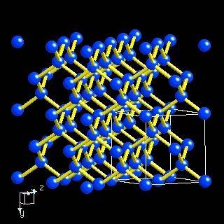
13 Lattice Forest Wafer Orientation {100} {100} {110} {111} 3D Lattice and top z y x y z x y z x y z x surface Lattice top view z y x z y x z y x z y x
14 Example

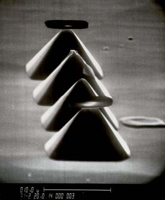
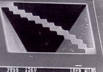
15 A silicon Cavity
16 Telling Wafer Orientation by Flats
17 Crystal Orientation - Miller Index The orientation of a surface or a crystal plane may be defined by considering how the plane (or indeed any parallel plane) intersects the main crystallographic axes of the solid. The application of a set of rules leads to the assignment of the Miller Indices, (hkl) ; a set of numbers which quantify the intercepts and thus may be used to uniquely identify the plane or surface. The following treatment of the procedure used to assign the Miller Indices is a simplified one (it may be best if you simply regard it as a "recipe") and only a cubic crystal system (one having a cubic unit cell with dimensions a x a x a ) will be considered.
18 Construction of Miller Index The procedure is most easily illustrated using an example so we will first consider the following surface/plane: Step 1 : Identify the intercepts on the x-, y- and z- axes. In this case the intercept on the x-axis is at x = a ( at the point (a,0,0) ), but the surface is parallel to the y- and z-axes - strictly therefore there is no intercept on these two axes but we shall consider the intercept to be at infinity ( ) for the special case where the plane is parallel to an axis. The intercepts on the x-, y- and z-axes are thus Intercepts : a,,
19 Construction of Miller Index Step 2 : Specify the intercepts in fractional co-ordinates Take the reciprocals of the three integers found in Step 1 and reduce them to the smallest set of integers h, k and l. Fractional Intercepts : a/a, /α, /α ι.ε. 1,, Miller Indices : (100) So the surface/plane illustrated is the (100) plane of the cubic crystal. Check 340 text book for more details; or chapter 2 of binder notes.
20 Construction of Miller Index Equivalent planes Three equivalent planes (100), (010) and (001) belong to the {100} family. Notice the notification.
21 Miller Index Other low index planes.
22 High Index Plane Example {211} Plane
23 Etch Rate is A Function of Direction Etch of wagon-wheel pattern to reveal difference in etch rate is different wafer orientations. <111>

24 Etching System - Reflux system Hot plate Reflux system
25 Etch in Anisotropic Etchant The masked region is not etched. The slopped region {111} slows forms but etches slowly. The bottom surface {100} etches quickly (tens of micrometers per second).
26 Results after extended etching The vertical distance d is etch rate in <100> direction times the duration. The lateral distance t is [etch rate in <111> direction times the duration]/sin(54.75).
27 Idealized Case Zero lateral undercut. Almost always true as the etch rate ratio of <100> and <111> can reaches several hundred.
28 Commonly Used Silicon Etchants (Fig. 3, Chapter 8, Binder Handout) EDP (Ethylene diamine pyrocatechol) 90o (p. 43) sometimes refers to EPW, Ethylenediamine Pyrocatechol and Water) Etch rate ratio for <100> and <111> is as high as 35:1 or higher (Petersen paper, chpt. 1, Binder notes) Etch rate for silicon nitride and silicon oxide is almost negligible. Even native oxide (see next page) becomes important in processing Highly directional selective, allows cheap oxide as mask. Expensive; chemically unstable. Aging: etch rate and color changes with time after exposure to oxygen. KOH (Potassium hydroxide) 75-90o (* p. 36) various concentration can be used, wt % is common. Etch rate ratio for,100> and <111> is also very high (even higher than that of EDP). Etch rate on silicon nitride (LPCVD) is negligible. Etch rate on silicon oxide is not negligible. 14 angstrom/min. (thermally grown oxide quality). e.g. a process last for 10 hours consumes 0.84 µm of oxide. Other TMAH (tetramethyl ammonium hydroxide) (* 40)
29 Commonly Used Isotropic Etchant HNA Hydrofluoric acid + Nitric Acid + Acetic acid Various mixing ratios are possible, resulting in different etch rates. Because the solution contains HF, the etch rate on oxide is relatively quick, 300 Angstrom/min. * 32 text book. Room temperature process.
30 Etching Rules For convex corners, the fastest etching planes dominate the three-dimensional shape. For concave corners, the slowest etching planes dominate the three dimensional shape. <110> <110> <100>
31 Etch Profile Extended etching produces inverted pyramid by undercutting a convex structure (e.g. cantilever diving board beam in this case). Red lines illustration etching profile evolution with time under the convex structure. (* p. 34, 35)
32 Etch Profile
33 Perspective View of Etching Profile
34 Real-life Case Convex corners are removed at fast etch rates. See mask and simulation below.


35 More Complex Cases Inverted pyramid is the final stable shape. For an arbitrary shaped mask with transparent opening, the pyramidal shape is bound by the outside boundary. mask
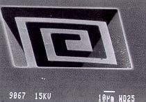
36 Etching Simulation Software As the mask shape becomes complex, it becomes more and more difficult to precisely predict the etching process and visualizing the results. Anisotropic Crystalline Etching Simulation (ACES) Software to the help. Demo copy of software can be found at
37 How does etchants remove silicon According to commonly accepted theory, the silicon etchants contain oxidation and reducing agents. The oxidation agents first turns silicon into silicon oxide the reducing agents then etches the oxide away.
38 Who Etches Who - A Key to Designing Any Micromachining Process A comprehensive etch rate table can be found in the following resources: paper titled etch rates for micromachining processing by K. Williams, JMEMS, Vol. 5, No. 4, p. 256, Paper titled silicon as a mechanical material by Kurt Petersen, Bind Notes, Chapter 1. Etch rate table, p. 30, * Kovacs text book. Other chemical and physical handbooks (e.g. CRC handbook). A comprehensive understanding of etch rate is built through experience and research in the MEMS field.
39 Native Oxide (* Chapter 2, 4.2) Oxide formed on silicon when a bare and clean silicon is exposed to atmosphere at room temperature typically tens of angstrom of oxide can be formed. How to determine whether native oxide has formed? Pure silicon surface is hydrophobic water will bead off. Oxide silicon surface becomes hydrophilic. Water will attach and spread.
40 If the diaphragm is made of silicon nitride; because the etch rate of EDP and KOH on nitride is negligible, it is possible to etch the silicon by directly immersing nitridecoated wafers in etchant. Nitride has tensile intrinsic stress. Thickness typically < 1.5 µm. Not good for large thickness because the time to grow LPCVD nitride will be excessively long. EDP or KOH etching are both possible. Forming a Silicon Diaphragm (I)
41 Forming a Silicon Diaphragm (I) To form a silicon membrane (e.g. thickness > 3-10 µm), timed etch is to be used. Use silicon oxide as the etching mask oxide can be removed easily using HF after the device is made. Use EDP or KOH to etch the materials if KOH is used, attention must be paid to the thickness of oxide. Calibrate the etch rate and the thickness of the wafer carefully.
42 Shortcomings of Timed Etch Etch rate varies with the age of the solution for Edp Etch rate is not uniform across the entire wafer area some regions may be under etched while others over etched. Etch rate can also vary as a function of temperature and concentration. Bottom line: timed etching must be used carefully and discriminatively in order to achieve efficiency in fabrication.
43 Etch Rate is a Function of the Doping Concentration Highly doped silicon exhibit much reduced etch rate compared with lowly doped silicon. in EDP, doping concentration greater than 7x10 19 cm -3 results in etch rate reduction of about 50; in KOH, doping greater than cm -3 decreases etch rate by 20. Doping concentration can be specified by diffusion doping ion implantation + annealing (drive in) wafer bonding
44 Forming Micro Diaphragm using Etch Stop Layer (* 46-47) Dope silicon with boron or phorphous to reach desired high doping concentration. Doping is associated with much better uniformity and repeatability. Use oxide as a mask for back-side etching etching automatically stops when the doped layer is reached.
45 Examples of Applications Scanning probe microscopes Neuron probes micromachined RF devices


46 Digital Instruments SPM Probe Based on Stanford Process Force (or Spring) Constants 0.58, 0.32, 0.12, 0.06 N/m * Nominal Tip Radius of Curvature 20-60nm Cantilever Lengths 100 & 200µm Cantilever Configuration V-shaped Reflective Coating Gold Shape of Tip Square Pyramidal
47 Silicon nitride serving as the cantilever beam material. Step 1: oxidation of silicon with front surface being {100}. Step 2: pattern oxidation surface to create an open square with edges aligned to <110>. Step 3: etching of silicon in EDP or KOH solutions (KOH is possible is depth is not big.) The width of the opening and the depth is related. t = tan(54.75 ) o w 2 Stanford SPM
48 Stanford SPM (Continued) Step 4: removal of oxide in HF, and deposit silicon nitride film (on both sides). Step 5: Pattern front side nitride and remove backside nitride using plasma etching. Step 6: bond a glass chip to the front side to serve as a handle. Step 7: Remove the entire bulk region to form the AFM/STM probe.
49 Relative Shortcomings of Stanford SPM Tip radius relatively limited due to etching shape (inverted pyramid) as the tip is formed by molded silicon nitride, the shape is determined by the inverted pyramid. The silicon nitride stress is not repeatable and could result in non-uniform performance.
50 All Silicon SPM Probe Probe made of single-crystal silicon and thus has zero intrinsic stress. The tip is made of silicon such that it could be sharpened after the process is completed.
51 All Silicon SPM Probe Process Monolithic fabrication process for an SPM probe. (a) structural layers on a starting 4-in wafer; (b) silicon oxide mask is patterned on the front side of the wafer; (c) anisotropic etching produces a pyramidshaped tip; (d) cantilever beams are formed using reactive ion etching; (e) back-side etching releases the cantilever beam. Starting wafer: epitaxy silicon + buried highly doped silicon + regularly doped silicon substrate.

52 Tips can be sharpened Oxidation sharpening: low level oxidation in regions with compressive stress.
53 Oxidation Sharpening Mechanism

54 All Silicon SPM Probe Advantages zero stress beam structural material. Tip can be further sharpened using oxidation process. Handle Tip
55 Calculate the Beam Length. The length is the beam is different from what is defined on the backside of the wafer. The difference is w. The relationship between w and the thickness of the wafer is t = w 0 tan(54.7 ) t w
56 Neuron probes (U. Michigan) Single crystal silicon neuron probe. Shank is formed by heavily doped regions.
57 Neuron probe Step 1: starting with low doped silicon. Step 2: protect both front and backside with oxide (thermal oxide) Step 3: open regions on front side where silicon is exposed. Step 4: thru the exposure windows, dope underlying silicon. Regions covered by oxide will not be doped. Step 5: Remove bulk silicon selectively to produce the freestanding beams.
58 Surface-Bulk Micromachining (SBM)
MEMS Fabrication. Beyond Integrated Circuits. MEMS Basic Concepts
 MEMS Fabrication Beyond Integrated Circuits MEMS Basic Concepts Uses integrated circuit fabrication techniques to make mechanical as well as electrical components on a single chip. Small size 1µm 1mm Typically
Ultrasonic Micromachining in the fabrication of MEMS Micro-sensors
 Ultrasonic Micromachining in the fabrication of MEMS Micro-sensors Jamil Akhtar Professor AcSIR New Delhi Chief Scientist & Head, CSIR-CEERI, Pilani, INDIA CEERI, Pilani A constituent laboratory of CSIR,
L5: Micromachining processes 1/7 01/22/02
 97.577 L5: Micromachining processes 1/7 01/22/02 5: Micromachining technology Top-down approaches to building large (relative to an atom or even a transistor) structures. 5.1 Bulk Micromachining A bulk
There are basically two approaches for bulk micromachining of. silicon, wet and dry. Wet bulk micromachining is usually carried out
 57 Chapter 3 Fabrication of Accelerometer 3.1 Introduction There are basically two approaches for bulk micromachining of silicon, wet and dry. Wet bulk micromachining is usually carried out using anisotropic
Fabrication Technology, Part II
 EEL5225: Principles of MEMS Transducers (Fall 2003) Fabrication Technology, Part II Agenda: Process Examples TI Micromirror fabrication process SCREAM CMOS-MEMS processes Wafer Bonding LIGA Reading: Senturia,
Lecture 5: Micromachining
 MEMS: Fabrication Lecture 5: Micromachining Prasanna S. Gandhi Assistant Professor, Department of Mechanical Engineering, Indian Institute of Technology, Bombay, Recap: Last Class E-beam lithography X-ray
Chapter 2 OVERVIEW OF MEMS
 6 Chapter 2 OVERVIEW OF MEMS 2.1 MEMS and Microsystems The term MEMS is an abbreviation of microelectromechanical system. MEMS contains components ofsizes in 1 micrometer to 1 millimeter. The core element
Surface micromachining and Process flow part 1
 Surface micromachining and Process flow part 1 Identify the basic steps of a generic surface micromachining process Identify the critical requirements needed to create a MEMS using surface micromachining
Lecture 7 CMOS MEMS. CMOS MEMS Processes. CMOS MEMS Processes. Why CMOS-MEMS? Agenda: CMOS MEMS: Fabrication. MEMS structures can be made
 EEL6935 Advanced MEMS (Spring 2005) Instructor: Dr. Huikai Xie CMOS MEMS Agenda: Lecture 7 CMOS MEMS: Fabrication Pre-CMOS Intra-CMOS Post-CMOS Deposition Etching Why CMOS-MEMS? Smart on-chip CMOS circuitry
5.8 Diaphragm Uniaxial Optical Accelerometer
 5.8 Diaphragm Uniaxial Optical Accelerometer Optical accelerometers are based on the BESOI (Bond and Etch back Silicon On Insulator) wafers, supplied by Shin-Etsu with (100) orientation, 4 diameter and
EE 527 MICROFABRICATION. Lecture 23 Tai-Chang Chen University of Washington
 EE 527 MICROFABRICATION Lecture 23 Tai-Chang Chen University of Washington SILICON CRYSTAL STRUCTURE Silicon atoms in a crystal lattice are regularly arranged in a lattice structure. Material properties,
6.777J/2.732J Design and Fabrication of Microelectromechanical Devices Spring Term Solution to Problem Set 2 (16 pts)
") 6.777J/2.732J Design and Fabrication of Microelectromechanical Devices Spring Term 2007 By Brian Taff (Adapted from work by Feras Eid) Solution to Problem Set 2 (16 pts) Issued: Lecture 4 Due: Lecture
6.777J/2.732J Design and Fabrication of Microelectromechanical Devices Spring Term 2007 By Brian Taff (Adapted from work by Feras Eid) Solution to Problem Set 2 (16 pts) Issued: Lecture 4 Due: Lecture
General Introduction to Microstructure Technology p. 1 What is Microstructure Technology? p. 1 From Microstructure Technology to Microsystems
 General Introduction to Microstructure Technology p. 1 What is Microstructure Technology? p. 1 From Microstructure Technology to Microsystems Technology p. 9 The Parallels to Microelectronics p. 15 The
PHYS 534 (Fall 2008) Process Integration OUTLINE. Examples of PROCESS FLOW SEQUENCES. >Surface-Micromachined Beam
 Process Integration OUTLINE. Examples of PROCESS FLOW SEQUENCES. >Surface-Micromachined Beam") PHYS 534 (Fall 2008) Process Integration Srikar Vengallatore, McGill University 1 OUTLINE Examples of PROCESS FLOW SEQUENCES >Semiconductor diode >Surface-Micromachined Beam Critical Issues in Process
PHYS 534 (Fall 2008) Process Integration Srikar Vengallatore, McGill University 1 OUTLINE Examples of PROCESS FLOW SEQUENCES >Semiconductor diode >Surface-Micromachined Beam Critical Issues in Process
Manufacturing Technologies for MEMS and SMART SENSORS
 4 Manufacturing Technologies for MEMS and SMART SENSORS Dr. H. K. Verma Distinguished Professor (EEE) Sharda University, Greater Noida (Formerly: Deputy Director and Professor of Instrumentation Indian
Micro-Electro-Mechanical Systems (MEMS) Fabrication. Special Process Modules for MEMS. Principle of Sensing and Actuation
 Fabrication. Special Process Modules for MEMS. Principle of Sensing and Actuation") Micro-Electro-Mechanical Systems (MEMS) Fabrication Fabrication Considerations Stress-Strain, Thin-film Stress, Stiction Special Process Modules for MEMS Bonding, Cavity Sealing, Deep RIE, Spatial forming
Micro-Electro-Mechanical Systems (MEMS) Fabrication Fabrication Considerations Stress-Strain, Thin-film Stress, Stiction Special Process Modules for MEMS Bonding, Cavity Sealing, Deep RIE, Spatial forming
ME 189 Microsystems Design and Manufacture. Chapter 9. Micromanufacturing
 ME 189 Microsystems Design and Manufacture Chapter 9 Micromanufacturing This chapter will offer an overview of the application of the various fabrication techniques described in Chapter 8 in the manufacturing
EE C245 ME C218 Introduction to MEMS Design Fall 2011
 Lecture Outline EE C245 ME C218 Introduction to MEMS Design Fall 2011 Prof. Clark T.-C. Nguyen Dept. of Electrical Engineering & Computer Sciences University of California at Berkeley Berkeley, CA 94720
Dr. Lynn Fuller Webpage:
 ROCHESTER INSTITUTE OF TECHNOLOGY MICROELECTRONIC ENGINEERING Microelectromechanical Systems (MEMs) Process Integration Dr. Lynn Fuller Webpage: http://people.rit.edu/lffeee 82 Lomb Memorial Drive Rochester,
Why Probes Look the Way They Do Concepts and Technologies of AFM Probes Manufacturing
 Agilent Technologies AFM e-seminar: Understanding and Choosing the Correct Cantilever for Your Application Oliver Krause NanoWorld Services GmbH All mentioned company names and trademarks are property
Surface Micromachining
 Surface Micromachining Micro Actuators, Sensors, Systems Group University of Illinois at Urbana-Champaign Outline Definition of surface micromachining Most common surface micromachining materials - polysilicon
Atomic Layer Deposition(ALD)
") Atomic Layer Deposition(ALD) AlO x for diffusion barriers OLED displays http://en.wikipedia.org/wiki/atomic_layer_deposition#/media/file:ald_schematics.jpg Lam s market-leading ALTUS systems combine CVD
Atomic Layer Deposition(ALD) AlO x for diffusion barriers OLED displays http://en.wikipedia.org/wiki/atomic_layer_deposition#/media/file:ald_schematics.jpg Lam s market-leading ALTUS systems combine CVD
Surface Micromachining
 Surface Micromachining Outline Introduction Material often used in surface micromachining Material selection criteria in surface micromachining Case study: Fabrication of electrostatic motor Major issues
Micro-Electro-Mechanical Systems (MEMS) Fabrication. Special Process Modules for MEMS. Principle of Sensing and Actuation
 Fabrication. Special Process Modules for MEMS. Principle of Sensing and Actuation") Micro-Electro-Mechanical Systems (MEMS) Fabrication Fabrication Considerations Stress-Strain, Thin-film Stress, Stiction Special Process Modules for MEMS Bonding, Cavity Sealing, Deep RIE, Spatial forming
Micro-Electro-Mechanical Systems (MEMS) Fabrication Fabrication Considerations Stress-Strain, Thin-film Stress, Stiction Special Process Modules for MEMS Bonding, Cavity Sealing, Deep RIE, Spatial forming
Chapter 3 Silicon Device Fabrication Technology
 Chapter 3 Silicon Device Fabrication Technology Over 10 15 transistors (or 100,000 for every person in the world) are manufactured every year. VLSI (Very Large Scale Integration) ULSI (Ultra Large Scale
Lecture 10: MultiUser MEMS Process (MUMPS)
") MEMS: Fabrication Lecture 10: MultiUser MEMS Process (MUMPS) Prasanna S. Gandhi Assistant Professor, Department of Mechanical Engineering, Indian Institute of Technology, Bombay, 1 Recap Various VLSI based
MEMS: Fabrication Lecture 10: MultiUser MEMS Process (MUMPS) Prasanna S. Gandhi Assistant Professor, Department of Mechanical Engineering, Indian Institute of Technology, Bombay, 1 Recap Various VLSI based
Lecture 5. SOI Micromachining. SOI MUMPs. SOI Micromachining. Silicon-on-Insulator Microstructures. Agenda:
 EEL6935 Advanced MEMS (Spring 2005) Instructor: Dr. Huikai Xie SOI Micromachining Agenda: SOI Micromachining SOI MUMPs Multi-level structures Lecture 5 Silicon-on-Insulator Microstructures Single-crystal
Today s Class. Materials for MEMS
 Lecture 2: VLSI-based Fabrication for MEMS: Fundamentals Prasanna S. Gandhi Assistant Professor, Department of Mechanical Engineering, Indian Institute of Technology, Bombay, Recap: Last Class What is
EE C245 ME C218 Introduction to MEMS Design Fall 2011
 Lecture Outline EE C245 ME C218 Introduction to MEMS Design Fall 2011 Prof. Clark T.-C. Nguyen Dept. of Electrical Engineering & Computer Sciences University of California at Berkeley Berkeley, CA 94720
Supporting Information: Model Based Design of a Microfluidic. Mixer Driven by Induced Charge Electroosmosis
 Supporting Information: Model Based Design of a Microfluidic Mixer Driven by Induced Charge Electroosmosis Cindy K. Harnett, Yehya M. Senousy, Katherine A. Dunphy-Guzman #, Jeremy Templeton * and Michael
Applications of High-Performance MEMS Pressure Sensors Based on Dissolved Wafer Process
 Applications of High-Performance MEMS Pressure Sensors Based on Dissolved Wafer Process Srinivas Tadigadapa and Sonbol Massoud-Ansari Integrated Sensing Systems (ISSYS) Inc., 387 Airport Industrial Drive,
Lect. 2: Basics of Si Technology
 Unit processes Thin Film Deposition Etching Ion Implantation Photolithography Chemical Mechanical Polishing 1. Thin Film Deposition Layer of materials ranging from fractions of nanometer to several micro-meters
Chapter 3 CMOS processing technology
 Chapter 3 CMOS processing technology (How to make a CMOS?) Si + impurity acceptors(p-type) donors (n-type) p-type + n-type => pn junction (I-V) 3.1.1 (Wafer) Wafer = A disk of silicon (0.25 mm - 1 mm thick),
EE 330 Lecture 8. IC Fabrication Technology Part II. - Oxidation - Epitaxy - Polysilicon - Interconnects
 EE 330 Lecture 8 IC Fabrication Technology Part II - Oxidation - Epitaxy - Polysilicon - Interconnects Review from Last Time MOS Transistor Bulk Source Gate Drain p-channel MOSFET Lightly-doped n-type
MEMS prototyping using RF sputtered films
 Indian Journal of Pure & Applied Physics Vol. 45, April 2007, pp. 326-331 MEMS prototyping using RF sputtered films Sudhir Chandra, Vivekanand Bhatt, Ravindra Singh, Preeti Sharma & Prem Pal* Centre for
Chapter 4 Fabrication Process of Silicon Carrier and. Gold-Gold Thermocompression Bonding
 Chapter 4 Fabrication Process of Silicon Carrier and Gold-Gold Thermocompression Bonding 4.1 Introduction As mentioned in chapter 2, the MEMs carrier is designed to integrate the micro-machined inductor
Cambridge University Press A Guide to Hands-on MEMS Design and Prototyping Joel A. Kubby Excerpt More information.
 1 Introduction 1.1 Overview of MEMS fabrication Microelectromechanical systems (MEMS) fabrication developed out of the thin-film processes first used for semiconductor fabrication. To understand the unique
Regents of the University of California
 Surface-Micromachining Process Flow Photoresist Sacrificial Oxide Structural Polysilcon Deposit sacrificial PSG: Target = 2 m 1 hr. 40 min. LPCVD @450 o C Densify the PSG Anneal @950 o C for 30 min. Lithography
Passive TCF Compensation in High Q Silicon Micromechanical Resonators
 Passive TCF Compensation in High Q Silicon Micromechanical Resonators A.K. Samarao, G. Casinovi and F. Ayazi IEEE International Conference on Micro Electro Mechanical Systems pp. 116 119, January 2010
Ion Implantation Most modern devices doped using ion implanters Ionize gas sources (single +, 2+ or 3+ ionization) Accelerate dopant ions to very
 Accelerate dopant ions to very") Ion Implantation Most modern devices doped using ion implanters Ionize gas sources (single +, 2+ or 3+ ionization) Accelerate dopant ions to very high voltages (10-600 KeV) Use analyzer to selection charge/mass
Ion Implantation Most modern devices doped using ion implanters Ionize gas sources (single +, 2+ or 3+ ionization) Accelerate dopant ions to very high voltages (10-600 KeV) Use analyzer to selection charge/mass
Figure 2.3 (cont., p. 60) (e) Block diagram of Pentium 4 processor with 42 million transistors (2000). [Courtesy Intel Corporation.
 (e) Block diagram of Pentium 4 processor with 42 million transistors (2000). [Courtesy Intel Corporation.") Figure 2.1 (p. 58) Basic fabrication steps in the silicon planar process: (a) oxide formation, (b) selective oxide removal, (c) deposition of dopant atoms on wafer, (d) diffusion of dopant atoms into exposed
Figure 2.1 (p. 58) Basic fabrication steps in the silicon planar process: (a) oxide formation, (b) selective oxide removal, (c) deposition of dopant atoms on wafer, (d) diffusion of dopant atoms into exposed
PHYSICAL ELECTRONICS(ECE3540) Brook Abegaz, Tennessee Technological University, Fall 2013
 Brook Abegaz, Tennessee Technological University, Fall 2013") PHYSICAL ELECTRONICS(ECE3540) Brook Abegaz, Tennessee Technological University, Fall 2013 1 Chapter 1 The Crystal Structure of Solids Physical Electronics: Includes aspects of the physics of electron movement
PHYSICAL ELECTRONICS(ECE3540) Brook Abegaz, Tennessee Technological University, Fall 2013 1 Chapter 1 The Crystal Structure of Solids Physical Electronics: Includes aspects of the physics of electron movement
EECS130 Integrated Circuit Devices
 EECS130 Integrated Circuit Devices Professor Ali Javey 9/13/2007 Fabrication Technology Lecture 1 Silicon Device Fabrication Technology Over 10 15 transistors (or 100,000 for every person in the world)
Poly-SiGe MEMS actuators for adaptive optics
 Poly-SiGe MEMS actuators for adaptive optics Blake C.-Y. Lin a,b, Tsu-Jae King a, and Richard S. Muller a,b a Department of Electrical Engineering and Computer Sciences, b Berkeley Sensor and Actuator
EE 330 Lecture 9. IC Fabrication Technology Part II. -Oxidation -Epitaxy -Polysilicon -Planarization -Resistance and Capacitance in Interconnects
 EE 330 Lecture 9 IC Fabrication Technology Part II -Oxidation -Epitaxy -Polysilicon -Planarization -Resistance and Capacitance in Interconnects Review from Last Time IC Fabrication Technology Crystal Preparation
MEMS Fabrication I : Process Flows and Bulk Micromachining
 MEMS Fabrication I : Process Flows and Bulk Micromachining Dr. Thara Srinivasan Lecture 2 Picture credit: Alien Technology Lecture Outline Reading Reader is in! (at South side Copy Central) Kovacs, Bulk
Structural changes of polycrystalline silicon layers during high temperature annealing
 Structural changes of polycrystalline silicon layers during high temperature annealing D. Lysáček, L. Válek ON SEMICONDUCTOR CZECH REPUBLIC, Rožnov p. R., david.lysacek@onsemi.com Abstract The structure
IC/MEMS Fabrication - Outline. Fabrication
 IC/MEMS Fabrication - Outline Fabrication overview Materials Wafer fabrication The Cycle: Deposition Lithography Etching Fabrication IC Fabrication Deposition Spin Casting PVD physical vapor deposition
Review of CMOS Processing Technology
 - Scaling and Integration Moore s Law Unit processes Thin Film Deposition Etching Ion Implantation Photolithography Chemical Mechanical Polishing 1. Thin Film Deposition Layer of materials ranging from
An optimization study on the anisotropic TMAH wet etching of silicon (100)
") International Journal of Material Science Innovations (IJMSI) 1 (3): 115-123, 2013 ISSN: 2289-4063 Academic Research Online Publisher Research Article An optimization study on the anisotropic TMAH wet
International Journal of Material Science Innovations (IJMSI) 1 (3): 115-123, 2013 ISSN: 2289-4063 Academic Research Online Publisher Research Article An optimization study on the anisotropic TMAH wet
This Appendix discusses the main IC fabrication processes.
 IC Fabrication B B.1 Introduction This Appendix discusses the main IC fabrication processes. B.2 NMOS fabrication NMOS transistors are formed in a p-type substrate. The NMOS fabrication process requires
Czochralski Crystal Growth
 Czochralski Crystal Growth Crystal Pulling Crystal Ingots Shaping and Polishing 300 mm wafer 1 2 Advantage of larger diameter wafers Wafer area larger Chip area larger 3 4 Large-Diameter Wafer Handling
CMOS VLSI Design. Introduction. All materials are from the textbook Weste and Harris, 3 rd Edition CMOS VLSI DESIGN. Introduction
 CMOS VLSI Design Introduction ll materials are from the textbook Weste and Harris, 3 rd Edition CMOS VLSI DESIGN Introduction Chapter previews the entire field, subsequent chapters elaborate on specific
EE C245 ME C218 Introduction to MEMS Design Fall 2010
 Lecture Outline EE C245 ME C218 Introduction to MEMS Design Fall 2010 Prof. Clark T.-C. Nguyen Dept. of Electrical Engineering & Computer Sciences University of California at Berkeley Berkeley, CA 94720
Chapter 2 Manufacturing Process
 Digital Integrated Circuits A Design Perspective Chapter 2 Manufacturing Process 1 CMOS Process 2 CMOS Process (n-well) Both NMOS and PMOS must be built in the same silicon material. PMOS in n-well NMOS
CHAPTER - 4 CMOS PROCESSING TECHNOLOGY
 CHAPTER - 4 CMOS PROCESSING TECHNOLOGY Samir kamal Spring 2018 4.1 CHAPTER OBJECTIVES 1. Introduce the CMOS designer to the technology that is responsible for the semiconductor devices that might be designed
Etching Etching Definitions Isotropic Etching: same in all direction Anisotropic Etching: direction sensitive Selectivity: etch rate difference
 Etching Etching Definitions Isotropic Etching: same in all direction Anisotropic Etching: direction sensitive Selectivity: etch rate difference between 2 materials Need strong selectivity from masking
Process Flow in Cross Sections
 Process Flow in Cross Sections Process (simplified) 0. Clean wafer in nasty acids (HF, HNO 3, H 2 SO 4,...) --> wear gloves! 1. Grow 500 nm of SiO 2 (by putting the wafer in a furnace with O 2 2. Coat
Lecture 0: Introduction
 Lecture 0: Introduction Introduction Integrated circuits: many transistors on one chip. Very Large Scale Integration (VLSI): bucketloads! Complementary Metal Oxide Semiconductor Fast, cheap, low power
A discussion of crystal growth, lithography, etching, doping, and device structures is presented in
 Chapter 5 PROCESSING OF DEVICES A discussion of crystal growth, lithography, etching, doping, and device structures is presented in the following overview gures. SEMICONDUCTOR DEVICE PROCESSING: AN OVERVIEW
3. Overview of Microfabrication Techniques
 3. Overview of Microfabrication Techniques The Si revolution First Transistor Bell Labs (1947) Si integrated circuits Texas Instruments (~1960) Modern ICs More? Check out: http://www.pbs.org/transistor/background1/events/miraclemo.html
Micromachining AMT 2505
 Micromachining AMT 2505 Shanmuga Raja.B (BVB0912004) Module leader : Mr. Raja Hussain Introduction Micromachining are inherently connected to the evolution of Micro Electro Mechanical Systems (MEMS). Decades
Isolation Technology. Dr. Lynn Fuller
 ROCHESTER INSTITUTE OF TECHNOLOGY MICROELECTRONIC ENGINEERING Isolation Technology Dr. Lynn Fuller Motorola Professor 82 Lomb Memorial Drive Rochester, NY 14623-5604 Tel (585) 475-2035 Fax (585) 475-5041
EE 5344 Introduction to MEMS. CHAPTER 3 Conventional Si Processing
 3. Conventional licon Processing Micromachining, Microfabrication. EE 5344 Introduction to MEMS CHAPTER 3 Conventional Processing Why silicon? Abundant, cheap, easy to process. licon planar Integrated
EE 330 Lecture 9. IC Fabrication Technology Part 2
 EE 330 Lecture 9 IC Fabrication Technology Part 2 Quiz 8 A 2m silicon crystal is cut into wafers using a wire saw. If the wire diameter is 220um and the wafer thickness is 350um, how many wafers will this
Microstructures using RF sputtered PSG film as a sacrificial layer in surface micromachining
 Sādhanā Vol. 34, Part 4, August 2009, pp. 557 562. Printed in India Microstructures using RF sputtered PSG film as a sacrificial layer in surface micromachining VIVEKANAND BHATT 1,, SUDHIR CHANDRA 1 and
A Functional Micro-Solid Oxide Fuel Cell with. Nanometer Freestanding Electrolyte
 Electronic Supplementary Material (ESI) for Journal of Materials Chemistry A. This journal is The Royal Society of Chemistry 2017 SUPPLEMENTARY INFORMATION A Functional Micro-Solid Oxide Fuel Cell with
Silicon Wafer Processing PAKAGING AND TEST
 Silicon Wafer Processing PAKAGING AND TEST Parametrical test using test structures regularly distributed in the wafer Wafer die test marking defective dies dies separation die fixing (not marked as defective)
INTEGRATED-CIRCUIT TECHNOLOGY
 INTEGRATED-CIRCUIT TECHNOLOGY 0. Silicon crystal growth and wafer preparation 1. Processing Steps 1.1. Photolitography 1.2. Oxidation 1.3. Layer Deposition 1.4. Etching 1.5. Diffusion 1.6 Backend: assembly,
UT Austin, ECE Department VLSI Design 2. CMOS Fabrication, Layout Rules
 2. CMOS Fabrication, Layout, Design Rules Last module: Introduction to the course How a transistor works CMOS transistors This module: CMOS Fabrication Design Rules CMOS Fabrication CMOS transistors are
Micro-Scale Engineering I Microelectromechanical Systems (MEMS) Y. C. Lee
 Y. C. Lee") Micro-Scale Engineering I Microelectromechanical Systems (MEMS) Y. C. Lee Department of Mechanical Engineering University of Colorado Boulder, CO 80309-0427 leeyc@colorado.edu September 2, 2008 1 Three
Micro-Scale Engineering I Microelectromechanical Systems (MEMS) Y. C. Lee Department of Mechanical Engineering University of Colorado Boulder, CO 80309-0427 leeyc@colorado.edu September 2, 2008 1 Three
A High Speed Surface Illuminated Si Photodiode. Using Microstructured Holes for Absorption. Enhancements at nm wavelength
 A High Speed Surface Illuminated Si Photodiode Using Microstructured Holes for Absorption Enhancements at 900 1000 nm wavelength Supporting Information Yang Gao, Hilal Cansizoglu, Soroush Ghandiparsi,
PROCESS FLOW AN INSIGHT INTO CMOS FABRICATION PROCESS
 Contents: VI Sem ECE 06EC63: Analog and Mixed Mode VLSI Design PROCESS FLOW AN INSIGHT INTO CMOS FABRICATION PROCESS 1. Introduction 2. CMOS Fabrication 3. Simplified View of Fabrication Process 3.1 Alternative
3.155J / 6.152J Micro/Nano Processing Technology TAKE-HOME QUIZ FALL TERM 2005
 3.155J / 6.152J Micro/Nano Processing Technology TAKE-HOME QUIZ FALL TERM 2005 1) This is an open book, take-home quiz. You are not to consult with other class members or anyone else. You may discuss the
Microfabrication of Heterogeneous, Optimized Compliant Mechanisms SUNFEST 2001 Luo Chen Advisor: Professor G.K. Ananthasuresh
 Microfabrication of Heterogeneous, Optimized Compliant Mechanisms SUNFEST 2001 Luo Chen Advisor: Professor G.K. Ananthasuresh Fig. 1. Single-material Heatuator with selective doping on one arm (G.K. Ananthasuresh)
Preface Preface to First Edition
 Contents Foreword Preface Preface to First Edition xiii xv xix CHAPTER 1 MEMS: A Technology from Lilliput 1 The Promise of Technology 1 What Are MEMS or MST? 2 What Is Micromachining? 3 Applications and
ELEC 3908, Physical Electronics, Lecture 4. Basic Integrated Circuit Processing
 ELEC 3908, Physical Electronics, Lecture 4 Basic Integrated Circuit Processing Lecture Outline Details of the physical structure of devices will be very important in developing models for electrical behavior
Surface Micromachining Process for the Integration of AlN Piezoelectric Microstructures
 Surface Micromachining Process for the Integration of AlN Piezoelectric Microstructures Saravanan. S, Erwin Berenschot, Gijs Krijnen and Miko Elwenspoek Transducers Science and Technology Laboratory University
HOMEWORK 4 and 5. March 15, Homework is due on Monday March 30, 2009 in Class. Answer the following questions from the Course Textbook:
 HOMEWORK 4 and 5 March 15, 2009 Homework is due on Monday March 30, 2009 in Class. Chapter 7 Answer the following questions from the Course Textbook: 7.2, 7.3, 7.4, 7.5, 7.6*, 7.7, 7.9*, 7.10*, 7.16, 7.17*,
CMOS Manufacturing process. Design rule set
 CMOS Manufacturing process Circuit design Set of optical masks Fabrication process Circuit designer Design rule set Process engineer All material: Chap. 2 of J. Rabaey, A. Chandrakasan, B. Nikolic, Digital
Thin. Smooth. Diamond.
 UNCD Wafers Thin. Smooth. Diamond. UNCD Wafers - A Family of Diamond Material UNCD is Advanced Diamond Technologies (ADT) brand name for a family of thin fi lm diamond products. UNCD Aqua The Aqua series
ASIM-X MEMS-Specific Design Rules
 ASIM-X MEMS-Specific Design Rules Version 2 Revised April 5, 2006. This is a beta version, subject to change. Revised by G. K. Fedder, Carnegie Mellon University. 1 Process Overview ASIM-X, an acronym
Low Power VLSI Circuits and Systems Prof. Ajit Pal Department of Computer Science and Engineering Indian Institute of Technology, Kharagpur
 Low Power VLSI Circuits and Systems Prof. Ajit Pal Department of Computer Science and Engineering Indian Institute of Technology, Kharagpur Lecture No. # 02 MOS Transistors - I Hello and welcome to today
Thin. Smooth. Diamond.
 UNCD Wafers Thin. Smooth. Diamond. UNCD Wafers - A Family of Diamond Material UNCD is Advanced Diamond Technologies (ADT) brand name for a family of thin fi lm diamond products. UNCD Aqua The Aqua series
Doping and Oxidation
 Technische Universität Graz Institute of Solid State Physics Doping and Oxidation Franssila: Chapters 13,14, 15 Peter Hadley Technische Universität Graz Institute of Solid State Physics Doping Add donors
Mikrosensorer. Microfabrication 1
 Mikrosensorer Microfabrication 1 Literature Introductory MEMS Fabrication and Applications Thomas M. Adams and Richard A. Layton Available as ebook on http://www.lub.lu.se/en/search/lubsearch.html This
Problem 1 Lab Questions ( 20 points total)
") Problem 1 Lab Questions ( 20 points total) (a) (3 points ) In our EE143 lab, we use Phosphorus for the source and drain diffusion. However, most advanced processes use Arsenic. What is the advantage of
Problem 1 Lab Questions ( 20 points total) (a) (3 points ) In our EE143 lab, we use Phosphorus for the source and drain diffusion. However, most advanced processes use Arsenic. What is the advantage of
Semiconductor Manufacturing Process 10/11/2005
 Semiconductor Manufacturing Process 10/11/2005 Photolithography Oxidation CVD PVD Photolithography The purpose of photolithography is to imprint the desired pattern of a micro component on a substrate,
Chemical Vapor Deposition
 Chemical Vapor Deposition ESS4810 Lecture Fall 2010 Introduction Chemical vapor deposition (CVD) forms thin films on the surface of a substrate by thermal decomposition and/or reaction of gas compounds
EE 434 Lecture 9. IC Fabrication Technology
 EE 434 Lecture 9 IC Fabrication Technology Quiz 7 The layout of a film resistor with electrodes A and B is shown. If the sheet resistance of the film is 40 /, determine the resistance between nodes A and
EFFECT OF CRYSTALORIENTATIONIN OXIDATION PROCESS OF VLSI FABRICATION
 International Journal of Research in Engineering, Technology and Science, Volume VII, Special Issue, Feb 2017 www.ijrets.com, editor@ijrets.com, ISSN 2454-1915 EFFECT OF CRYSTALORIENTATIONIN OXIDATION
The Surface/Bulk Micromachining (SBM) Process: A New Method for Fabricating Released MEMS in Single Crystal Silicon
 Process: A New Method for Fabricating Released MEMS in Single Crystal Silicon") JOURNAL OF MICROELECTROMECHANICAL SYSTEMS, VOL. 8, NO. 4, DECEMBER 1999 409 The Surface/Bulk Micromachining (SBM) Process: A New Method for Fabricating Released MEMS in Single Crystal Silicon Sangwoo Lee,
JOURNAL OF MICROELECTROMECHANICAL SYSTEMS, VOL. 8, NO. 4, DECEMBER 1999 409 The Surface/Bulk Micromachining (SBM) Process: A New Method for Fabricating Released MEMS in Single Crystal Silicon Sangwoo Lee,
VLSI. Lecture 1. Jaeyong Chung System-on-Chips (SoC) Laboratory Incheon National University. Based on slides of David Money Harris
 Laboratory Incheon National University. Based on slides of David Money Harris") VLSI Lecture 1 Jaeyong Chung System-on-Chips (SoC) Laboratory Incheon National University Based on slides of David Money Harris Goals of This Course Learn the principles of VLSI design Learn to design
VLSI Lecture 1 Jaeyong Chung System-on-Chips (SoC) Laboratory Incheon National University Based on slides of David Money Harris Goals of This Course Learn the principles of VLSI design Learn to design
4. Thermal Oxidation. a) Equipment Atmospheric Furnace
 Equipment Atmospheric Furnace") 4. Thermal Oxidation a) Equipment Atmospheric Furnace Oxidation requires precise control of: temperature, T ambient gas, G time spent at any given T & G, t Vito Logiudice 34 4. Thermal Oxidation b) Mechanism
4. Thermal Oxidation a) Equipment Atmospheric Furnace Oxidation requires precise control of: temperature, T ambient gas, G time spent at any given T & G, t Vito Logiudice 34 4. Thermal Oxidation b) Mechanism
EE C245 ME C218 Introduction to MEMS Design Fall 2007
 EE C245 ME C218 Introduction to MEMS Design Fall 2007 Prof. Clark T.-C. Nguyen Dept. of Electrical Engineering & Computer Sciences University of California at Berkeley Berkeley, CA 94720 Lecture 10: Bulk
Basic&Laboratory& Materials&Science&and&Engineering& Etching&of&Semiconductors&
 ! Basic&Laboratory&! Materials&Science&and&Engineering& Etching&of&Semiconductors& M104&!!!as!of:!31.10.2013!! Aim: To gain a basic understanding of etching techniques, characterization, and structuring
Tapered Walls Via Holes Manufactured Using DRIE Variable Isotropy Process
 Tapered Walls Via Holes Manufactured Using DRIE Variable Isotropy Process D. VASILACHE, S. RONCHIN, S. COLPO, B. MARGESIN, F. GIACOMOZZI, S. GENNARO FBK-irst, via Sommarive 18-38123 Trento, Italy; Tel.:
Fabrication and Layout
 ECEN454 Digital Integrated Circuit Design Fabrication and Layout ECEN 454 3.1 A Glimpse at MOS Device Polysilicon Aluminum ECEN 475 4.2 1 Material Classification Insulators Glass, diamond, silicon oxide