Micro-Scale Engineering I Microelectromechanical Systems (MEMS) Y. C. Lee
|
|
|
- Bruce Horn
- 6 years ago
- Views:
Transcription
1 Micro-Scale Engineering I Microelectromechanical Systems (MEMS) Y. C. Lee Department of Mechanical Engineering University of Colorado Boulder, CO leeyc@colorado.edu September 2,
2 Three Lectures Tuesday, September 2 - MEMS Introduction Tuesday, September 9 - BioMEMS, Lab-on-a-Chip Tuesday, September 16 - BioMEMS, Cancer cell analysis, implantable MEMS 2
3 Contents Microelectromechanical systems (MEMS) Surface micromachining for a mirror - electrostatic actuation - pull-down voltage - stiction - thermal actuation Bulk micromachining for a pressure sensor - processing steps -piezoresistor Applications 3
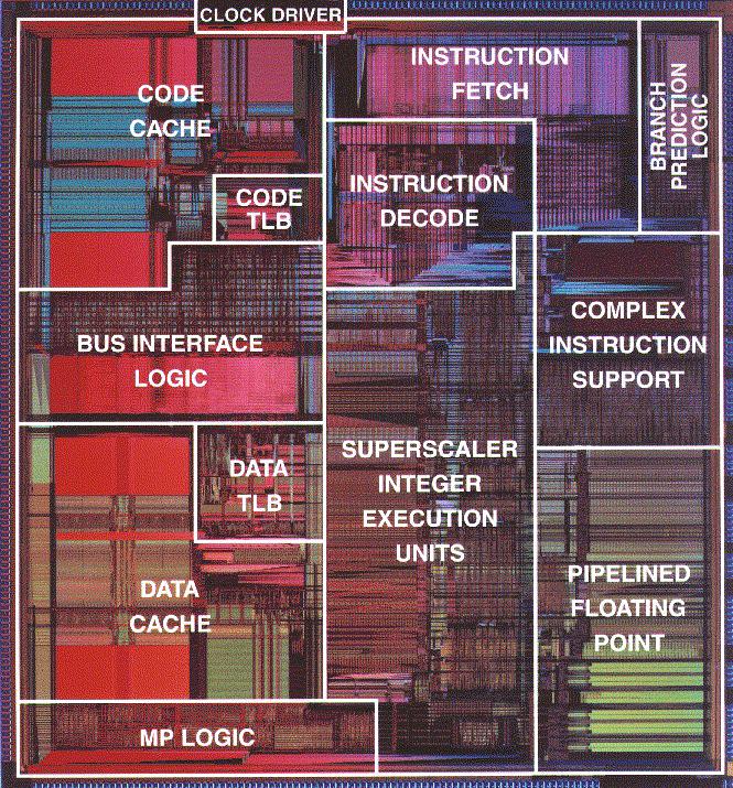
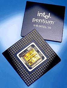
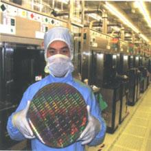
4 Integrated Circuits Information Era 4
5 5
6 Spin Coating of Photoresist 6
7 Lithography Exposure to ultraviolet light through a quartz mask. S.M. Sze, Semiconductor Devices, Wiley,
8 Semiconductor Processing UV Light Photoresist Mask (Layout) Batch Processing 8

9 Foundry Processes for Microelectromechanical Systems (MEMS) Multi-User MEMS Processes (MUMPS) Example Design Anchor hole poly2 1.5 Layers and Nominal Thickness in Microns Anchor gold 0.5 MCNC poly0 nitride oxide 1 oxide 2 nitride poly0 poly2 (a) After Poly2 Deposition (b) Released Device 9
10 Add nitride (600 nm, LPCVD (low pressure chemical vapor deposition) Silicon Substrate 100 mm, n-type, 1-2 Ohm-cm, surface doped with phosphorus 10
11 Add Poly0 (500 nm, LPCVD) Silicon Substrate 11
12 Patterning through 1st level mask (Poly0) using Photolithography Design Poly0 Patterned Photoresist Photoresist Silicon Substrate 12
13 Removal of Unwanted Poly0 using Reactive Ion Etching Design Poly0 Patterned Photoresist Silicon Substrate 13
14 1st Oxide Deposition 2 um using LPCVD Design Poly0 Silicon Substrate 14
15 Patterning through 3rd level mask (Anchor1) using Photolithography Design Anchor1 and Deep RIE Photoresist Silicon Substrate 15
16 Blanket un-doped polysilicon deposition(poly1) 2 um using LPCVD... followed by 200 nm PSG deposition and annealing at 1050 C for 1 hr Silicon Substrate 16
17 Patterning through 4th level mask (Poly1) using Photolithography... and Deep RIE Silicon Substrate PSG layer etched first to form the RIE hard mask 17
18 Release of structures using HF (46% HF, room temperature, minutes; followed by several minutes in DI water and then alcohol by at least 10 minutes in an oven at 110 C Silicon Substrate 18
19 Microelectromechanical Systems (MEMS) Multi-User MEMS Processes (MUMPS) Example Design Anchor hole poly2 1.5 Layers and Nominal Thickness in Microns Anchor gold 0.5 MCNC poly0 nitride oxide 1 oxide 2 nitride poly0 poly2 (a) After Poly2 Deposition (b) Released Device 19

20 Array of Piston Mirrors (W. D. Cowan and V. M. Bright) 20

21 MUMPs Chip 1cm 2 21
22 Electrostatic Force The energy stored at a given voltage is, U ( x, z) = 1 CV ε0ε r A = V 2 z The force between the plates in the vertical direction is, electrostatic vertical force between plates F e A F ( z) r z U ( x, z) = ε ε = = V z 2 1 z 1 2 = ε 1 0ε 2 2 r V A z 0 2 (negative z direction) 1 z z o force vs. distance is nonlinear metal dielectric air metal d The flexures can be modeled as cantilevers. For small deflections, a cantilever's restoring force is given by Hooke's law, F c = k d force vs. distance is linear where, k = flexure spring constant d = deflection distance 22
23 Restoring Force The flexure spring constant is given by, where, k = Ewt 3 L σ (1 2L 3 μ + cross-sectional spring constant E w t L σ = Young's Modulus = flexure width = flexure thickness = flexure length ) wt stress term (due to residual stress) = flexure material stress μ = flexure material Poisson's ratio The flexure spring constant is determined during device design and construction, it is not a function of voltage or deflection. The equation for k is only an approximation! For stable deflection the electrostatic force is balanced by the restorative flexure force, F = 4 e NF c where, N = number of flexures Anchor Flexure gold nitride poly0 poly2 23
24 Pull-Down Voltage assuming free space between the plates we get, AV 2 = ε0 Nkd z solving for V as a function of d gives, V = z 2 ε0 Nkd A z z ( z d ) = 0 replacing by gives, z o metal dielectric air metal d V = ( z d ) 0 2Nkd ε A 0 This equation calculates the required voltage,, to deflect the top plate of the piston actuator a distance,, from the initial plate separation, z. V d 0 24
25 Maximum Deflection Note that we are trying to balance the nonlinear electrostatic force,, with a linear force, F c. An imbalance or snap-through occurs when the rate of change in voltage vs. deflection distance is zero: dv dd d = d s = = 1 2Nk 2Nk 0 s s s 2 ε0a ε0a = ( z0 ds ) ds ds 2 2 ( z d ) d d = z0ds ds 2ds = z0ds 3ds d s = z 3 0 ds z0 where, = deflection distance from initial separation,, to snap-through. 1 2 z o metal F e dielectric air metal d deflection z z 3 Note : The rule also applies 0 to cantilevers and microbridges. 0 voltage 25
26 An Example A plate: 250 μm square An air gap: 2 μm A flexure: 40 μm x 10 μm x 0.5 μm E = 169 GPa for the flexure k = 169,000 MPa x 10 x /(4 x 40 3 ) = 0.8 μn/μm d = 1/3 x 2 μm = 0.7 μm V = (2/3 x 2μm) x SQRT [(2x1x0.8x0.7)/(8.85E-6 x )] = 1.9 V ε o = 8.85E-6 pf/μm 1 Pa = 1 Newton/m 2 = 1 N/m 2 1 MPa = 1 μn/μm 1 V = SQRT (μn x μm/pf) Anchor Flexure gold nitride poly0 poly2 k = V Ewt 3 L 4 = ( z d ) 0 σ (1 2L 3 μ + 2Nkd ε A 26 0 ) wt


27 Piston Micromirrors Evolution of a Piston Micromirror Over Four MUMPs Fabrication Runs aluminum square mirror with four flexures 60 μm wide copper hexagonal mirror 50 μm wide gold hexagonal mirror AFIT 100 μm wide gold hexagonal mirror J.H. Comtois and V.M. Bright, AFIT 27

28 Simulation of Mirror Design 28
29 Multi-User MEMS Processes (MUMPS) Example Design Mirror Accelerometer? Anchor hole poly2 1.5 Layers and Nominal Thickness in Microns Anchor gold 0.5 MCNC poly0 nitride oxide 1 oxide 2 nitride poly0 poly2 (a) After Poly2 Deposition (b) Released Device 29
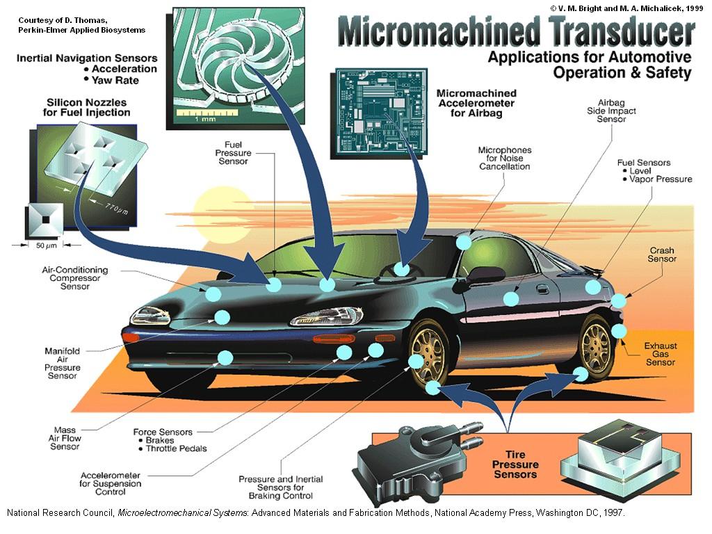
30 V. M. Bright and M. A. Michalicek, 1999 Piezoresistive Readout Sensors Static Pressure Sensor Single Axis Accelerometer Oxide Proof Mass Piezoresistor Piezoresistor Glass Support Glass Support After J. W. Gardner, Microsensors, Wiley,

31 Thermal Actuator 31

32 Thermal Actuator 32

33 Array of Thermal Actuators 33
34 Contents Microelectromechanical systems (MEMS) Surface micromachining for a mirror - electrostatic actuation - pull-down voltage - stiction - thermal actuation Bulk micromachining for a pressure sensor - processing steps -piezoresistor Applications 34


35 V. M. Bright and M. A. Michalicek, 1999 Piezoresistive Readout Sensors Static Pressure Sensor Oxide Piezoresistor Glass Support 35
36 Processing Steps for Pressure Sensor Piezoresistor Glass Support 36
37 Low Pressure Chemical Vapor Deposition (LPCVD) Gas flow of dichloro silane (DCS) and ammonia 37

38 Reactive Ion Etching Chemical and Physical Etching Si Si 3 N 4 Si 3 N 4 Piezoresistor Glass Support 38
 {111} {110} Substrate No Agitation Substrate With Agitation Substrate XeF 2, HCl, HF Si 3 N 4 {111}")
39 Etching Bulk Silicon V. M. Bright and M. A. Michalicek, 1999 Isotropic Etching Masking Material Anisotropic Etching (Two Wafer Orientations) {111} {110} Substrate No Agitation Substrate With Agitation Substrate XeF 2, HCl, HF Si 3 N 4 {111} Isotropic Si Substrate {100} Si 3 N 4 Piezoresistor Anisotropic KOH, EDP, Hydrazine After L. J. Ristic, ed., Sensor Technology and Devices, Artech House, Glass Support J. H. Comtois, Ph.D. Thesis, AFIT,
40 Piezoresistor Microcrystalline polysilicon deposited using LPCVD at ~610 C on silicon nitride. Boron-ion implantation at 30 KeV with the dose of 5X10 14 cm -2 or 5X10 14 cm -2. The doped boron was activated at 950 C for 10 min or 1050 C for 30 min. 40
 Mask Ln( N ) After S. M. Sze, Semiconductor Devices, Wiley, 1985.")
 Acceleration Tube Ion Implantation System After S. M. Sze, Semiconductor Devices, Wiley, 1985.")
41 Diffusion and Implantation of Dopants V. M. Bright and M. A. Michalicek, 1999 Dopant Gas Diffusion Dopant Profile High-Velocity Dopant Ions Implantation Dopant Profile Mask Ln( N ) Mask Ln( N ) After S. M. Sze, Semiconductor Devices, Wiley, x After S. M. Sze, Semiconductor Devices, Wiley, x Analyzer Magnet Vertical Scanner Horizontal Scanner Target Wafer Variable Slit (Beam Control) Acceleration Tube Ion Implantation System After S. M. Sze, Semiconductor Devices, Wiley, Example: Release Etch Ion Source Buried Etch Stop Region Formation of Rounded, Often Complex, Three-Dimensional Bulk Silicon Structures 41


42 Anodic Bonding Piezoresistor Glass Support Na + ions moved O molecules to form SiO2 42


43 V. M. Bright and M. A. Michalicek, 1999 Piezoresistive Readout Sensors Static Pressure Sensor Single Axis Accelerometer Oxide Proof Mass Piezoresistor Piezoresistor Glass Support Glass Support After J. W. Gardner, Microsensors, Wiley,

 X-Axis 84 db Y-Axis 81 db Z-Axis 70 db Proof Mass, Resonant Frequency X-Axis Y-Axis Z-Axis 0.")

44 V. M. Bright and K. Ishikawa, 2001 Examples of Accelerometers IMI Website; High sensitivity Large dynamic range Capacitive accelerometers M. Lemkin et al., ISSCC Digest of Technical Papers, pp , Feb Noise Floor X-Axis 110 micro-g/rt. Hz Y-Axis 160 micro-g/rt. Hz Z-Axis 990 micro-g/rt. Hz Dynamic Range (100 Hz BW) X-Axis 84 db Y-Axis 81 db Z-Axis 70 db Proof Mass, Resonant Frequency X-Axis Y-Axis Z-Axis micro-gram, 3.2kHz micro-gram, 4.2kHz micro-gram, 8.3kHz Resonant accelerometers Open view of an accelerometer assembly T. A. Roessig et al., IEEE Frequency Control Symposium, Orlando FL, May The World of Microsystems, FSRM, FSRM website;
45 45


46 Applications and Markets of MEMS in Mobile Communications Brochure of the Report from Yole Développement, Feb


47 47
48 Applications and Markets of MEMS in Mobile Communications Silicon microphone: improves the manufacturability of microphone for similar performance compared to ECM 3D accelerometers: adds functions for man machine interface and silent mode activation RF MEMS passive and active devices: provides better integration of passive devices for RF module and faster frequency agility Gyroscope for camera stabilisation and GPS: enables real digital imaging, preserves the GPS signal Microfuel cell: provides longer lifetime for the batteries Chemical and Biochip: personal weather station and health care monitor Brochure of the Report from Yole Développement, Feb
49 Silicon Microwell Polymerase Chain Reaction (PCR) 49
50 Summary Microelectromechanical systems (MEMS) Surface micromachining for a mirror - electrostatic actuation - pull-down voltage - stiction - thermal actuation Bulk micromachining for a pressure sensor - processing steps -piezoresistor Applications 50
MEMS II: January 23. Lab 1: Pop-up mirror - PolyMUMPS - Thermal actuators - Mirror CoventorWare
 MEMS II: January 23 Lab 1: Pop-up mirror - PolyMUMPS - Thermal actuators - Mirror CoventorWare Microelectromechanical Systems (MEMS) Multi-User MEMS Processes (MUMPS) Example Design Anchor hole 2.0 0.5
Lecture 10: MultiUser MEMS Process (MUMPS)
") MEMS: Fabrication Lecture 10: MultiUser MEMS Process (MUMPS) Prasanna S. Gandhi Assistant Professor, Department of Mechanical Engineering, Indian Institute of Technology, Bombay, 1 Recap Various VLSI based
MEMS: Fabrication Lecture 10: MultiUser MEMS Process (MUMPS) Prasanna S. Gandhi Assistant Professor, Department of Mechanical Engineering, Indian Institute of Technology, Bombay, 1 Recap Various VLSI based
Fabrication Technology, Part II
 EEL5225: Principles of MEMS Transducers (Fall 2003) Fabrication Technology, Part II Agenda: Process Examples TI Micromirror fabrication process SCREAM CMOS-MEMS processes Wafer Bonding LIGA Reading: Senturia,
Surface micromachining and Process flow part 1
 Surface micromachining and Process flow part 1 Identify the basic steps of a generic surface micromachining process Identify the critical requirements needed to create a MEMS using surface micromachining
EE C245 ME C218 Introduction to MEMS Design Fall 2011
 Lecture Outline EE C245 ME C218 Introduction to MEMS Design Fall 2011 Prof. Clark T.-C. Nguyen Dept. of Electrical Engineering & Computer Sciences University of California at Berkeley Berkeley, CA 94720
Dr. Lynn Fuller Webpage:
 ROCHESTER INSTITUTE OF TECHNOLOGY MICROELECTRONIC ENGINEERING Microelectromechanical Systems (MEMs) Process Integration Dr. Lynn Fuller Webpage: http://people.rit.edu/lffeee 82 Lomb Memorial Drive Rochester,
EECS130 Integrated Circuit Devices
 EECS130 Integrated Circuit Devices Professor Ali Javey 9/13/2007 Fabrication Technology Lecture 1 Silicon Device Fabrication Technology Over 10 15 transistors (or 100,000 for every person in the world)
Today s Class. Materials for MEMS
 Lecture 2: VLSI-based Fabrication for MEMS: Fundamentals Prasanna S. Gandhi Assistant Professor, Department of Mechanical Engineering, Indian Institute of Technology, Bombay, Recap: Last Class What is
4/10/2012. Introduction to Microfabrication. Fabrication
 Introduction to Microfabrication Fabrication 1 MEMS Fabrication Flow Basic Process Flow in Micromachining Nadim Maluf, An introduction to Microelectromechanical Systems Engineering 2 Thin Film Deposition
Chapter 3 Silicon Device Fabrication Technology
 Chapter 3 Silicon Device Fabrication Technology Over 10 15 transistors (or 100,000 for every person in the world) are manufactured every year. VLSI (Very Large Scale Integration) ULSI (Ultra Large Scale
Lecture 5. SOI Micromachining. SOI MUMPs. SOI Micromachining. Silicon-on-Insulator Microstructures. Agenda:
 EEL6935 Advanced MEMS (Spring 2005) Instructor: Dr. Huikai Xie SOI Micromachining Agenda: SOI Micromachining SOI MUMPs Multi-level structures Lecture 5 Silicon-on-Insulator Microstructures Single-crystal
Chapter 2 OVERVIEW OF MEMS
 6 Chapter 2 OVERVIEW OF MEMS 2.1 MEMS and Microsystems The term MEMS is an abbreviation of microelectromechanical system. MEMS contains components ofsizes in 1 micrometer to 1 millimeter. The core element
Cambridge University Press A Guide to Hands-on MEMS Design and Prototyping Joel A. Kubby Excerpt More information.
 1 Introduction 1.1 Overview of MEMS fabrication Microelectromechanical systems (MEMS) fabrication developed out of the thin-film processes first used for semiconductor fabrication. To understand the unique
EE C245 ME C218 Introduction to MEMS Design
 EE C245 ME C218 Introduction to MEMS Design Fall 2007 Prof. Clark T.-C. Nguyen Dept. of Electrical Engineering & Computer Sciences University of California at Berkeley Berkeley, CA 94720 Lecture 10: Surface
Micro-Electro-Mechanical Systems (MEMS) Fabrication. Special Process Modules for MEMS. Principle of Sensing and Actuation
 Fabrication. Special Process Modules for MEMS. Principle of Sensing and Actuation") Micro-Electro-Mechanical Systems (MEMS) Fabrication Fabrication Considerations Stress-Strain, Thin-film Stress, Stiction Special Process Modules for MEMS Bonding, Cavity Sealing, Deep RIE, Spatial forming
Micro-Electro-Mechanical Systems (MEMS) Fabrication Fabrication Considerations Stress-Strain, Thin-film Stress, Stiction Special Process Modules for MEMS Bonding, Cavity Sealing, Deep RIE, Spatial forming
Surface Micromachining
 Surface Micromachining Micro Actuators, Sensors, Systems Group University of Illinois at Urbana-Champaign Outline Definition of surface micromachining Most common surface micromachining materials - polysilicon
Welcome MNT Conference 1 Albuquerque, NM - May 2010
 Welcome MNT Conference 1 Albuquerque, NM - May 2010 Introduction to Design Outline What is MEMs Design General Considerations Application Packaging Process Flow What s available Sandia SUMMiT Overview
EE 5344 Introduction to MEMS. CHAPTER 3 Conventional Si Processing
 3. Conventional licon Processing Micromachining, Microfabrication. EE 5344 Introduction to MEMS CHAPTER 3 Conventional Processing Why silicon? Abundant, cheap, easy to process. licon planar Integrated
MEMS Fabrication. Beyond Integrated Circuits. MEMS Basic Concepts
 MEMS Fabrication Beyond Integrated Circuits MEMS Basic Concepts Uses integrated circuit fabrication techniques to make mechanical as well as electrical components on a single chip. Small size 1µm 1mm Typically
Micro-Electro-Mechanical Systems (MEMS) Fabrication. Special Process Modules for MEMS. Principle of Sensing and Actuation
 Fabrication. Special Process Modules for MEMS. Principle of Sensing and Actuation") Micro-Electro-Mechanical Systems (MEMS) Fabrication Fabrication Considerations Stress-Strain, Thin-film Stress, Stiction Special Process Modules for MEMS Bonding, Cavity Sealing, Deep RIE, Spatial forming
Micro-Electro-Mechanical Systems (MEMS) Fabrication Fabrication Considerations Stress-Strain, Thin-film Stress, Stiction Special Process Modules for MEMS Bonding, Cavity Sealing, Deep RIE, Spatial forming
Mikrosensorer. Microfabrication 1
 Mikrosensorer Microfabrication 1 Literature Introductory MEMS Fabrication and Applications Thomas M. Adams and Richard A. Layton Available as ebook on http://www.lub.lu.se/en/search/lubsearch.html This
6.777J/2.732J Design and Fabrication of Microelectromechanical Devices Spring Term Solution to Problem Set 2 (16 pts)
") 6.777J/2.732J Design and Fabrication of Microelectromechanical Devices Spring Term 2007 By Brian Taff (Adapted from work by Feras Eid) Solution to Problem Set 2 (16 pts) Issued: Lecture 4 Due: Lecture
6.777J/2.732J Design and Fabrication of Microelectromechanical Devices Spring Term 2007 By Brian Taff (Adapted from work by Feras Eid) Solution to Problem Set 2 (16 pts) Issued: Lecture 4 Due: Lecture
Review of CMOS Processing Technology
 - Scaling and Integration Moore s Law Unit processes Thin Film Deposition Etching Ion Implantation Photolithography Chemical Mechanical Polishing 1. Thin Film Deposition Layer of materials ranging from
Lecture 7 CMOS MEMS. CMOS MEMS Processes. CMOS MEMS Processes. Why CMOS-MEMS? Agenda: CMOS MEMS: Fabrication. MEMS structures can be made
 EEL6935 Advanced MEMS (Spring 2005) Instructor: Dr. Huikai Xie CMOS MEMS Agenda: Lecture 7 CMOS MEMS: Fabrication Pre-CMOS Intra-CMOS Post-CMOS Deposition Etching Why CMOS-MEMS? Smart on-chip CMOS circuitry
Czochralski Crystal Growth
 Czochralski Crystal Growth Crystal Pulling Crystal Ingots Shaping and Polishing 300 mm wafer 1 2 Advantage of larger diameter wafers Wafer area larger Chip area larger 3 4 Large-Diameter Wafer Handling
Surface Micromachining
 Surface Micromachining Outline Introduction Material often used in surface micromachining Material selection criteria in surface micromachining Case study: Fabrication of electrostatic motor Major issues
CMOS Technology. Flow varies with process types & company. Start with substrate selection. N-Well CMOS Twin-Well CMOS STI
 CMOS Technology Flow varies with process types & company N-Well CMOS Twin-Well CMOS STI Start with substrate selection Type: n or p Doping level, resistivity Orientation, 100, or 101, etc Other parameters
CS/ECE 5710/6710. N-type Transistor. N-type from the top. Diffusion Mask. Polysilicon Mask. CMOS Processing
 CS/ECE 5710/6710 CMOS Processing Addison-Wesley N-type Transistor D G +Vgs + Vds S N-type from the top i electrons - Diffusion Mask Mask for just the diffused regions Top view shows patterns that make
Proceedings Post Fabrication Processing of Foundry MEMS Structures Exhibiting Large, Out-of-Plane Deflections
 Proceedings Post Fabrication Processing of Foundry MEMS Structures Exhibiting Large, Out-of-Plane Deflections LaVern Starman 1, *, John Walton 1, Harris Hall 1 and Robert Lake 2 1 Sensors Directorate,
Solid State Sensors. Microfabrication 8/22/08 and 8/25/08
 Solid State Sensors Microfabrication 8/22/08 and 8/25/08 Purpose of This Material To introduce the student to microfabrication techniques as used to fabricate MEMS Sensors Understand concepts not specifics
MICRO-ELECTRO-MECHANICAL VARIABLE BLAZE GRATINGS
 MICRO-ELECTRO-MECHANICAL VARIABLE BLAZE GRATINGS D. M. Burns and V. M. Bright Air Force Institute of Technology Department of Electrical and Computer Engineering Wright-Patterson Air Force Base, OH 45433-7765
Process Integration. MEMS Release Techniques Sacrificial Layer Removal Substrate Undercut
 Process Integration Self-aligned Techniques LOCOS- self-aligned channel stop Self-aligned Source/Drain Lightly Doped Drain (LDD) Self-aligned silicide (SALICIDE) Self-aligned oxide gap MEMS Release Techniques
Lect. 2: Basics of Si Technology
 Unit processes Thin Film Deposition Etching Ion Implantation Photolithography Chemical Mechanical Polishing 1. Thin Film Deposition Layer of materials ranging from fractions of nanometer to several micro-meters
Doping and Oxidation
 Technische Universität Graz Institute of Solid State Physics Doping and Oxidation Franssila: Chapters 13,14, 15 Peter Hadley Technische Universität Graz Institute of Solid State Physics Doping Add donors
Lecture 3: Integrated Processes
 Lecture 3: Integrated Processes Single-Crystal Silicon Process Integration Polysilicon Micromachining Process Integrated CMOS Micromachining Process ENE 5400, Spring 2004 1 Single Crystal Silicon ENE 5400,
IC/MEMS Fabrication - Outline. Fabrication
 IC/MEMS Fabrication - Outline Fabrication overview Materials Wafer fabrication The Cycle: Deposition Lithography Etching Fabrication IC Fabrication Deposition Spin Casting PVD physical vapor deposition
Integrated Processes. Lecture Outline
 Integrated Processes Thara Srinivasan Lecture 14 Picture credit: Lemkin et al. Lecture Outline From reader Bustillo, J. et al., Surface micromachining of MEMS, pp. 1556-9. A.E. Franke et al., Polycrystalline
ME 189 Microsystems Design and Manufacture. Chapter 9. Micromanufacturing
 ME 189 Microsystems Design and Manufacture Chapter 9 Micromanufacturing This chapter will offer an overview of the application of the various fabrication techniques described in Chapter 8 in the manufacturing
Problem 1 Lab Questions ( 20 points total)
") Problem 1 Lab Questions ( 20 points total) (a) (3 points ) In our EE143 lab, we use Phosphorus for the source and drain diffusion. However, most advanced processes use Arsenic. What is the advantage of
Problem 1 Lab Questions ( 20 points total) (a) (3 points ) In our EE143 lab, we use Phosphorus for the source and drain diffusion. However, most advanced processes use Arsenic. What is the advantage of
MEMS Surface Fabrication
 ROCHESTER INSTITUTE OF TECHNOLOGY MICROELECTRONIC ENGINEERING MEMS Surface Fabrication Dr. Lynn Fuller webpage: http://people.rit.edu/lffeee Electrical and Microelectronic Engineering Rochester Institute
Preface Preface to First Edition
 Contents Foreword Preface Preface to First Edition xiii xv xix CHAPTER 1 MEMS: A Technology from Lilliput 1 The Promise of Technology 1 What Are MEMS or MST? 2 What Is Micromachining? 3 Applications and
EE C245 ME C218 Introduction to MEMS Design Fall 2007
 EE C245 ME C218 Introduction to MEMS Design Fall 2007 Prof. Clark T.-C. Nguyen Dept. of Electrical Engineering & Computer Sciences University of California at Berkeley Berkeley, CA 94720 Lecture 10: Bulk
EE 143 FINAL EXAM NAME C. Nguyen May 10, Signature:
 INSTRUCTIONS Read all of the instructions and all of the questions before beginning the exam. There are 5 problems on this Final Exam, totaling 143 points. The tentative credit for each part is given to
Mostafa Soliman, Ph.D. May 5 th 2014
 Mostafa Soliman, Ph.D. May 5 th 2014 Mostafa Soliman, Ph.D. 1 Basic MEMS Processes Front-End Processes Back-End Processes 2 Mostafa Soliman, Ph.D. Wafers Deposition Lithography Etch Chips 1- Si Substrate
Fabrication and Layout
 ECEN454 Digital Integrated Circuit Design Fabrication and Layout ECEN 454 3.1 A Glimpse at MOS Device Polysilicon Aluminum ECEN 475 4.2 1 Material Classification Insulators Glass, diamond, silicon oxide
Chapter 4 Fabrication Process of Silicon Carrier and. Gold-Gold Thermocompression Bonding
 Chapter 4 Fabrication Process of Silicon Carrier and Gold-Gold Thermocompression Bonding 4.1 Introduction As mentioned in chapter 2, the MEMs carrier is designed to integrate the micro-machined inductor
ELEC 3908, Physical Electronics, Lecture 4. Basic Integrated Circuit Processing
 ELEC 3908, Physical Electronics, Lecture 4 Basic Integrated Circuit Processing Lecture Outline Details of the physical structure of devices will be very important in developing models for electrical behavior
INTEGRATED-CIRCUIT TECHNOLOGY
 INTEGRATED-CIRCUIT TECHNOLOGY 0. Silicon crystal growth and wafer preparation 1. Processing Steps 1.1. Photolitography 1.2. Oxidation 1.3. Layer Deposition 1.4. Etching 1.5. Diffusion 1.6 Backend: assembly,
Process Flow in Cross Sections
 Process Flow in Cross Sections Process (simplified) 0. Clean wafer in nasty acids (HF, HNO 3, H 2 SO 4,...) --> wear gloves! 1. Grow 500 nm of SiO 2 (by putting the wafer in a furnace with O 2 2. Coat
Regents of the University of California 1
 Electroplating: Metal MEMS Nickel Surface-Micromachining Process Flow Photoresist Wafer Release Etchant Use electroplating to obtain metal μstructures When thick: call it LIGA Pros: fast low temp deposition,
UT Austin, ECE Department VLSI Design 2. CMOS Fabrication, Layout Rules
 2. CMOS Fabrication, Layout, Design Rules Last module: Introduction to the course How a transistor works CMOS transistors This module: CMOS Fabrication Design Rules CMOS Fabrication CMOS transistors are
EE 330 Lecture 9. IC Fabrication Technology Part 2
 EE 330 Lecture 9 IC Fabrication Technology Part 2 Quiz 8 A 2m silicon crystal is cut into wafers using a wire saw. If the wire diameter is 220um and the wafer thickness is 350um, how many wafers will this
Process Integration. NMOS Generic NMOS Process Flow. CMOS - The MOSIS Process Flow
 Process Integration Self-aligned Techniques LOCOS- self-aligned channel stop Self-aligned Source/Drain Lightly Doped Drain (LDD) Self-aligned silicide (SALICIDE) Self-aligned oxide gap MEMS Release Techniques
Surface Micromachining II
 Surface Micromachining II Dr. Thara Srinivasan Lecture 4 Picture credit: Sandia National Lab Lecture Outline Reading From reader: Bustillo, J. et al., Surface Micromachining of Microelectromechanical Systems,
Lecture #18 Fabrication OUTLINE
 Transistors on a Chip Lecture #18 Fabrication OUTLINE IC Fabrication Technology Introduction the task at hand Doping Oxidation Thin-film deposition Lithography Etch Lithography trends Plasma processing
Mechanical Engineering and Applied Mechanics University of Pennsylvania. A glimpse of MEMS. Presented to MEAM 550 (Fall 2001) students
 students") Mechanical Engineering and Applied Mechanics University of Pennsylvania A glimpse of MEMS Presented to MEAM 550 (Fall 2001) students G. K. Ananthasuresh September 17, 2001 What s in a name? Micro-Electro-Mechanical
Mechanical Engineering and Applied Mechanics University of Pennsylvania A glimpse of MEMS Presented to MEAM 550 (Fall 2001) students G. K. Ananthasuresh September 17, 2001 What s in a name? Micro-Electro-Mechanical
Microelettronica. Planar Technology for Silicon Integrated Circuits Fabrication. 26/02/2017 A. Neviani - Microelettronica
 Microelettronica Planar Technology for Silicon Integrated Circuits Fabrication 26/02/2017 A. Neviani - Microelettronica Introduction Simplified crosssection of an nmosfet and a pmosfet Simplified crosssection
Isolation Technology. Dr. Lynn Fuller
 ROCHESTER INSTITUTE OF TECHNOLOGY MICROELECTRONIC ENGINEERING Isolation Technology Dr. Lynn Fuller Motorola Professor 82 Lomb Memorial Drive Rochester, NY 14623-5604 Tel (585) 475-2035 Fax (585) 475-5041
ECE 440 Lecture 27 : Equilibrium P-N Junctions I Class Outline:
 ECE 440 Lecture 27 : Equilibrium P-N Junctions I Class Outline: Fabrication of p-n junctions Contact Potential Things you should know when you leave Key Questions What are the necessary steps to fabricate
Regents of the University of California
 Topography Issues Degradation of lithographic resolution PR step coverage, streaking Thickness differences pose problems for reduction steppers Direction of Spin PR PR PR Stringers Problematic when using
PHYS 534 (Fall 2008) Process Integration OUTLINE. Examples of PROCESS FLOW SEQUENCES. >Surface-Micromachined Beam
 Process Integration OUTLINE. Examples of PROCESS FLOW SEQUENCES. >Surface-Micromachined Beam") PHYS 534 (Fall 2008) Process Integration Srikar Vengallatore, McGill University 1 OUTLINE Examples of PROCESS FLOW SEQUENCES >Semiconductor diode >Surface-Micromachined Beam Critical Issues in Process
PHYS 534 (Fall 2008) Process Integration Srikar Vengallatore, McGill University 1 OUTLINE Examples of PROCESS FLOW SEQUENCES >Semiconductor diode >Surface-Micromachined Beam Critical Issues in Process
PROCESS FLOW AN INSIGHT INTO CMOS FABRICATION PROCESS
 Contents: VI Sem ECE 06EC63: Analog and Mixed Mode VLSI Design PROCESS FLOW AN INSIGHT INTO CMOS FABRICATION PROCESS 1. Introduction 2. CMOS Fabrication 3. Simplified View of Fabrication Process 3.1 Alternative
Microstructures using RF sputtered PSG film as a sacrificial layer in surface micromachining
 Sādhanā Vol. 34, Part 4, August 2009, pp. 557 562. Printed in India Microstructures using RF sputtered PSG film as a sacrificial layer in surface micromachining VIVEKANAND BHATT 1,, SUDHIR CHANDRA 1 and
Poly-SiGe MEMS actuators for adaptive optics
 Poly-SiGe MEMS actuators for adaptive optics Blake C.-Y. Lin a,b, Tsu-Jae King a, and Richard S. Muller a,b a Department of Electrical Engineering and Computer Sciences, b Berkeley Sensor and Actuator
HOMEWORK 4 and 5. March 15, Homework is due on Monday March 30, 2009 in Class. Answer the following questions from the Course Textbook:
 HOMEWORK 4 and 5 March 15, 2009 Homework is due on Monday March 30, 2009 in Class. Chapter 7 Answer the following questions from the Course Textbook: 7.2, 7.3, 7.4, 7.5, 7.6*, 7.7, 7.9*, 7.10*, 7.16, 7.17*,
INF5490 RF MEMS. LN02: MEMS Fabrication. Spring 2012, Oddvar Søråsen Department of Informatics, UoO
 INF5490 RF MEMS LN02: MEMS Fabrication Spring 2012, Oddvar Søråsen Department of Informatics, UoO 1 Micromachining Today s lecture Important process steps General Summary: MEMS-specific steps Examples
Regents of the University of California
 Surface-Micromachining Process Flow Photoresist Sacrificial Oxide Structural Polysilcon Deposit sacrificial PSG: Target = 2 m 1 hr. 40 min. LPCVD @450 o C Densify the PSG Anneal @950 o C for 30 min. Lithography
Chapter 2 Manufacturing Process
 Digital Integrated Circuits A Design Perspective Chapter 2 Manufacturing Process 1 CMOS Process 2 CMOS Process (n-well) Both NMOS and PMOS must be built in the same silicon material. PMOS in n-well NMOS
EE 143 MICROFABRICATION TECHNOLOGY FALL 2014 C. Nguyen PROBLEM SET #9
 Issued: Tuesday, Nov. 11, 2014 PROLEM SET #9 Due: Wednesday, Nov. 19, 2010, 8:00 a.m. in the EE 143 homework box near 140 Cory 1. The following pages comprise an actual pwell CMOS process flow with poly-to-poly
L5: Micromachining processes 1/7 01/22/02
 97.577 L5: Micromachining processes 1/7 01/22/02 5: Micromachining technology Top-down approaches to building large (relative to an atom or even a transistor) structures. 5.1 Bulk Micromachining A bulk
Lecture 8-1 MCNC/MUMPS Process
 F. G. Tseng Fall/2016, 8-1, p1 Lecture 8-1 MCNC/MUMPS Process!! MCNC/MUMPS structure Layers provided: 7.0 µm Cr/Au=0.5 poly2=1.5 ox2=0.5 poly1=2.0 ox1=2.0 Poly0=0.5 Nitride=0.5 MUMPS Cross section with
Introduction to CMOS VLSI Design. Layout, Fabrication, and Elementary Logic Design
 Introduction to CMOS VLSI Design Layout, Fabrication, and Elementary Logic Design CMOS Fabrication CMOS transistors are fabricated on silicon wafer Lithography process similar to printing press On each
Gaetano L Episcopo. Introduction to MEMS
 Gaetano L Episcopo Introduction to MEMS What are MEMS? Micro Electro Mechanichal Systems MEMS are integrated devices, or systems of devices, with microscopic parts, such as: Mechanical Parts Electrical
Lecture 1A: Manufacturing& Layout
 Introduction to CMOS VLSI Design Lecture 1A: Manufacturing& Layout David Harris Harvey Mudd College Spring 2004 Steven Levitan Fall 2008 1 The Manufacturing Process For a great tour through the IC manufacturing
Introduction to Microeletromechanical Systems (MEMS) Lecture 5 Topics. JDS Uniphase MUMPs
 Lecture 5 Topics. JDS Uniphase MUMPs") Introduction to Microeletromechanical Systems (MEMS) Lecture 5 Topics JDS Uniphase MUMPS Foundry Process and Devices Foundry Process Sequence Design Rules and Process Interactions Examples CMOS for MEMS
Introduction to Microeletromechanical Systems (MEMS) Lecture 5 Topics JDS Uniphase MUMPS Foundry Process and Devices Foundry Process Sequence Design Rules and Process Interactions Examples CMOS for MEMS
3.155J / 6.152J Micro/Nano Processing Technology TAKE-HOME QUIZ FALL TERM 2005
 3.155J / 6.152J Micro/Nano Processing Technology TAKE-HOME QUIZ FALL TERM 2005 1) This is an open book, take-home quiz. You are not to consult with other class members or anyone else. You may discuss the
SURFACE MICROMACHINING
 SURFACE MICROMACHINING Features are built up, layer by layer on the surface of a substrate. Surface micromachined devices are much smaller than bulk micromachined components. Nature of deposition process
Thomas M. Adams Richard A. Layton. Introductory MEMS. Fabrication and Applications. Springer
 Thomas M. Adams Richard A. Layton Introductory MEMS Fabrication and Applications Springer Contents Preface xiü Part I Fabrication Chapter 1: Introduction 3 1.1 What are MEMS? 3 1.2 Why MEMS? 4 1.2.1. Low
EE 330 Lecture 9. IC Fabrication Technology Part II. -Oxidation -Epitaxy -Polysilicon -Planarization -Resistance and Capacitance in Interconnects
 EE 330 Lecture 9 IC Fabrication Technology Part II -Oxidation -Epitaxy -Polysilicon -Planarization -Resistance and Capacitance in Interconnects Review from Last Time IC Fabrication Technology Crystal Preparation
Micromachining vs. Soft Fabrication
 Introduction to BioMEMS & Medical Microdevices Silicon Microfabrication Part 1 Companion lecture to the textbook: Fundamentals of BioMEMS and Medical Microdevices, by Prof., http://saliterman.umn.edu/
Chapter 4 : ULSI Process Integration (0.18 m CMOS Process)
") Chapter : ULSI Process Integration (0.8 m CMOS Process) Reference. Semiconductor Manufacturing Technology : Michael Quirk and Julian Serda (00). - (00). Semiconductor Physics and Devices- Basic Principles(/e)
Chapter : ULSI Process Integration (0.8 m CMOS Process) Reference. Semiconductor Manufacturing Technology : Michael Quirk and Julian Serda (00). - (00). Semiconductor Physics and Devices- Basic Principles(/e)
Microelectronics. Integrated circuits. Introduction to the IC technology M.Rencz 11 September, Expected decrease in line width
 Microelectronics Introduction to the IC technology M.Rencz 11 September, 2002 9/16/02 1/37 Integrated circuits Development is controlled by the roadmaps. Self-fulfilling predictions for the tendencies
5.8 Diaphragm Uniaxial Optical Accelerometer
 5.8 Diaphragm Uniaxial Optical Accelerometer Optical accelerometers are based on the BESOI (Bond and Etch back Silicon On Insulator) wafers, supplied by Shin-Etsu with (100) orientation, 4 diameter and
FABRICATION OF CMOS INTEGRATED CIRCUITS. Dr. Mohammed M. Farag
 FABRICATION OF CMOS INTEGRATED CIRCUITS Dr. Mohammed M. Farag Outline Overview of CMOS Fabrication Processes The CMOS Fabrication Process Flow Design Rules EE 432 VLSI Modeling and Design 2 CMOS Fabrication
Ajay Kumar Gautam [VLSI TECHNOLOGY] VLSI Technology for 3RD Year ECE/EEE Uttarakhand Technical University
![Ajay Kumar Gautam [VLSI TECHNOLOGY] VLSI Technology for 3RD Year ECE/EEE Uttarakhand Technical University](/thumbs/75/72824557.jpg "Ajay Kumar Gautam [VLSI TECHNOLOGY] VLSI Technology for 3RD Year ECE/EEE Uttarakhand Technical University") 2014 Ajay Kumar Gautam [VLSI TECHNOLOGY] VLSI Technology for 3RD Year ECE/EEE Uttarakhand Technical University Page1 Syllabus UNIT 1 Introduction to VLSI Technology: Classification of ICs, Scale of integration,
2014 Ajay Kumar Gautam [VLSI TECHNOLOGY] VLSI Technology for 3RD Year ECE/EEE Uttarakhand Technical University Page1 Syllabus UNIT 1 Introduction to VLSI Technology: Classification of ICs, Scale of integration,
Semiconductor Manufacturing Technology. IC Fabrication Process Overview
 Semiconductor Manufacturing Technology Michael Quirk & Julian Serda October 00 by Prentice Hall Chapter 9 IC Fabrication Process Overview /4 Objectives After studying the material in this chapter, you
Lecture 0: Introduction
 Lecture 0: Introduction Introduction Integrated circuits: many transistors on one chip. Very Large Scale Integration (VLSI): bucketloads! Complementary Metal Oxide Semiconductor Fast, cheap, low power
General Introduction to Microstructure Technology p. 1 What is Microstructure Technology? p. 1 From Microstructure Technology to Microsystems
 General Introduction to Microstructure Technology p. 1 What is Microstructure Technology? p. 1 From Microstructure Technology to Microsystems Technology p. 9 The Parallels to Microelectronics p. 15 The
A discussion of crystal growth, lithography, etching, doping, and device structures is presented in
 Chapter 5 PROCESSING OF DEVICES A discussion of crystal growth, lithography, etching, doping, and device structures is presented in the following overview gures. SEMICONDUCTOR DEVICE PROCESSING: AN OVERVIEW
CMOS Fabrication. Dr. Bassam Jamil. Adopted from slides of the textbook
 CMOS Fabrication Dr. Bassam Jamil Adopted from slides of the textbook CMOS Fabrication CMOS transistors are fabricated on silicon wafer Lithography process similar to printing press On each step, different
Microfabrication of Heterogeneous, Optimized Compliant Mechanisms SUNFEST 2001 Luo Chen Advisor: Professor G.K. Ananthasuresh
 Microfabrication of Heterogeneous, Optimized Compliant Mechanisms SUNFEST 2001 Luo Chen Advisor: Professor G.K. Ananthasuresh Fig. 1. Single-material Heatuator with selective doping on one arm (G.K. Ananthasuresh)
PHYSICAL ELECTRONICS(ECE3540) Brook Abegaz, Tennessee Technological University, Fall 2013
 Brook Abegaz, Tennessee Technological University, Fall 2013") PHYSICAL ELECTRONICS(ECE3540) Brook Abegaz, Tennessee Technological University, Fall 2013 1 Chapter 1 The Crystal Structure of Solids Physical Electronics: Includes aspects of the physics of electron movement
PHYSICAL ELECTRONICS(ECE3540) Brook Abegaz, Tennessee Technological University, Fall 2013 1 Chapter 1 The Crystal Structure of Solids Physical Electronics: Includes aspects of the physics of electron movement
EE 434 Lecture 9. IC Fabrication Technology
 EE 434 Lecture 9 IC Fabrication Technology Quiz 7 The layout of a film resistor with electrodes A and B is shown. If the sheet resistance of the film is 40 /, determine the resistance between nodes A and
Manufacturing Technologies for MEMS and SMART SENSORS
 4 Manufacturing Technologies for MEMS and SMART SENSORS Dr. H. K. Verma Distinguished Professor (EEE) Sharda University, Greater Noida (Formerly: Deputy Director and Professor of Instrumentation Indian
Applications of High-Performance MEMS Pressure Sensors Based on Dissolved Wafer Process
 Applications of High-Performance MEMS Pressure Sensors Based on Dissolved Wafer Process Srinivas Tadigadapa and Sonbol Massoud-Ansari Integrated Sensing Systems (ISSYS) Inc., 387 Airport Industrial Drive,
FABRICATION PROCESSES FOR MAGNETIC MICROACTUATORS WITH POLYSILICON FLEXURES. Jack W. Judy and Richard S. Muller
 FABRICATION PROCESSES FOR MAGNETIC MICROACTUATORS WITH POLYSILICON FLEXURES Jack W. Judy and Richard S. Muller Berkeley Sensor & Actuator Center (BSAC) Department of EECS, University of California, Berkeley,
VLSI INTRODUCTION P.VIDYA SAGAR ( ASSOCIATE PROFESSOR) Department of Electronics and Communication Engineering, VBIT
 Department of Electronics and Communication Engineering, VBIT") VLSI INTRODUCTION P.VIDYA SAGAR ( ASSOCIATE PROFESSOR) contents UNIT I INTRODUCTION: Introduction to IC Technology MOS, PMOS, NMOS, CMOS & BiCMOS technologies. BASIC ELECTRICAL PROPERTIES : Basic Electrical
VLSI INTRODUCTION P.VIDYA SAGAR ( ASSOCIATE PROFESSOR) contents UNIT I INTRODUCTION: Introduction to IC Technology MOS, PMOS, NMOS, CMOS & BiCMOS technologies. BASIC ELECTRICAL PROPERTIES : Basic Electrical
VLSI. Lecture 1. Jaeyong Chung System-on-Chips (SoC) Laboratory Incheon National University. Based on slides of David Money Harris
 Laboratory Incheon National University. Based on slides of David Money Harris") VLSI Lecture 1 Jaeyong Chung System-on-Chips (SoC) Laboratory Incheon National University Based on slides of David Money Harris Goals of This Course Learn the principles of VLSI design Learn to design
VLSI Lecture 1 Jaeyong Chung System-on-Chips (SoC) Laboratory Incheon National University Based on slides of David Money Harris Goals of This Course Learn the principles of VLSI design Learn to design