Enabling new industries with high volume manufacturing: learnings from R2R processing in wearable and flexible displays
|
|
|
- Jessie Eric Byrd
- 5 years ago
- Views:
Transcription

1 Enabling new industries with high volume manufacturing: learnings from R2R processing in wearable and flexible displays Tobias Stolley, Technologist Applied Materials WEB Coating GmbH Industiral Technologies Amsterdam, Germany 22 th June, 2016
2 Outline Short introduction to Applied Materials Corporate profile Enabling & accelerating innovation Applications & megatrends Wearable devices Key R2R processing technologies for the wearable sector R2R CVD, PVD & etch Patterning technologies R2R barrier & thin film transistor processing Barrier layers & stacks for integration in mobile & wearable displays Flexible TFT backplanes processing for active matrix microfluidic sensor arrays & low pixel density reflective displays Summary Desired areas of future collaboration 2

3 The Most Exciting Industries on Earth Applied Materials is a leading equipment supplier to the semiconductor, display, solar and related industries OUR STRENGTHS Materials engineering Customer engagement Providing differentiated device performance and yield solutions 3

4 The Global Strength of Applied Stock Ticker: Fiscal 2015 Revenue: Fiscal 2015 RD&E: AMAT 8.8 billion 1.4 billion Founded: November 10, 1967 Global Presence: Employees * : Patents: 81 locations of which 20 in EMEA ~14,600 worldwide ~2,200 in EMEA ~10,200 issued Data as of fiscal year end, October 25, 2015 *Excluding temporary and interns 4
5 Applied Material s R&D activities in EMEA Micro-nano electronics Cork, IE Micro-nano electronics Leuven, BE Display Roll to roll technologies Emerging products Alzenau, DE Fab automation software Reading, UK Display Inspection and metrology Feldkirchen, Heimstetten, DE Micro-nano electronics Grenoble, FR Solar photovoltaic Treviso, IT Inspection and metrology Rehovot, IL 9 R&D LOCATIONS ACROSS EMEA 5

6 The Roll to Roll Business Unit Based in Alzenau, Germany & focused on high rate vacuum deposition of thin films on polymeric substrates for food packaging, security & flexible electronic & display based applications 6


7 The Wearable Era Has Come! Apple Watch release changing public perception of wearable electronics Potential to be the first killer applications for flexible display Customer pull rather than technology push! Flexible display key component in most devices High end products using AMOLED frontplane Considerable market potential for EPD enabled devices Apple Watch Phosphor E-Ink Worldtime 7
 & heart rate monitoring UV dose/exposure monitoring Kind Permission: J.")
8 New Wearable Sensor Products for Healthcare Increasing number of wearable sensors on the market Shock sensors for determination of impact/blast damage Real time electrocardiograms (EEG) & heart rate monitoring UV dose/exposure monitoring Kind Permission: J. Rogers, MC10 8


9 Epidermal Electronics:- The Ultimate Form Factor Application? Epidermal electronics provide best match between exploitation of form factor and need for low cost processing Metallic strain gauge serpentine structures for EEG/ECG applications Thermal sensors for blood flow measurement based on resistors Blood oximeters based on OLED light sources & organic photodiodes Sweat analytics for body condition monitoring using microfluidics Kind Permission: J. Rogers, MC10 9

10 Roll to Roll Opportunities Form factors driving new applications: shape, size, weight, unbreakability Substrates often initially in roll form & ideal for low cost processing R2R New applications driving innovation in manufacturing and materials: Inline processing for increased productivity & reduced materials costs Compatibility with low cost imprint lithography patterning technologies Lower new invest & materials cost than S2S with photolithography (< 50% if yield assumption identical) Industry now ready to invest in new technologies for new form factor products to increase differentiation in the marketplace Critical challenges in roll-to-roll manufacturing: cost, performance, yield New platforms required to meet targets Current toolsets immature-further technology development required 10
11 11


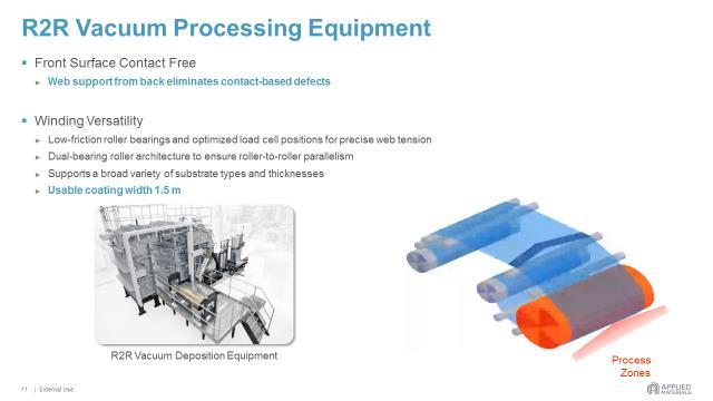
12 R2R Vacuum Processing Equipment Front Surface Contact Free Web support from back eliminates contact-based defects Winding Versatility Low-friction roller bearings and optimized load cell positions for precise web tension Dual-bearing roller architecture to ensure roller-to-roller parallelism Supports a broad variety of substrate types and thicknesses Usable coating width 1.5 m R2R Vacuum Deposition Equipment Process Zones 12

 Full web width plasma")
13 Transmission / color ratio High Density Plasma Source for PECVD Linear plasma source High-density plasma with low thermal budget High-quality film deposition Wide impedance range stability demonstrated CFD design to avoid powder buildup Laminar gas flow Uniform pressure distribution No dead or recirculation zones Plasma characteristics Plasma density > 1 x cm -3 Ion energy < 30 ev Electron temperature < 3 ev 1,4 1,2 1 0,8 0,6 0,4 0,2 0 Plasma Uniformity Web Width (mm) Full web width plasma uniformity ~± 2.5% 13


14 Rotary Cathode Technology for R2R Processing Continuous target rotation ensures clean target surface Minimized particle buildup and emission Dramatically reduced ITO & IGZO nodule density &/or target crack density Maximized process stability and target utilization (> 80 %) Reduction of heat load to substrate during deposition with rotatable Lower target surface temperature with rotatable Less risk of film overheating Higher line speed on heat sensitive, thinner gauge substrates 14


15 Roll to Roll Etch Equipment R2R dry etch tools required for selective etching of silicon based semiconductor layers & dielectrics Utilizes fluorine based chemistry Vision system required for inline microscopy & etch endpoint detection Commercial wet etchers available for source/gate/drain metal etching Requirement for selective process chemistry for etching different metals Multiple rinse step capability 200 o C Anneal Tunnel Dryer HEPA Filtered Enclosure Rated Class 100 or Better 15

16 Imprint Lithography:- Paradigm Shift in R2R Patterning Source : HP, 2009 Single mask, single imprint process with perfect source, gate & drain alignment!


17 Basic Imprint Lithography Process ~40nm lines on 50μ polyimide 1μm Multilevel structures on flex at 5m/min 20 m 4 levels in 0.5 μ step heights

18 Multilayer Barrier Stacks Low temperature inorganic layer to inhibit H 2 O and O 2 permeation Defects in each inorganic layer impact permeation Low temperature process to avoid active organic layer degradation Multilayers critical to achieve high barrier for QD and OLED devices Redundancy and increase in effective diffusion path Planarization or burying of particles, defects by organic or quasi-organic layers Ref: Flexible Flat Panel Displays, Ed. G.P. Crawford (2005). Ref:- Robert Visser MIT/Stanford Nanoforum, April

19 Multilayer Stack Barrier Performance Defect averaged barrier performance measured using Aquatran 2 permeation unit at 40 o C/100% RH conditions WVTR < 5 x 10⁻⁴ /m 2 day for full CVD 3 layer stack on PET WVTR > 10-5 /m 2 day for full CVD 3 layer stack on PEN 19


20 R2R TFT Device Performance Performance levels sufficient for sensor, EPD & electrowetting display applications High field effect mobility ~ 0.95 cm 2 /Vs for asi, ~ 10 cm 2 /Vs for IGZO High on/off current ratios ~ 10 8 for both asi and IGZO transistors Low threshold voltage ~ -2.5 V for asi & ~ 0.5 V for IGZO High threshold voltage drift stability < 0.4 V after 2000 s for asi 20
21 Summary:- R2R Processed Flexible Electronics The IoT & wearable era has arrived! Explosion in products announced on the market since 2014 Products incorporating display, communication and sense capabilities leading consumer adoption Pebble & Apple Watch paving the way for broader range of wearable fashion lead devices Display based applications show largest growth potential for vacuum processing of flexible substrates for electronics Applied s R2R tools already in high volume manufacturing for transparent materials in Touch Panel & for barrier Pilot line demonstration of R2R manufacture of complex device architectures including flexible TFT backplanes Applied Materials currently leveraging its technology portfolio & strategic partnership base to look for new high growth applications in R2R processing European research network provides new platform for open innovation in the tech sector Applied Materials using open innovation model to develop products that drive to lowest cost/m 2 manufacturing at highest performance through equipment design, scaling, metrology and yield strategies 21

22 Desired Areas of Future Collaboration Applications requiring R2R nanometer & micron level patterning for optical, decorative, electronic & automotive devices Pilot level R2R manufacturing of optical & electronic devices for wearable & IoT applications Printed & hybrid printed & vacuum processed electronics Hybrid manufacturing for IoT & medical sensors Hardcoats on roll processable substrates Inclusive optically matched hardcoats with AR functionality For further information please contact Tobias_Stolley@amat.com R2R metrology for defect detection, end point detection etc. Decorative vacuum processed &/or patterned coatings 22
23
Manipulation and control of spatial ALD layers for flexible devices. Aimcal Memphis 2016; Edward Clerkx
 Manipulation and control of spatial ALD layers for flexible devices Meyer Burger Netherlands Equipment manufacturer Functional inkjet printing Based in Eindhoven, the Netherlands Part of world-wide Meyer
Amorphous Oxide Transistor Electrokinetic Reflective Display on Flexible Glass
 Amorphous Oxide Transistor Electrokinetic Reflective Display on Flexible Glass Devin A. Mourey, Randy L. Hoffman, Sean M. Garner *, Arliena Holm, Brad Benson, Gregg Combs, James E. Abbott, Xinghua Li*,
Applied Research for Vacuum Web Coating: What is Coming Next?
 Applied Research for Vacuum Web Coating: What is Coming Next? Matthias Fahland, John Fahlteich, Steffen Günther, Manuela Junghähnel, Claus Luber, Nicolas Schiller, Cindy Steiner, Steffen Straach, Michiel
Barix Multilayers: a Water and Oxygen Barrier for Flexible Organic Electronics. Robert Jan Visser
 Barix Multilayers: a Water and Oxygen Barrier for Flexible Organic Electronics Robert Jan Visser Organic Electronics Is the Future of Electronics Organic? MIT Stanford UC Berkeley Nano Forum Vitex Systems,
Roll-to-roll Technology for Transparent High Barrier Films
 Roll-to-roll Technology for Transparent High Barrier Films Presented at the AIMCAL Fall Technical Conference, October 19-22, 2008, Myrtle Beach, SC, USA Nicolas Schiller, John Fahlteich, Matthias Fahland,
AIMCAL R2R Conference
 Contents Introduction Markets OLED Structures Technology Fabrication Process Evaluation (Microstructure & etc) Summary Introduction [Merit of Rigid OLED Display] Cheap product cost Mass production Free
Roll-to-Roll Processing Inflections for the Display & IoT Industry
 ABSTRACT Roll-to-Roll Processing Inflections for the Display & IoT Industry Neil A. Morrison, Applied Materials Web Coating GmbH, Siemensstrasse 100, 63755, Alzenau, Germany Next generation consumer electronic
The Effects of Defects on the Moisture-Barrier Performance of Clear Coatings on Polymer Substrates.
 AIMCAL, CHARLESTON, SC, 2013 The Effects of Defects on the Moisture-Barrier Performance of Clear Coatings on Polymer Substrates. The National Centre for Printed Electronics ALF part SMITH of Centre for
TFS PRODUCTION SOLUTIONS. TFS Production Solutions. For thin-film solar modules
 TFS PRODUCTION SOLUTIONS TFS Production Solutions For thin-film solar modules 2 TFS PRODUCTION SOLUTIONS MANZ AG 3 TFS PRODUCTION SOLUTIONS MANZ AG GERMAN ENGINEERING INTERNATIONALLY STAGED GLOBAL REFERENCES
Flexible functional devices at mass production level with the FLEx R2R sald platform
 Flexible functional devices at mass production level with the FLEx R2R sald platform D. Spee, W. Boonen, D. Borsa and E. Clerkx Meyer Burger (Netherlands) B.V. Meyer Burger Introduction to sald Challenges
VISION INNOVATE INSPIRE DELIVER
 INSPIRE Vision About NovaCentrix Photonic Curing INNOVATE History Applications DELIVER Our Products SimPulse Conductive Inks NanoPowders VISION NovaCentrix partners with you to take ideas from inspiration
Study on the hydrogenated ZnO-based thin film transistors
 Final Report Study on the hydrogenated ZnO-based thin film transistors To Dr. Gregg Jessen Asian Office of Aerospace Research & Development April 30th, 2011 Jae-Hyung Jang School of Information and Communications
Photovoltaics & Solar Thermals. Thin-film equipment. Customized. FHR Anlagenbau GmbH I
 Photovoltaics & Solar Thermals Thin-film equipment. Customized. FHR Anlagenbau GmbH I www.fhr.de FHR Anlagenbau GmbH is an innovative enterprise in the branch of vacuum processing and thin-film technologies.
TFS PRODUCTION SOLUTIONS. TFS Production Solutions. For thin-film solar modules
 TFS PRODUCTION SOLUTIONS TFS Production Solutions For thin-film solar modules 2 TFS PRODUCTION SOLUTIONS MANZ AG 3 TFS PRODUCTION SOLUTIONS MANZ AG GERMAN ENGINEERING INTERNATIONALLY STAGED GLOBAL REFERENCES
High Rate low pressure PECVD for barrier and optical coatings
 High Rate low pressure PECVD for barrier and optical coatings, Matthias Fahland, John Fahlteich, Björn Meyer, Steffen Straach, Nicolas Schiller Outline Introduction PECVD New developments magpecvd arcpecv
High Rate Deposition of Reactive Oxide Coatings by New Plasma Enhanced Chemical Vapor Deposition Source Technology
 General Plasma, Inc. 546 East 25th Street Tucson, Arizona 85713 tel. 520-882-5100 fax. 520-882-5165 High Rate Deposition of Reactive Oxide Coatings by New Plasma Enhanced Chemical Vapor Deposition Source
IMRE/ETPL Flagship Project
 IMRE/ETPL Flagship Project Nanoparticulate Barrier Films & Gas Permeation Measurement Techniques for Thin Film Solar & Display Application Problems Senthil Ramadas Institute of Materials Research & Engineering
Process Improvement Opportunities from New In-line Coating and Film Thickness Measurement Tools 2011 AIMCAL TECHNOLOGY OF THE YEAR
 Process Improvement Opportunities from New In-line Coating and Film Thickness Measurement Tools 2011 AIMCAL TECHNOLOGY OF THE YEAR Innovative technology enables improved coating QA The core principle behind
Progress in Roll-to-Roll Atomic Layer Deposition
 Progress in Roll-to-Roll Atomic Layer Deposition Council for Chemical Research Barrier Workshop Arlington, Virginia September 20, 2012 E. Dickey Lotus Applied Technology Outline ALD for barrier films ALD
Roll-to-roll ALD prototype for 500 mm wide webs
 Roll-to-roll ALD prototype for 500 mm wide webs Tapani Alasaarela, Mikko Söderlund, Pekka Soininen Beneq Oy, Ensimmäinen Savu, 01510 Vantaa, Finland Roll-to-roll (R2R) atomic layer deposition (ALD) technology
SINGULUS TECHNOLOGIES. SINGULUS TECHNOLOGIES AG _ Q1 Presentation
 SINGULUS TECHNOLOGIES _ Q1 Presentation May 2017 Agenda May 12, 2017-2 - 1 Overview 2 Financials 3 SINGULUS TECHNOLOGIES Segments & New Business Areas 4 SINGULUS TECHNOLOGIES Outlook SINGULUS TECHNOLOGIES
Activities in Plasma Process Technology at SENTECH Instruments GmbH, Berlin. Dr. Frank Schmidt
 Activities in Plasma Process Technology at SENTECH Instruments GmbH, Berlin Dr. Frank Schmidt The Company Company Private company, founded 1990 80 employees ISO 9001 Location Science & Technology Park,
Vacuum Deposition of High Performance Gas Barrier Materials
 Vacuum Deposition of High Performance Gas Barrier Materials H. Suttle, A. J. Topping, & H. E. Assender Department of Materials, University of Oxford, Parks Road, Oxford OX1 3PH ABSTRACT High performance
Czochralski Crystal Growth
 Czochralski Crystal Growth Crystal Pulling Crystal Ingots Shaping and Polishing 300 mm wafer 1 2 Advantage of larger diameter wafers Wafer area larger Chip area larger 3 4 Large-Diameter Wafer Handling
LOW TEMPERATURE PHOTONIC SINTERING FOR PRINTED ELECTRONICS. Dr. Saad Ahmed XENON Corporation November 19, 2015
 LOW TEMPERATURE PHOTONIC SINTERING FOR PRINTED ELECTRONICS Dr. Saad Ahmed XENON Corporation November 19, 2015 Topics Introduction to Pulsed Light Photonic sintering for Printed Electronics R&D Tools for
Bringing Permeation Barrier Technology to Application. From Ultra-High Barrier Films to Functional Films for Flexible Electronics
 Bringing Permeation Barrier Technology to Application From Ultra-High Barrier Films to Functional Films for Flexible Electronics Degradation of organic devices on plastic films Barrier layer stack 1 1
CONFERENCE EVALUATION FORM
 2015 AIMCAL Web Coating & Handling / SPE FlexPackCon CONFERENCE EVALUATION FORM To upgrade the quality of the Web Coating & Handling / FlexPackCon Conference, we would appreciate your comments. MONDAY,
EXCIMER LASER ANNEALING FOR LOW- TEMPERATURE POLYSILICON THIN FILM TRANSISTOR FABRICATION ON PLASTIC SUBSTRATES
 EXCIMER LASER ANNEALING FOR LOW- TEMPERATURE POLYSILICON THIN FILM TRANSISTOR FABRICATION ON PLASTIC SUBSTRATES G. Fortunato, A. Pecora, L. Maiolo, M. Cuscunà, D. Simeone, A. Minotti, and L. Mariucci CNR-IMM,
Roll-to-Roll Nanoimprint - 6 회 -
 Roll-to-Roll Nanoimprint - 6 회 - 목차 Click to add Title 1 Roll to Roll nanoimprint Introduction : Continuous Production System (Roll-to-Roll) Fabrication Processes Fabrication of nano roll mold 2 Case study
Chapter 3 Silicon Device Fabrication Technology
 Chapter 3 Silicon Device Fabrication Technology Over 10 15 transistors (or 100,000 for every person in the world) are manufactured every year. VLSI (Very Large Scale Integration) ULSI (Ultra Large Scale
A technology Roadmap for PV manufacturing
 A technology Roadmap for PV manufacturing Dr. Winfried Hoffmann, Applied Materials, Vice President and CTO Energy and Environmental Solutions President European Photovoltaic Industry Association (EPIA)
Cu electroplating in advanced packaging
 Cu electroplating in advanced packaging March 12 2019 Richard Hollman PhD Principal Process Engineer Internal Use Only Advancements in package technology The role of electroplating Examples: 4 challenging
Copper Interconnect Technology
 Tapan Gupta Copper Interconnect Technology i Springer Contents 1 Introduction 1 1.1 Trends and Challenges 2 1.2 Physical Limits and Search for New Materials 5 1.3 Challenges 6 1.4 Choice of Materials 7
Innovative Roll-to-Roll Equipment & Material Development Suite
 Innovative Roll-to-Roll Equipment & Material Development Suite For Next Generation Technology from Carpe Diem Technologies and the University of Massachusetts Amherst By John Berg, Dimitur Benchev, James
Inline Sputtering System for Heterojunction Cells
 GENERIS PVD Inline Sputtering System for Heterojunction Cells GENERIS PVD Inline Sputter System for ITO and Ag Deposition on Heterojunction Solar Cells Sputtering Technology at a Glance has delivered far
EE 330 Lecture 9. IC Fabrication Technology Part 2
 EE 330 Lecture 9 IC Fabrication Technology Part 2 Quiz 8 A 2m silicon crystal is cut into wafers using a wire saw. If the wire diameter is 220um and the wafer thickness is 350um, how many wafers will this
Mass Production of Clear Barriers. Requirements on Vacuum Web Coaters for Quality Assurance. Rainer Ludwig, Applied Films, Alzenau, Germany.
 Mass Production of Clear Barriers Requirements on Vacuum Web Coaters for Quality Assurance Rainer Ludwig, Applied Films, Alzenau, Germany Abstract An increasing number of packages using Transparent Barrier
Improving the Performance of Ceramic Barrier Layers used in Packaging Materials
 Improving the Performance of Ceramic Barrier Layers used in Packaging Materials Roland Trassl Senior Manager Advanced Development Applied Materials WEB Coating GmbH AIMCAL Tampa, Florida, USA 18 th October,
Metallization deposition and etching. Material mainly taken from Campbell, UCCS
 Metallization deposition and etching Material mainly taken from Campbell, UCCS Application Metallization is back-end processing Metals used are aluminum and copper Mainly involves deposition and etching,
Novel Polysulfide Substrates for Flexible Electronics. Tolis Voutsas, Ph.D. VP, Business Development Ares Materials, Inc.
 Novel Polysulfide Substrates for Flexible Electronics Tolis Voutsas, Ph.D. VP, Business Development Ares Materials, Inc. Contents 6/21/2017 2 Company overview Founded 2014, spin-out of the University of
Fully-integrated, Bezel-less Transistor Arrays Using Reversibly Foldable Interconnects and Stretchable Origami Substrates
 Electronic Supplementary Material (ESI) for Nanoscale. This journal is The Royal Society of Chemistry 2016 Fully-integrated, Bezel-less Transistor Arrays Using Reversibly Foldable Interconnects and Stretchable
AIMCAL R2R Conference
 Roll-to-Roll Integrated Deposition, Lithography, and Etching on Flexible Corning Willow Glass for Electronics Device Fabrication Robert Malay, Christian Bezama, Mark Poliks, Ming-Huang Huang, Sean Garner,
Laser Micromachining of Bulk Substrates and Thin Films Celine Bansal
 Laser Micromachining of Bulk Substrates and Thin Films Celine Bansal Oxford Lasers Ltd Moorbrook Park Didcot, Oxfordshire, OX11 7HP Tel: +44 (0) 1235 810088 www.oxfordlasers.com Outline Oxford Lasers Importance
Nanomend Acheivements
 NANOMEND METROLOGY FOR ENHANCED NANO-SCALE DETECTION, CLEANING AND REPAIR Enhanced in-line detection, cleaning and repair of nano scale defects in thin films for flexible photovoltaic and food packaging
EECS130 Integrated Circuit Devices
 EECS130 Integrated Circuit Devices Professor Ali Javey 9/13/2007 Fabrication Technology Lecture 1 Silicon Device Fabrication Technology Over 10 15 transistors (or 100,000 for every person in the world)
Transparent Ultra-Barrier Film Production and Product Integration
 Transparent Ultra-Barrier Film Production and Product Integration Mark George, Martin Rosenblum, Jason Bloking Rex Chang Vitriflex Inc., 2350 Zanker Road, Suite 20, San Jose, CA 95131 Introduction Vitriflex
Photonic Drying Pulsed Light as a low Temperature Sintering Process
 Photonic Drying Pulsed Light as a low Temperature Sintering Process Lou Panico Xenon Corporation W E S T E R N M I C H I G A N U N I V E R S I T Y PRESENTATION OVERVIEW What is Printed Electronics Materials
ITO SPUTTER COATED FILMS FOR TOUCH PANEL APPLICATIONS USING ROTARY SINTERED CERAMIC ITO TARGETS: WHAT CAN BE LEARNED FROM GLASS COATING?
 ITO SPUTTER COATED FILMS FOR TOUCH PANEL APPLICATIONS USING ROTARY SINTERED CERAMIC ITO TARGETS: WHAT CAN BE LEARNED FROM GLASS COATING? Paul Lippens AIMCAL Web coating conference 2012 Outline Introduction
Review of CMOS Processing Technology
 - Scaling and Integration Moore s Law Unit processes Thin Film Deposition Etching Ion Implantation Photolithography Chemical Mechanical Polishing 1. Thin Film Deposition Layer of materials ranging from
csi PRODUCTION SOLUTIONS csi PRODUCTION SOLUTIONS FOR CRYSTALLINE SILICON SOLAR CELLS
 csi PRODUCTION csi PRODUCTION FOR CRYSTALLINE SILICON SOLAR CELLS 3 PASSION FOR EFFICIENCY PHOTOVOLTAICS CONTENT Process machines and automation systems by Manz offer many advantages for customers in the
ENCAPSULATION OF ORGANIC LIGHT EMITTING DIODES
 ENCAPSULATION OF ORGANIC LIGHT EMITTING DIODES Bhadri Visweswaran Sigurd Wagner, James Sturm, Electrical Engineering, Princeton University, NJ Siddharth Harikrishna Mohan, Prashant Mandlik, Jeff Silvernail,
è Coating technologies and coating plant concepts for thin film liquid coating layers
 è Coating technologies and coating plant concepts for thin film liquid coating layers Andrea Glawe Technical Sales 1 Source: plastic electronics 22nd IFATCC-Congress Stresa 2010 www.coatema.de Outline
Low temperature deposition of thin passivation layers by plasma ALD
 1 Low temperature deposition of thin passivation layers by plasma ALD Bernd Gruska, SENTECH Instruments GmbH, Germany 1. SENTECH in brief 2. Low temperature deposition processes 3. SENTECH SI ALD LL System
Ultra High Barrier Coatings by PECVD
 Society of Vacuum Coaters 2014 Technical Conference Presentation Ultra High Barrier Coatings by PECVD John Madocks & Phong Ngo, General Plasma Inc., 546 E. 25 th Street, Tucson, Arizona, USA Abstract Silicon
Yung-Hui Yeh, and Bo-Cheng Kung Display Technology Center (DTC), Industrial Technology Research Institute, Hsinchu 310, Taiwan
, Industrial Technology Research Institute, Hsinchu 310, Taiwan") Amorphous In 2 O 3 -Ga 2 O 3 -ZnO Thin Film Transistors and Integrated Circuits on Flexible and Colorless Polyimide Substrates Hsing-Hung Hsieh, and Chung-Chih Wu* Graduate Institute of Electronics Engineering,
Amorphous In 2 O 3 -Ga 2 O 3 -ZnO Thin Film Transistors and Integrated Circuits on Flexible and Colorless Polyimide Substrates Hsing-Hung Hsieh, and Chung-Chih Wu* Graduate Institute of Electronics Engineering,
PEAK EFFICIENCIES WITH FALLING MANUFACTURING COSTS
 PEAK EFFICIENCIES WITH FALLING MANUFACTURING COSTS Simple and cost-effective introduction of PERC technology into the mass production of solar cells Kerstin Strauch, Florian Schwarz, Sebastian Gatz 1 Introduction
Gencoa Product Portfolio
 Gencoa offer the following range of products & process technology for the thin film industry developed over the last 20 years Planar Magnetrons Plasma Pre- Treaters Reactive Gas Controllers Gencoa Product
Semiconductor Device Fabrication
 5 May 2003 Review Homework 6 Semiconductor Device Fabrication William Shockley, 1945 The network before the internet Bell Labs established a group to develop a semiconductor replacement for the vacuum
Real-time in-process wet or dry thickness measurement of thin films and discrete layers in R2R applications
 Real-time in-process wet or dry thickness measurement of thin films and discrete layers in R2R applications Novel in-process coating thickness measurement technology Uses Ruggedized Optical Interference
Advanced Sheet-to-Sheet and Roll-to-Roll thin-film processing on ultra-thin flexible glass for flexible electronic devices
 Advanced Sheet-to-Sheet and Roll-to-Roll thin-film processing on ultra-thin flexible glass for flexible electronic devices M. Junghaehnel 1, J. Westphalen 1, F. Naumann 2, G. Lorenz 2, M. Fahland 1, S.
PATTERNING OF OXIDE THIN FILMS BY UV-LASER ABLATION
 Journal of Optoelectronics and Advanced Materials Vol. 7, No. 3, June 2005, p. 1191-1195 Invited lecture PATTERNING OF OXIDE THIN FILMS BY UV-LASER ABLATION J. Ihlemann * Laser-Laboratorium Göttingen e.v.,
Nanotechnology makes brighter LED s. Michael P.C. Watts
 Nanotechnology makes brighter LED s Michael P.C. Watts www.impattern.com Outline Why are LED s such a big deal? Brightness; lumens per watt & lumens per dollar Applications How does nanotechnology help?
Amorphous and Polycrystalline Thin-Film Transistors
 Part I Amorphous and Polycrystalline Thin-Film Transistors HYBRID AMORPHOUS AND POLYCRYSTALLINE SILICON DEVICES FOR LARGE-AREA ELECTRONICS P. Mei, J. B. Boyce, D. K. Fork, G. Anderson, J. Ho, J. Lu, Xerox
Innovative Laser Processing Technologies
 Innovative Laser Processing Technologies Reinhard Ferstl Director Sales & Marketing EMEA / Asia Corning Laser Technologies September 21, 2016 2016 Corning Incorporated Corning Market Segments and Additional
EE40 Lec 22. IC Fabrication Technology. Prof. Nathan Cheung 11/19/2009
 Suggested Reading EE40 Lec 22 IC Fabrication Technology Prof. Nathan Cheung 11/19/2009 300mm Fab Tour http://www-03.ibm.com/technology/manufacturing/technology_tour_300mm_foundry.html Overview of IC Technology
200mm Next Generation MEMS Technology update. Florent Ducrot
 200mm Next Generation MEMS Technology update Florent Ducrot The Most Exciting Industries on Earth Semiconductor Display Solar 20,000,000x reduction in COST PER TRANSISTOR in 30 years 1 20x reduction in
High Definition Selective Metallization for Printed Electronics
 High Definition Selective Metallization for Printed Electronics Wolfgang Decker VAST FILMS, Ltd. Outline Introduction of VAST FILMS What is Selective Metalization Range of Applications for Selective Metalization
_C O AT I N G M AT E R I A L S
 _COATING MATERIALS COATING MATERIALS FOR PVD THIN FILM TECHNOLOGY _GfE is a leading manufacturer of sputter targets, arc cathodes and evaporation materials used for PVD thin film technology worldwide.
EE 330 Lecture 8. IC Fabrication Technology Part II. - Oxidation - Epitaxy - Polysilicon - Interconnects
 EE 330 Lecture 8 IC Fabrication Technology Part II - Oxidation - Epitaxy - Polysilicon - Interconnects Review from Last Time MOS Transistor Bulk Source Gate Drain p-channel MOSFET Lightly-doped n-type
Advances in Intense Pulsed Light Solutions For Display Manufacturing. XENON Corporation Dr. Saad Ahmed Japan IDW 2016
 Advances in Intense Pulsed Light Solutions For Display Manufacturing XENON Corporation Dr. Saad Ahmed Japan IDW 2016 Talk Outline Introduction to Pulsed Light Applications in Display UV Curing Applications
Thin. Smooth. Diamond.
 UNCD Wafers Thin. Smooth. Diamond. UNCD Wafers - A Family of Diamond Material UNCD is Advanced Diamond Technologies (ADT) brand name for a family of thin fi lm diamond products. UNCD Aqua The Aqua series
Thin. Smooth. Diamond.
 UNCD Wafers Thin. Smooth. Diamond. UNCD Wafers - A Family of Diamond Material UNCD is Advanced Diamond Technologies (ADT) brand name for a family of thin fi lm diamond products. UNCD Aqua The Aqua series
EE 5344 Introduction to MEMS. CHAPTER 3 Conventional Si Processing
 3. Conventional licon Processing Micromachining, Microfabrication. EE 5344 Introduction to MEMS CHAPTER 3 Conventional Processing Why silicon? Abundant, cheap, easy to process. licon planar Integrated
Magnetron Sputter Cathodes planar & rotatable. Linear ion sources. Reactive gas controller & endpoint detector
 GENCOA products cover 3 sputtering related areas Magnetron Sputter Cathodes planar & rotatable Reactive gas controller & endpoint detector Linear ion sources Other activities include on-site process implementation,
Developing Enhanced Substrates for OLED SSL
 Developing Enhanced Substrates for OLED SSL DOE SSL R&D Manufacturing Workshop San Diego CA 7 May, 2014 Dr. W. Dennis Slafer MicroContinuum, Inc. 57 Smith Place Cambridge, MA 02138 www.microcontinuum.com
"ITO Film Trend for Touch Panel Applications"
 AIMCAL Web Coating Conference 2011 October 23-26 Reno, Nevada USA 1 "ITO Film Trend for Touch Panel Applications" Teijin Chemicals Ltd. Haruhiko Itoh 2 Content 1. Structure and Features of TCF 2. Touch
Low-cost, deterministic quasi-periodic photonic structures for light trapping in thin film silicon solar cells
 Low-cost, deterministic quasi-periodic photonic structures for light trapping in thin film silicon solar cells The MIT Faculty has made this article openly available. Please share how this access benefits
FABRICATION ENGINEERING MICRO- NANOSCALE ATTHE AND. Fourth Edition STEPHEN A. CAMPBELL. of Minnesota. University OXFORD UNIVERSITY PRESS
 AND FABRICATION ENGINEERING ATTHE MICRO- NANOSCALE Fourth Edition STEPHEN A. CAMPBELL University of Minnesota New York Oxford OXFORD UNIVERSITY PRESS CONTENTS Preface xiii prrt i OVERVIEW AND MATERIALS
Automation & Metrology Key technologies for high-tech production
 AUTOMATION & METROLOGY Automation & Metrology Key technologies for high-tech production 2 AUTOMATION & METROLOGY MANZ AG THE STANDARDS OF TOMORROW GROW FROM THE IDEAS AND ENTHUSIASM OF TODAY Manz AG Founded
Atomic Layer Deposition
 Atomic Layer Deposition Ville Malinen R&D Engineer Nanopinnoitteita koneenrakentajille 2010 1 Introduction 1) Overview of Beneq 2) Atomic Layer Deposition (ALD), to deposit thin films, which Are dense
Nanotechnology Principles, Applications, Careers, and Education. Copyright 2011 The Pennsylvania State University
 Nanotechnology Principles, Applications, Careers, and Education Copyright 2011 The Pennsylvania State University Outline What are the principles of nanotechnology? What are some applications? What kind
Experiences of PLD Technology for LIB Separators. PICODEON Oy. Neal White
 Experiences of PLD Technology for LIB Separators PICODEON Oy Neal White 1 Outline Introduction to Picodeon Ceramic coating rationale Separator overview Why PLD for LIB separators Current status of Picodeon
Choi, Jun-Hyuk Korea Institute of Machinery & Materials
 The 11 th US-Korea Nanosymposium Choi, Jun-Hyuk 2014. 09. 29 Korea Institute of Machinery & Materials About KIMM Nano-research Bldg Clean RM Five Research Divisions; 1. Advanced Manufacturing Sys. 2. Extreme
Flexible electronics a thin film approach. Joe Pimenoff Beneq
 Flexible electronics a thin film approach Joe Pimenoff Beneq Severe semantics Thin films are thin material layers ranging from fractions of a nanometre to several micrometres in thickness. Electronic semiconductor
IC Fabrication Technology Part III Devices in Semiconductor Processes
 EE 330 Lecture 10 IC Fabrication Technology Part III Metalization and Interconnects Parasitic Capacitances Back-end Processes Devices in Semiconductor Processes Resistors Diodes Review from Last Lecture
10. Small & Mid Cap Conference, Frankfurt, Germany ODDO SEYDLER BANK AG SINGULUS TECHNOLOGIES
 10. Small & Mid Cap Conference, Frankfurt, Germany ODDO SEYDLER BANK AG SINGULUS TECHNOLOGIES 16.02.2016 Agenda 02-2016 - 2-1 Financials 2 Overview 3 Business Overview Restructuring Concept 02-2016 - 3
Making of a Chip Illustrations
 Making of a Chip Illustrations 22nm 3D/Trigate Transistors Version April 2015 1 The illustrations on the following foils are low resolution images that visually support the explanations of the individual
Productivity versus Profitability in Vacuum Web Coating
 Productivity versus Profitability in Vacuum Web Coating Liz Josephson, Applied Films Corp. Longmont CO Dirk Hoffmann, Gerard Loebig Applied Films GmbH & Co. KG, Alzenau, Germany Market requirements Quality
AIMCAL Fall Technical Conference & 19th International Conference on Vacuum Web Coating
 AIMCAL Fall Technical Conference & 19th International Conference on Vacuum Web Coating A.G. Talma, R. Schlatmann, J.W.G. Mahy Akzo Nobel Chemicals bv, P.O. Box 9300, 6800 SB Arnhem, The Netherlands. Phone
New Dual Magnetron Plasma Source Designed For Large Area Substrate Pretreatment and Oxide Film Deposition P. Morse, R. Lovro, M. Rost, and J.
 New Dual Magnetron Plasma Source Designed For Large Area Substrate Pretreatment and Oxide Film Deposition P. Morse, R. Lovro, M. Rost, and J. German, Road Map Source Design Theory of Operation Experimental
PHS6317 NANO-ENGINEERING OF THIN FILMS
 PHS6317 NANO-ENGINEERING OF THIN FILMS Ludvik Martinu, ing., PhD Professor Chairholder: NSERC Multisectorial Industrial Research Chair in Coatings and Surface Engineering ludvik.martinu@polymtl.ca www.polymtl.ca/larfis
Graduate Student Presentations
 Graduate Student Presentations Dang, Huong Chip packaging March 27 Call, Nathan Thin film transistors/ liquid crystal displays April 4 Feldman, Ari Optical computing April 11 Guerassio, Ian Self-assembly
Lect. 2: Basics of Si Technology
 Unit processes Thin Film Deposition Etching Ion Implantation Photolithography Chemical Mechanical Polishing 1. Thin Film Deposition Layer of materials ranging from fractions of nanometer to several micro-meters
DEVELOPMENTAL BIAXIALLY-ORIENTED PEEK FILM FOR FLEXBILE ELECTRONICS
 TECHNICAL PAPER DEVELOPMENTAL BIAXIALLY-ORIENTED PEEK FILM FOR FLEXBILE ELECTRONICS HIGH TEMPERATURE CAPABILITY, FLEXIBILITY AND STRENGTH Victrex plc www.victrex.com 2 Victrex Technical Paper SHAPING FUTURE
Nanoscale Barrier Coating on BOPP Packaging Film by ALD Presented by: Dr. Johanna Lahti Senior Research Fellow Tampere University of Technology
 Nanoscale Barrier Coating on BPP Packaging Film by ALD Presented by: Dr. Johanna Lahti Senior Research Fellow Tampere University of Technology Co-authors: Kimmo Lahtinen (LUT*), Petri Johansson (TUT),
Lam Research Corporation
 Lam Research Corporation 2012 Analyst & Investor Meeting 1 Safe Harbor Statement This presentation contains certain forward looking statements, including, our ability to execute our growth strategies,
Thin Films: Sputtering Systems (Jaeger Ch 6 & Ruska Ch 7,) Can deposit any material on any substrate (in principal) Start with pumping down to high
 Can deposit any material on any substrate (in principal) Start with pumping down to high") Thin Films: Sputtering Systems (Jaeger Ch 6 & Ruska Ch 7,) Can deposit any material on any substrate (in principal) Start with pumping down to high vacuum ~10-7 torr Removes residual gases eg oxygen from
Thin Films: Sputtering Systems (Jaeger Ch 6 & Ruska Ch 7,) Can deposit any material on any substrate (in principal) Start with pumping down to high vacuum ~10-7 torr Removes residual gases eg oxygen from
Progress in Monolithic III-V/Si and towards processing III-V Devices in Silicon Manufacturing. E.A. (Gene) Fitzgerald
 Fitzgerald") Progress in Monolithic III-V/Si and towards processing III-V Devices in Silicon Manufacturing E.A. (Gene) Fitzgerald M.J. Mori, C.L.Dohrman, K. Chilukuri MIT Cambridge, MA USA Funding: MARCO IFC and Army
Progress in Monolithic III-V/Si and towards processing III-V Devices in Silicon Manufacturing E.A. (Gene) Fitzgerald M.J. Mori, C.L.Dohrman, K. Chilukuri MIT Cambridge, MA USA Funding: MARCO IFC and Army
Physical Vapor Deposition (PVD) Zheng Yang
 Zheng Yang") Physical Vapor Deposition (PVD) Zheng Yang ERF 3017, email: yangzhen@uic.edu Page 1 Major Fabrication Steps in MOS Process Flow UV light Mask oxygen Silicon dioxide photoresist exposed photoresist oxide
Physical Vapor Deposition (PVD) Zheng Yang ERF 3017, email: yangzhen@uic.edu Page 1 Major Fabrication Steps in MOS Process Flow UV light Mask oxygen Silicon dioxide photoresist exposed photoresist oxide
How to turn the promises of micro LED displays into reality?
 How to turn the promises of micro LED displays into reality? Burkhard Slischka, Co founder and CEO, ALLOS Semiconductors 14th November 2017, Huawei Optical Materials and Processing Forum 2017 Photo by