200mm Next Generation MEMS Technology update. Florent Ducrot
|
|
|
- Douglas Henry
- 6 years ago
- Views:
Transcription
1 200mm Next Generation MEMS Technology update Florent Ducrot


2 The Most Exciting Industries on Earth Semiconductor Display Solar 20,000,000x reduction in COST PER TRANSISTOR in 30 years 1 20x reduction in COST PER AREA in 15 years 2 3x reduction in COST PER WATT in 4 years At 1976 transistor prices, an ipod would have cost $3.2B 1 Source: SIA, IC Knowledge LLC 2 Source: Display Search, Nikkei BP, Applied Materials


3 Continued Technology Development 200mm market growth driven by consumer electronics, automotive, industrial and medical applications LED TFB & Others Discrete Power MEMS Analog APPLIED MATERIALS Over 40 years of technology development to enable life-changing innovations * All images used with owners permission


 RF")


4 Expansion of MEMS Capabilities Applied Materials Supports MEMS Production and R&D DEVELOPING NEW EQUIPMENT, MATERIALS AND PROCESSES FOR MEMS Aluminum Nitride (AlN) Thick Aluminum (Al) RF and Mechanical Applications High Power Devices Sub-Micron MEMS Working within the Global MEMS Community


5 200mm MEMS Equipment Portfolio Applied Materials is growing its 200mm MEMS portfolio

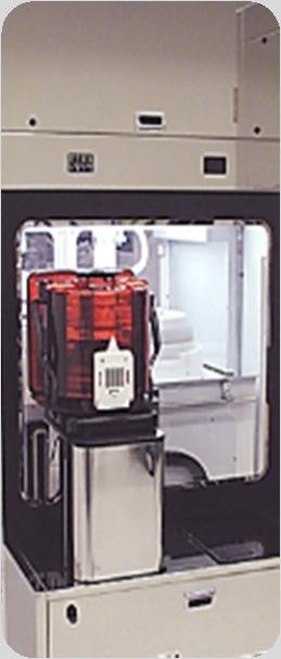
6 Latest DRIE Technologies NEW DPS DTM DRIE Chamber for MEMS, Power Devices and TSV No In-Situ Chamber Clean allows best in class wafer throughput and extends Mean Time Between Cleans far beyond 500 RF Hrs! Tunable Source Coil Technology enables WIW etch depth and sidewall profile nu. < 2 % Hard Mask-Open Capability with dielectric etch rates approaching 750nm/min! High Speed Gas Switching enabling Bosch process with << 1sec etch and deposition times Low Temperature (-20 C) Capability for increased selectivity and sidewall profile control Demo Ready Pulsed High Power Low Frequency Generator eliminating undercut on SOI wafers Parameter Ramping with enhanced recipe control New DPS DTM Chamber (Actual Photo Shown)


 and")
7 Next Generation DRIE Capability Demo Ready High Etch Rates ( 22µm/min) and Fine Profile Control for TSV Ultra-High Aspect Ratio Sub-Micron MEMS Applications 400 nm Excellent End Point and Notch Control in SOI Applications! Low Mask Undercut (17nm) and Ultra-Small Sidewall Scallops (13nm) 7


 Thick ( 40µm) CVD SiO 2")
8 Advanced Deposition Processes Adding new film processes in support of MEMS Demo Ready ECD Metal (>100µm) Single Step ( 10µm) Low Temp SiGe Epi-Silicon ( 50µm) SiO 2 Layer Ge Layer Al Layer Silicon Si Layer PVD AlN ( 2.5µm) (nu. << 0.5%) Thick ( 40µm) CVD SiO 2 High Dep Rate PVD Ge
9 Conclusion Applied Materials currently offers DRIE, CVD, PVD, CMP and Metrology Tools for MEMS. Applied Materials is continuing to expand its MEMS product portfolio with the aim of providing a complete MEMS solution in support of all process technologies that are critical to MEMS development. For More information about Applied Materials MEMS product portfolio please contact Applied Materials Sales. Applied Materials Confidential 9

10

11 MEMS CVD SiGe Demo Ready Offering Low Temp, High Dep Rate Films for CMOS Compatible MEMS Parameters Target Requirement Actual Wafer to wafer uniformity +/- 5% <3% Within wafer uniformity +/-3% <2% 1 sigma Ge content 60 65% 60% Thickness 5 10um 10µm Conformality Fill 2:1 aspect ratio TBD SiGe Layer on SiH 4 USG Maximum temperature 425C 420C Deposition rate >100nm/min 236nm/min Resistivity < 5mΩ-cm < 4 mω-cm Residual stress MPa comp 130MPa comp Strain gradient < 5x10⁻⁵ µm -1 TBD Currently the only Single Step/Pass Process For Low Temp, Thick SiGe Films! SiGe Layer on Thermal SiGe Seed 11
12 MEMS CVD Thick Oxide Demo Ready PECVD TEOS Or SiH 4 based Low Temperature, Thick Oxide ( 22µm) Parameters TEOS SiH 4 Within wafer uniformity 1.18 % 0.98 % Thickness per Pass >5 um >5 um Maximum temperature 350 C 350 C Deposition rate >1300 nm/min >2300 nm/min Residual stress -43 MPa -48 MPa Refractive Index Defects 138 (> 0.2um) 20 (> 0.2um) 20µm Thick PECVD TEOS Single pass 5µm deposition, no clean required Target Applications Include: MEMS Photonics 12
13 Aluminum Nitride (AlN) Demo Ready Oct 12 AlN for Production at Both 6 and 8 Wafer Sizes Parameters Target Requirement WIW Uniformity (6 / 8 ) < 0.5% / <1.0 % Actual < 0.5 % (6 ) << 1% (8 ) Thickness 800nm 2.5µm Tunable Deposition rate >80 nm/min > 85nm/min FWHM Rocking Curve Maximum temperature 450 C 400 C Stress -100MPa to 400MPa Tunable Refractive Index 2.08 ± Surface Roughness < 2.5nm 1.5nm AlN Layer on Mo (Deposited on 8 Wafer) Applications in RF Devices and MEMS Actuator Devices 13

 ~ 48 Si Layer Surface Roughness ~3.")
14 PVD Ge Films High Deposition Rate Ge Process For Thick Ge Films Demo Ready Parameters Actual WIW Uniformity < 2.6 % Ge Layer Thickness Deposition rate 540nm > 260 nm/min Al Layer Maximum temperature < 400 C Stress 221 MPa Bulk Resistivity (Ohm.cm) ~ 48 Si Layer Surface Roughness ~3.78 nm Often used as a Bonding Layer and Electrical Interconnect Tilted View of Top Surface Roughness ~ 3.78nm 14
Extending Etch and Deposition Capabilities for Implementation of 3D Packaging of MEMS in Volume Production
 Extending Etch and Deposition Capabilities for Implementation of 3D Packaging of MEMS in Volume Production David Butler, VP Product Management & Marketing SPTS Technologies Contents Industry Trends TSV
CMOS Technology. Flow varies with process types & company. Start with substrate selection. N-Well CMOS Twin-Well CMOS STI
 CMOS Technology Flow varies with process types & company N-Well CMOS Twin-Well CMOS STI Start with substrate selection Type: n or p Doping level, resistivity Orientation, 100, or 101, etc Other parameters
Chapter 3 Silicon Device Fabrication Technology
 Chapter 3 Silicon Device Fabrication Technology Over 10 15 transistors (or 100,000 for every person in the world) are manufactured every year. VLSI (Very Large Scale Integration) ULSI (Ultra Large Scale
Activities in Plasma Process Technology at SENTECH Instruments GmbH, Berlin. Dr. Frank Schmidt
 Activities in Plasma Process Technology at SENTECH Instruments GmbH, Berlin Dr. Frank Schmidt The Company Company Private company, founded 1990 80 employees ISO 9001 Location Science & Technology Park,
3D technologies for integration of MEMS
 3D technologies for integration of MEMS, Fraunhofer Institute for Electronic Nano Systems Folie 1 Outlook Introduction 3D Processes Process integration Characterization Sample Applications Conclusion Folie
SKW Wafer Product List
 SKW Wafer Product List Regularly updated (2.13.2018) SKW Associates, INC. 2920 Scott Blvd, Santa Clara, CA 95054 Tel: 408-919-0094, Fax: 408-919-0097 I. Available Wafers in 200mm and 300mm - Please refer
HOMEWORK 4 and 5. March 15, Homework is due on Monday March 30, 2009 in Class. Answer the following questions from the Course Textbook:
 HOMEWORK 4 and 5 March 15, 2009 Homework is due on Monday March 30, 2009 in Class. Chapter 7 Answer the following questions from the Course Textbook: 7.2, 7.3, 7.4, 7.5, 7.6*, 7.7, 7.9*, 7.10*, 7.16, 7.17*,
Czochralski Crystal Growth
 Czochralski Crystal Growth Crystal Pulling Crystal Ingots Shaping and Polishing 300 mm wafer 1 2 Advantage of larger diameter wafers Wafer area larger Chip area larger 3 4 Large-Diameter Wafer Handling
Chapter 5 Thermal Processes
 Chapter 5 Thermal Processes 1 Topics Introduction Hardware Oxidation Diffusion Annealing Post-Implantation Alloying Reflow High Temp CVD Epi Poly Silicon Nitride RTP RTA RTP Future Trends 2 Definition
New Materials as an enabler for Advanced Chip Manufacturing
 New Materials as an enabler for Advanced Chip Manufacturing Drive Innovation, Deliver Excellence ASM International Analyst and Investor Technology Seminar Semicon West July 10 2013 Outline New Materials:
Metallizing High Aspect Ratio TSVs For MEMS Challenges and Capabilities. Vincent Mevellec, PhD
 Metallizing High Aspect Ratio TSVs For MEMS Challenges and Capabilities Vincent Mevellec, PhD Agenda Introduction MEMS and sensors market TSV integration schemes Process flows for TSV Metallization aveni
Examples of dry etching and plasma deposition at Glasgow University
 Examples of dry etching and plasma deposition at Glasgow University Glasgow has pioneered and established many novel research activities involving the development of new dry etch processes and dry etch
CMP for Thru-Silicon Vias TSV Overview & Examples March 2009
 CMP for Thru-Silicon Vias TSV Overview & Examples March 2009 Packaging Evolution Source: Yole Dev 2007 2 3D Integration Source: Yole Dev 2007 Growth rates for 3D integration Flash continues to drive the
A Deep Silicon RIE Primer Bosch Etching of Deep Structures in Silicon
 A Deep Silicon RIE Primer Bosch Etching of Deep Structures in Silicon April 2009 A Deep Silicon RIE Primer 1.0) Etching: Silicon does not naturally etch anisotropically in fluorine based chemistries. Si
ADVANCES IN ETCH AND DEPOSITION TECHNOLOGIES FOR 2.5 AND 3D BEOL PROCESSING
 ADVANCES IN ETCH AND DEPOSITION TECHNOLOGIES FOR 2.5 AND 3D BEOL PROCESSING Keith Buchanan, Dave Thomas, Hefin Griffiths, Kathrine Crook, Daniel Archard, Mark Carruthers, Steve Burgess, Stephen Vargo SPTS
Today s Class. Materials for MEMS
 Lecture 2: VLSI-based Fabrication for MEMS: Fundamentals Prasanna S. Gandhi Assistant Professor, Department of Mechanical Engineering, Indian Institute of Technology, Bombay, Recap: Last Class What is
Progress in Monolithic III-V/Si and towards processing III-V Devices in Silicon Manufacturing. E.A. (Gene) Fitzgerald
 Fitzgerald") Progress in Monolithic III-V/Si and towards processing III-V Devices in Silicon Manufacturing E.A. (Gene) Fitzgerald M.J. Mori, C.L.Dohrman, K. Chilukuri MIT Cambridge, MA USA Funding: MARCO IFC and Army
Progress in Monolithic III-V/Si and towards processing III-V Devices in Silicon Manufacturing E.A. (Gene) Fitzgerald M.J. Mori, C.L.Dohrman, K. Chilukuri MIT Cambridge, MA USA Funding: MARCO IFC and Army
TSV Formation: Drilling and Filling
 3D Architectures for Semiconductor Integration and Packaging (3D ASIP), Burlingame, CA, Dec. 10-12, 2014 Preconference symposium- 3D Integration: 3D Process Technology TSV Formation: Drilling and Filling
Surface Micromachining
 Surface Micromachining Micro Actuators, Sensors, Systems Group University of Illinois at Urbana-Champaign Outline Definition of surface micromachining Most common surface micromachining materials - polysilicon
Chapter 4 Fabrication Process of Silicon Carrier and. Gold-Gold Thermocompression Bonding
 Chapter 4 Fabrication Process of Silicon Carrier and Gold-Gold Thermocompression Bonding 4.1 Introduction As mentioned in chapter 2, the MEMs carrier is designed to integrate the micro-machined inductor
INTEGRATED-CIRCUIT TECHNOLOGY
 INTEGRATED-CIRCUIT TECHNOLOGY 0. Silicon crystal growth and wafer preparation 1. Processing Steps 1.1. Photolitography 1.2. Oxidation 1.3. Layer Deposition 1.4. Etching 1.5. Diffusion 1.6 Backend: assembly,
Thin. Smooth. Diamond.
 UNCD Wafers Thin. Smooth. Diamond. UNCD Wafers - A Family of Diamond Material UNCD is Advanced Diamond Technologies (ADT) brand name for a family of thin fi lm diamond products. UNCD Aqua The Aqua series
Thin. Smooth. Diamond.
 UNCD Wafers Thin. Smooth. Diamond. UNCD Wafers - A Family of Diamond Material UNCD is Advanced Diamond Technologies (ADT) brand name for a family of thin fi lm diamond products. UNCD Aqua The Aqua series
Procese de depunere in sistemul Plasma Enhanced Chemical Vapor Deposition (PECVD)
") Procese de depunere in sistemul Plasma Enhanced Chemical Vapor Deposition (PECVD) Ciprian Iliescu Conţinutul acestui material nu reprezintă in mod obligatoriu poziţia oficială a Uniunii Europene sau a
Procese de depunere in sistemul Plasma Enhanced Chemical Vapor Deposition (PECVD) Ciprian Iliescu Conţinutul acestui material nu reprezintă in mod obligatoriu poziţia oficială a Uniunii Europene sau a
New Applications of CMP for Non-Traditional Semiconductor Manufacturing. Robert L. Rhoades, Ph.D. Entrepix, Inc.
 New Applications of CMP for Non-Traditional Semiconductor Manufacturing Robert L. Rhoades, Ph.D. Entrepix, Inc. Outline Introduction New Applications of CMP MEMS Non-CMOS Devices New Materials Epitaxial
Lect. 2: Basics of Si Technology
 Unit processes Thin Film Deposition Etching Ion Implantation Photolithography Chemical Mechanical Polishing 1. Thin Film Deposition Layer of materials ranging from fractions of nanometer to several micro-meters
Lecture 030 Integrated Circuit Technology - I (5/8/03) Page 030-1
 Page 030-1") Lecture 030 Integrated Circuit Technology - I (5/8/03) Page 030-1 LECTURE 030 INTEGRATED CIRCUIT TECHNOLOGY - I (References [7,8]) Objective The objective of this presentation is: 1.) Illustrate integrated
Lecture 030 Integrated Circuit Technology - I (5/8/03) Page 030-1 LECTURE 030 INTEGRATED CIRCUIT TECHNOLOGY - I (References [7,8]) Objective The objective of this presentation is: 1.) Illustrate integrated
Low Temperature Dielectric Deposition for Via-Reveal Passivation.
 EMPC 2013, September 9-12, Grenoble; France Low Temperature Dielectric Deposition for Via-Reveal Passivation. Kath Crook, Mark Carruthers, Daniel Archard, Steve Burgess, Keith Buchanan SPTS Technologies,
TSV Interposer Process Flow with IME 300mm Facilities
 TSV Interposer Process Flow with IME 300mm Facilities Property of Institute of Microelectronics (IME)-Singapore August 17, 2012 Outline 1. TSV interposer (TSI) cross sectional schematic TSI with BEOL,
EE C245 ME C218 Introduction to MEMS Design Fall 2011
 Lecture Outline EE C245 ME C218 Introduction to MEMS Design Fall 2011 Prof. Clark T.-C. Nguyen Dept. of Electrical Engineering & Computer Sciences University of California at Berkeley Berkeley, CA 94720
Si DRIE APPLICATION In Corial 210IL
 Si DRIE APPLICATION In Corial 210IL CORIAL 210IL ICP-RIE equipment for deep Si etching applications Enlarged functionality with capability to deep etch silicon, silicon carbide, glass, sapphire, and quartz
ME 141B: The MEMS Class Introduction to MEMS and MEMS Design. Sumita Pennathur UCSB
 ME 141B: The MEMS Class Introduction to MEMS and MEMS Design Sumita Pennathur UCSB Outline today Introduction to thin films Oxidation Deal-grove model CVD Epitaxy Electrodeposition 10/6/10 2/45 Creating
Microstructure of Electronic Materials. Amorphous materials. Single-Crystal Material. Professor N Cheung, U.C. Berkeley
 Microstructure of Electronic Materials Amorphous materials Single-Crystal Material 1 The Si Atom The Si Crystal diamond structure High-performance semiconductor devices require defect-free crystals 2 Crystallographic
New CMP Applications And Opportunities for Improvement. Robert L. Rhoades, Ph.D. Presentation for Levitronix Conference May 2011
 New CMP Applications And Opportunities for Improvement Robert L. Rhoades, Ph.D. Presentation for Levitronix Conference May 2011 Outline Background TSV s Diamond CMP Opportunities for Improvement Summary
MEMS Devices. Fraunhofer Institute for Silicon Technology ISIT. Itzehoe, Germa. any
 Examples of CMP Processess for the Manufacturing of MEMS Devices Gerfried Zwicke er Fraunhofer Institute for Silicon Technology ISIT Itzehoe, Germa any gerfried.zwicker@isit.fraunhofer.de Contents MEMS
New approaches to classical Silicon Solar Cells
 New approaches to classical Silicon Solar Cells The SSTEP Project Solar-grade Silicon by Transfer and EPitaxy G.Amato - INRIM, Torino G. Borionetti- MEMC, Novara Contents 1. What s the porous Si? 2. Epitaxy
EE 143 CMOS Process Flow
 EE 143 CMOS rocess Flow CT 84 D D G Sub G Sub S S G D S G D S + + + + - MOS Substrate Well - MOS Substrate EE 143 CMOS rocess Flow CT 85 hotoresist Si 3 4 SiO 2 Substrate selection: moderately high resistivity,
Tapered Walls Via Holes Manufactured Using DRIE Variable Isotropy Process
 Tapered Walls Via Holes Manufactured Using DRIE Variable Isotropy Process D. VASILACHE, S. RONCHIN, S. COLPO, B. MARGESIN, F. GIACOMOZZI, S. GENNARO FBK-irst, via Sommarive 18-38123 Trento, Italy; Tel.:
Silicon Epitaxial CVD Want to create very sharp PN boundary grow one type layer on other in single crystal form High dopant layers on low dopant
 Silicon Epitaxial CVD Want to create very sharp PN boundary grow one type layer on other in single crystal form High dopant layers on low dopant substrate Creates latch up protection for CMOS Buried Epi
IC/MEMS Fabrication - Outline. Fabrication
 IC/MEMS Fabrication - Outline Fabrication overview Materials Wafer fabrication The Cycle: Deposition Lithography Etching Fabrication IC Fabrication Deposition Spin Casting PVD physical vapor deposition
EECS130 Integrated Circuit Devices
 EECS130 Integrated Circuit Devices Professor Ali Javey 9/13/2007 Fabrication Technology Lecture 1 Silicon Device Fabrication Technology Over 10 15 transistors (or 100,000 for every person in the world)
Microstructures using RF sputtered PSG film as a sacrificial layer in surface micromachining
 Sādhanā Vol. 34, Part 4, August 2009, pp. 557 562. Printed in India Microstructures using RF sputtered PSG film as a sacrificial layer in surface micromachining VIVEKANAND BHATT 1,, SUDHIR CHANDRA 1 and
Silicon Epitaxial CVD Want to create very sharp PN boundary grow one type layer on other in single crystal form High dopant layers on low dopant
 Silicon Epitaxial CVD Want to create very sharp PN boundary grow one type layer on other in single crystal form High dopant layers on low dopant substrate Creates latch up protection for CMOS Buried Epi
TSV Processing and Wafer Stacking. Kathy Cook and Maggie Zoberbier, 3D Business Development
 TSV Processing and Wafer Stacking Kathy Cook and Maggie Zoberbier, 3D Business Development Outline Why 3D Integration? TSV Process Variations Lithography Process Results Stacking Technology Wafer Bonding
Micro-Electro-Mechanical Systems (MEMS) Fabrication. Special Process Modules for MEMS. Principle of Sensing and Actuation
 Fabrication. Special Process Modules for MEMS. Principle of Sensing and Actuation") Micro-Electro-Mechanical Systems (MEMS) Fabrication Fabrication Considerations Stress-Strain, Thin-film Stress, Stiction Special Process Modules for MEMS Bonding, Cavity Sealing, Deep RIE, Spatial forming
Micro-Electro-Mechanical Systems (MEMS) Fabrication Fabrication Considerations Stress-Strain, Thin-film Stress, Stiction Special Process Modules for MEMS Bonding, Cavity Sealing, Deep RIE, Spatial forming
EE40 Lec 22. IC Fabrication Technology. Prof. Nathan Cheung 11/19/2009
 Suggested Reading EE40 Lec 22 IC Fabrication Technology Prof. Nathan Cheung 11/19/2009 300mm Fab Tour http://www-03.ibm.com/technology/manufacturing/technology_tour_300mm_foundry.html Overview of IC Technology
Poly-SiGe MEMS actuators for adaptive optics
 Poly-SiGe MEMS actuators for adaptive optics Blake C.-Y. Lin a,b, Tsu-Jae King a, and Richard S. Muller a,b a Department of Electrical Engineering and Computer Sciences, b Berkeley Sensor and Actuator
EE 330 Lecture 9. IC Fabrication Technology Part II. -Oxidation -Epitaxy -Polysilicon -Planarization -Resistance and Capacitance in Interconnects
 EE 330 Lecture 9 IC Fabrication Technology Part II -Oxidation -Epitaxy -Polysilicon -Planarization -Resistance and Capacitance in Interconnects Review from Last Time Etching Dry etch (anisotropic) SiO
Complementary Metal Oxide Semiconductor (CMOS)
") Technische Universität Graz Institute of Solid State Physics Complementary Metal Oxide Semiconductor (CMOS) Franssila: Chapters 26,28 Technische Universität Graz Institute of Solid State Physics Complementary
Technische Universität Graz Institute of Solid State Physics Complementary Metal Oxide Semiconductor (CMOS) Franssila: Chapters 26,28 Technische Universität Graz Institute of Solid State Physics Complementary
Atomic Layer Deposition(ALD)
") Atomic Layer Deposition(ALD) AlO x for diffusion barriers OLED displays http://en.wikipedia.org/wiki/atomic_layer_deposition#/media/file:ald_schematics.jpg Lam s market-leading ALTUS systems combine CVD
Atomic Layer Deposition(ALD) AlO x for diffusion barriers OLED displays http://en.wikipedia.org/wiki/atomic_layer_deposition#/media/file:ald_schematics.jpg Lam s market-leading ALTUS systems combine CVD
National Nano Fabrication Centre (NNFC)
") National Nano Fabrication Centre (NNFC) Tool and Process Capabilities 1. Lithography 1.1 Direct Laser Writer/Lithography 1.1.1 Preferred Design file format: GDS2 or CIF 1.1.2 Please note that coloured
National Nano Fabrication Centre (NNFC) Tool and Process Capabilities 1. Lithography 1.1 Direct Laser Writer/Lithography 1.1.1 Preferred Design file format: GDS2 or CIF 1.1.2 Please note that coloured
Semiconductor Manufacturing Technology. IC Fabrication Process Overview
 Semiconductor Manufacturing Technology Michael Quirk & Julian Serda October 00 by Prentice Hall Chapter 9 IC Fabrication Process Overview /4 Objectives After studying the material in this chapter, you
Corial PS200 4-sided multi-module platform
 Corial PS200 4-sided multi-module platform Single wafer platform equipped with 200 mm modules Integration of ICP-CVD or PECVD process chambers Fully automated platform with cassette-to-cassette handler
EE 330 Lecture 8. IC Fabrication Technology Part II. - Oxidation - Epitaxy - Polysilicon - Interconnects
 EE 330 Lecture 8 IC Fabrication Technology Part II - Oxidation - Epitaxy - Polysilicon - Interconnects Review from Last Time MOS Transistor Bulk Source Gate Drain p-channel MOSFET Lightly-doped n-type
Deposition Technologies for >500GB/in 2 and HAMR Write Heads PMR
 Deposition Technologies for >500GB/in 2 and HAMR Write Heads PMR Outline Background New technologies for PMR pole deposition Optical films for HAMR write heads Summary 2 Background Technology Roadmap 2009
VLSI Technology. By: Ajay Kumar Gautam
 By: Ajay Kumar Gautam Introduction to VLSI Technology, Crystal Growth, Oxidation, Epitaxial Process, Diffusion Process, Ion Implantation, Lithography, Etching, Metallization, VLSI Process Integration,
Surface micromachining and Process flow part 1
 Surface micromachining and Process flow part 1 Identify the basic steps of a generic surface micromachining process Identify the critical requirements needed to create a MEMS using surface micromachining
Improving AlN & ScAlN Thin Film Technology for Next Generation PiezoMEMS SEMICON Taiwan MEMS FORUM
 Improving AlN & ScAlN Thin Film Technology for Next Generation PiezoMEMS SEMICON Taiwan 2016 - MEMS FORUM Nick Knight PVD Product Manager, SPTS Technologies SPTS Technologies A leading manufacturer of
Drytech Quad Etch Recipes Dr. Lynn Fuller Mike Aquilino Microelectronic Engineering
 ROCHESTER INSTITUTE OF TECHNOLOGY MICROELECTRONIC ENGINEERING Drytech Quad Etch Recipes Dr. Lynn Fuller Mike Aquilino 82 Lomb Memorial Drive Rochester, NY 14623-5604 Tel (585) 475-2035 Fax (585) 475-5041
Fabrication Technology, Part II
 EEL5225: Principles of MEMS Transducers (Fall 2003) Fabrication Technology, Part II Agenda: Process Examples TI Micromirror fabrication process SCREAM CMOS-MEMS processes Wafer Bonding LIGA Reading: Senturia,
Overview of CMP for TSV Applications. Robert L. Rhoades, Ph.D. Presentation for AVS Joint Meeting June 2013 San Jose, CA
 Overview of CMP for TSV Applications Robert L. Rhoades, Ph.D. Presentation for AVS Joint Meeting June 2013 San Jose, CA Outline TSV s and the Role of CMP TSV Pattern and Fill TSV Reveal (non-selective)
Fabrication of Nanoscale Silicon Membranes on SOI Wafers Using Photolithography and Selective Etching Techniques:
 Fabrication of Nanoscale Silicon Membranes on SOI Wafers Using Photolithography and Selective Etching Techniques: Participant Names: Moriah Faint, Marcos Rodriguez Mentor: Frank Tsang Date: 1 Introduction
CMP Process Development for the Via- Middle 3D TSV Applications at 28nm Technology Node
 CMP Process Development for the Via- Middle 3D TSV Applications at 28nm Technology Node UMC/ ATD_AM / CMP Department T. C. Tsai, W. C. Tsao, Welch Lin, C. L. Hsu, C. L. Lin, C. M. Hsu, J. F. Lin, C. C.
The Berkeley Marvell NanoLab
 The History The Berkeley Marvell NanoLab The Culture The Present The BNLA The Capabilities The End MEMS Industry Group M2M 20May2014 Bill Flounders, Ph.D. NanoLabExecutive Director The History The Berkeley
Design Handbook. amems Process Technology. A RSC MEMS Technology. Rockwell Scientific Company, LLC. Revision 1.0
 Design Handbook amems Process Technology A RSC MEMS Technology Rockwell Scientific Company, LLC Revision 1.0 Copyright 2005 Rockwell Scientific Company, LLC. All rights reserved. Pyrex and Vycor are trademarks
Welcome MNT Conference 1 Albuquerque, NM - May 2010
 Welcome MNT Conference 1 Albuquerque, NM - May 2010 Introduction to Design Outline What is MEMs Design General Considerations Application Packaging Process Flow What s available Sandia SUMMiT Overview
Fabrication of high power GaN transistors F. Medjdoub CNRS - IEMN
 Fabrication of high power GaN transistors F. Medjdoub CNRS - IEMN E. Dogmus, A. Linge, T. Defais, R. Kabouche, R. Pecheux, M. Zegaoui Lille city centre Where are we? National Network of Large Technological
VLSI INTRODUCTION P.VIDYA SAGAR ( ASSOCIATE PROFESSOR) Department of Electronics and Communication Engineering, VBIT
 Department of Electronics and Communication Engineering, VBIT") VLSI INTRODUCTION P.VIDYA SAGAR ( ASSOCIATE PROFESSOR) contents UNIT I INTRODUCTION: Introduction to IC Technology MOS, PMOS, NMOS, CMOS & BiCMOS technologies. BASIC ELECTRICAL PROPERTIES : Basic Electrical
VLSI INTRODUCTION P.VIDYA SAGAR ( ASSOCIATE PROFESSOR) contents UNIT I INTRODUCTION: Introduction to IC Technology MOS, PMOS, NMOS, CMOS & BiCMOS technologies. BASIC ELECTRICAL PROPERTIES : Basic Electrical
Oerlikon PVD production solutions for piezoelectric materials
 Oerlikon PVD production solutions for piezoelectric materials Workshop PiezoMEMS Aachen,18. /19.05.2010 M. Kratzer Oerlikon Systems R&D Oerlikon company and products Thin films used for SAW, BAW, MEMS,
ALLOS Semiconductors GmbH
 14 th China International Forum on Solid State Lighting 2th November 2017 Session P207 Precise strain-control and excellent emission uniformity of 200 mm GaN-on-Si LED epiwafer for micro LED applications
Aqueous Ammonium Sulfide Passivation and Si 1-x Ge x MOSCaps
 Aqueous Ammonium Sulfide Passivation and Si 1-x Ge x MOSCaps Lauren Peckler 1, Stacy Heslop 2, and Anthony Muscat 1 1 Department of Chemical & Environmental Engineering, University of Arizona 2 Department
New Applications for CMP: Solving the Technical and Business Challenges. Robert L. Rhoades, Ph.D. NSTI Conference (Houston, TX) May 5, 2009
 May 5, 2009") New Applications for CMP: Solving the Technical and Business Challenges Robert L. Rhoades, Ph.D. NSTI Conference (Houston, TX) May 5, 2009 Outline Background and Business Climate for CMP Technical Approach
New Applications for CMP: Solving the Technical and Business Challenges Robert L. Rhoades, Ph.D. NSTI Conference (Houston, TX) May 5, 2009 Outline Background and Business Climate for CMP Technical Approach
STUDY OF INFLUENCE OF IN SITU CLEANING PROCESS ON THE QUALITY OF PECVD SiO 2 / LPCVD POLYSILICON INTERFACE
 STUDY OF INFLUENCE OF IN SITU CLEANING PROCESS ON THE QUALITY OF PECVD SiO 2 / LPCVD POLYSILICON INTERFACE Abstract ANA NEILDE R. DA SILVA, NILTON MORIMOTO, OLIVIER BONNAUD* neilde@lsi.usp.br - morimoto@lsi.usp.br
Micro-Electro-Mechanical Systems (MEMS) Fabrication. Special Process Modules for MEMS. Principle of Sensing and Actuation
 Fabrication. Special Process Modules for MEMS. Principle of Sensing and Actuation") Micro-Electro-Mechanical Systems (MEMS) Fabrication Fabrication Considerations Stress-Strain, Thin-film Stress, Stiction Special Process Modules for MEMS Bonding, Cavity Sealing, Deep RIE, Spatial forming
Micro-Electro-Mechanical Systems (MEMS) Fabrication Fabrication Considerations Stress-Strain, Thin-film Stress, Stiction Special Process Modules for MEMS Bonding, Cavity Sealing, Deep RIE, Spatial forming
ECSE-6300 IC Fabrication Laboratory Lecture 4: Dielectrics and Poly-Si Deposition. Lecture Outline
 ECSE-6300 IC Fabrication Laboratory Lecture 4: Dielectrics and Poly-Si Deposition Prof. Rensselaer Polytechnic Institute Troy, NY 12180 Office: CII-6229 Tel.: (518) 276-2909 e-mails: luj@rpi.edu http://www.ecse.rpi.edu/courses/s18/ecse
Micro-Electro-Mechanical Systems (MEMS) Fabrication. Special Process Modules for MEMS. Principle of Sensing and Actuation
 Fabrication. Special Process Modules for MEMS. Principle of Sensing and Actuation") Micro-Electro-Mechanical Systems (MEMS) Fabrication Fabrication Considerations Stress-Strain, Thin-film Stress, Stiction Special Process Modules for MEMS Bonding, Cavity Sealing, Deep RIE, Spatial forming
Micro-Electro-Mechanical Systems (MEMS) Fabrication Fabrication Considerations Stress-Strain, Thin-film Stress, Stiction Special Process Modules for MEMS Bonding, Cavity Sealing, Deep RIE, Spatial forming
Chemical Vapor Deposition
 Chemical Vapor Deposition ESS4810 Lecture Fall 2010 Introduction Chemical vapor deposition (CVD) forms thin films on the surface of a substrate by thermal decomposition and/or reaction of gas compounds
An SOI Process for Fabrication. of Solar Cells, Transistors and Electrostatic Actuators. Berkeley Sensor and Actuator Center
 An SOI Process for Fabrication of Solar Cells, Transistors and Electrostatic Actuators Colby L Bellew, Seth Hollar and K.S.J. Pister University of California at Berkeley Berkeley Sensor and Actuator Center
Silicon-on-insulator (SOI) was developed in the
 was developed in the") 66 Silicon-on-insulator substrates for compound semiconductor applications Mike Cooke reports on research developments reaching towards high-power electronics and infrared optical communications. Silicon-on-insulator
66 Silicon-on-insulator substrates for compound semiconductor applications Mike Cooke reports on research developments reaching towards high-power electronics and infrared optical communications. Silicon-on-insulator
ALD Film Characterization Rachel Brown 5/13/14
 ALD Film Characterization Rachel Brown 5/13/14 Objective The following set of tests was performed to determine the characteristics of films created by the Atomic Layer system and how they varied with the
Process Integration. MEMS Release Techniques Sacrificial Layer Removal Substrate Undercut
 Process Integration Self-aligned Techniques LOCOS- self-aligned channel stop Self-aligned Source/Drain Lightly Doped Drain (LDD) Self-aligned silicide (SALICIDE) Self-aligned oxide gap MEMS Release Techniques
Semiconductor Manufacturing Technology. Semiconductor Manufacturing Technology
 Semiconductor Manufacturing Technology Michael Quirk & Julian Serda October 2001 by Prentice Hall Chapter 10 Oxidation 2001 2000 by Prentice Hall Diffusion Area of Wafer Fabrication Wafer fabrication (front-end)
Engineered Substrates
 Engineered Substrates Engineered Substrates Using the NanoCleave TM Process Francois J. Henley President and CEO Silicon Genesis Corporation San Jose, California SiGen Presentation Outline Engineered Substrates
Review of CMOS Processing Technology
 - Scaling and Integration Moore s Law Unit processes Thin Film Deposition Etching Ion Implantation Photolithography Chemical Mechanical Polishing 1. Thin Film Deposition Layer of materials ranging from
CMP Process Development Techniques for New Materials. Robert L. Rhoades, Ph.D. ECS 213 th Meeting (Phoenix, AZ) May 19-21, 2008
 May 19-21, 2008") CMP Process Development Techniques for New Materials Robert L. Rhoades, Ph.D. ECS 213 th Meeting (Phoenix, AZ) May 19-21, 2008 Outline Background and Industry Drivers Generalized Development Sequence CMP
CMP Process Development Techniques for New Materials Robert L. Rhoades, Ph.D. ECS 213 th Meeting (Phoenix, AZ) May 19-21, 2008 Outline Background and Industry Drivers Generalized Development Sequence CMP
EE 330 Lecture 9. IC Fabrication Technology Part II. -Oxidation -Epitaxy -Polysilicon -Planarization -Resistance and Capacitance in Interconnects
 EE 330 Lecture 9 IC Fabrication Technology Part II -Oxidation -Epitaxy -Polysilicon -Planarization -Resistance and Capacitance in Interconnects Review from Last Time IC Fabrication Technology Crystal Preparation
Lecture #18 Fabrication OUTLINE
 Transistors on a Chip Lecture #18 Fabrication OUTLINE IC Fabrication Technology Introduction the task at hand Doping Oxidation Thin-film deposition Lithography Etch Lithography trends Plasma processing
MICROCHIP MANUFACTURING by S. Wolf
 MICROCHIP MANUFACTURING by S. Wolf Chapter 7: BASICS OF THIN FILMS 2004 by LATTICE PRESS Chapter 7: Basics of Thin Films CHAPTER CONTENTS Terminology of Thin Films Methods of Thin-Film Formation Stages
Dr. Lynn Fuller Webpage:
 ROCHESTER INSTITUTE OF TECHNOLOGY MICROELECTRONIC ENGINEERING Microelectromechanical Systems (MEMs) Process Integration Dr. Lynn Fuller Webpage: http://people.rit.edu/lffeee 82 Lomb Memorial Drive Rochester,
Lecture 7 CMOS MEMS. CMOS MEMS Processes. CMOS MEMS Processes. Why CMOS-MEMS? Agenda: CMOS MEMS: Fabrication. MEMS structures can be made
 EEL6935 Advanced MEMS (Spring 2005) Instructor: Dr. Huikai Xie CMOS MEMS Agenda: Lecture 7 CMOS MEMS: Fabrication Pre-CMOS Intra-CMOS Post-CMOS Deposition Etching Why CMOS-MEMS? Smart on-chip CMOS circuitry
Etching Mask Properties of Diamond-Like Carbon Films
 N. New Nawachi Diamond et al. and Frontier Carbon Technology 13 Vol. 15, No. 1 2005 MYU Tokyo NDFCT 470 Etching Mask Properties of Diamond-Like Carbon Films Norio Nawachi *, Akira Yamamoto, Takahiro Tsutsumoto
3DIC Integration with TSV Current Progress and Future Outlook
 3DIC Integration with TSV Current Progress and Future Outlook Shan Gao, Dim-Lee Kwong Institute of Microelectronics, A*STAR (Agency for Science, Technology and Research) Singapore 9 September, 2010 1 Overview
Semiconductor Manufacturing Technology. Semiconductor Manufacturing Technology
 Semiconductor Manufacturing Technology Michael Quirk & Julian Serda October 2001 by Prentice Hall Chapter 11 Deposition Film Layers for an MSI Era NMOS Transistor Topside Nitride Pre-metal oxide Sidewall
Chapter 3 CMOS processing technology
 Chapter 3 CMOS processing technology (How to make a CMOS?) Si + impurity acceptors(p-type) donors (n-type) p-type + n-type => pn junction (I-V) 3.1.1 (Wafer) Wafer = A disk of silicon (0.25 mm - 1 mm thick),
Chapter 7 Polysilicon and Dielectric Film Deposition
 Chapter 7 Polysilicon and Dielectric Film Deposition Professor Paul K. Chu Thin Films in Microelectronics Polycrystalline silicon or polysilicon Doped or undoped silicon dioxide Stoichiometric or plasma-deposited
THE IMPACT OF 3D DEVICES ON THE FUTURE OF PROCESS MATERIALS TRENDS & OPPORTUNITIES
 THE IMPACT OF 3D DEVICES ON THE FUTURE OF PROCESS MATERIALS TRENDS & OPPORTUNITIES L. Shon Roy K. Holland, PhD. October 2014 Materials Examples Process materials used to make semiconductor devices Gases
Institute of Solid State Physics. Technische Universität Graz. Deposition. Franssila: Chapters 5 & 6. Peter Hadley
 Technische Universität Graz Institute of Solid State Physics Deposition Franssila: Chapters 5 & 6 Peter Hadley Silicon wafers Total Thickness Variation: a good 8" Prime wafer would be < 15 m Site flatness
Vertical high voltage devices on thick SOI with back-end trench formation
 Vertical high voltage devices on thick SOI with back-end trench formation U. Heinle, K. Pinardi *, and J. Olsson, Uppsala University, Sweden * Chalmers Technical University, Gothenburg, Sweden Outline
MEMS Surface Fabrication
 ROCHESTER INSTITUTE OF TECHNOLOGY MICROELECTRONIC ENGINEERING MEMS Surface Fabrication Dr. Lynn Fuller webpage: http://people.rit.edu/lffeee Electrical and Microelectronic Engineering Rochester Institute
FIBRE-COUPLED HIGH-INDEX PECVD SILICON- OXYNITRIDE WAVEGUIDES ON SILICON
 FIBRE-COUPLED HIGH-INDEX PECVD SILICON- OXYNITRIDE WAVEGUIDES ON SILICON Maxim Fadel and Edgar Voges University of Dortmund, High Frequency Institute, Friedrich-Woehler Weg 4, 44227 Dortmund, Germany ABSTRACT