Choi, Jun-Hyuk Korea Institute of Machinery & Materials
|
|
|
- Howard Dixon
- 6 years ago
- Views:
Transcription


1 The 11 th US-Korea Nanosymposium Choi, Jun-Hyuk Korea Institute of Machinery & Materials


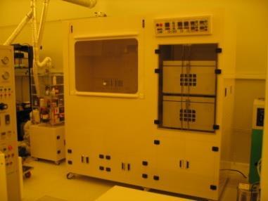
2 About KIMM Nano-research Bldg Clean RM Five Research Divisions; 1. Advanced Manufacturing Sys. 2. Extreme Mechanical Eng. 3. Nano-Convergence Mechanical Systems 4. Environmental and Energy Sys. 5. Mechanical Systems Safety 2
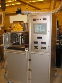
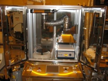
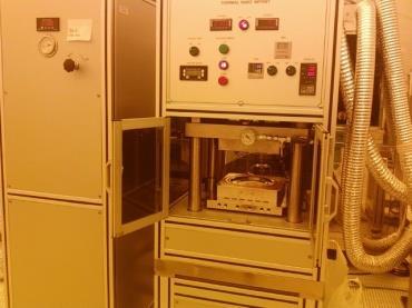
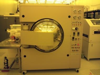
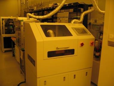
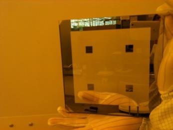
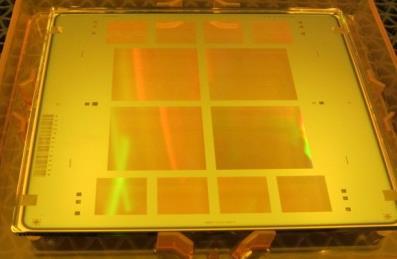
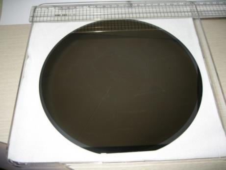
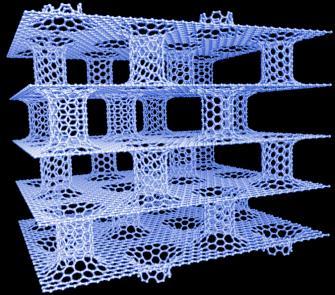
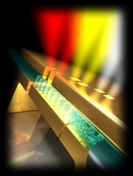
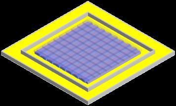
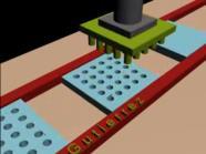
3 Facilities/Infra. For Nanoimprint at wafer scale For Nanoimprint in Large area Master/Molds Large area Mold fabrication Etched master at 8 wafer 3/26


4 Metal patterning infrastructures Film Quality w.r.t. dep. rate Ag deposited By E-beam v.s. 5.0 A /S 0.5A /S Siliver Milling Test w.r.t. the variables of current, time, and tilting angle Target Sub. Tilting angle ~60 A Tilting angle ~0 Current 300 A Time 1min B 4/26


5 Outlines 1 Laboratory Introduction Members / Facility Researches for Nanoimprint 2 Fabrication strategies Introduction of various in-house self technologies Metal Imprint Transfer 3 Application to Optoelectronic Devices Photoluminescence Transparent electrode in Hybrid Cell Photovoltatics 4 Closing remarks

6


7 Lift-off for well-round shaped Metal dots Process Scheme GT-IJPEN /26


8 Metal direct etch, Nanoimprint CMOS imaging chip + Plasmonic nano filter array + nanoimprint process Front Illumination &Reflection White Light Source SiO2 Al filter Si-wafer 8/26


9 Embedded Ag nanopatterning 1. Bilayer Hybrid NIL -> Lift-off 2. Metal Imprint Transfer Point of the embedded configuration on multilayer optoelectronics Non-uniform current flow (Leakage current) Reduced efficiency Electric field/electron injection enhancement Electron transport effects Thermal decay, reduced life-time Charge recommbination in solar cells Thermal decay, reduced efficiency 9/26
 (b) (b)")
 Step (d) (e) J.")
 (a) Half pre-cure of the coated UV")

 Lift-off of")
10 1. Bilayer Hybrid NIL and following Lift-off Process Scheme (a) (b) (b) Thermal Resist UV Resist Step (c) (c) (d) Step (d) (e) J. Nanophotonics 2014 Patent Step (e) (a) Half pre-cure of the coated UV resist (c) Thermal Imprint, UV exposure while pressed -> Complete cure of UV resist (d) Ag deposition by E-beam evaporation (e) Lift-off of thermal resist on top layer 10/26

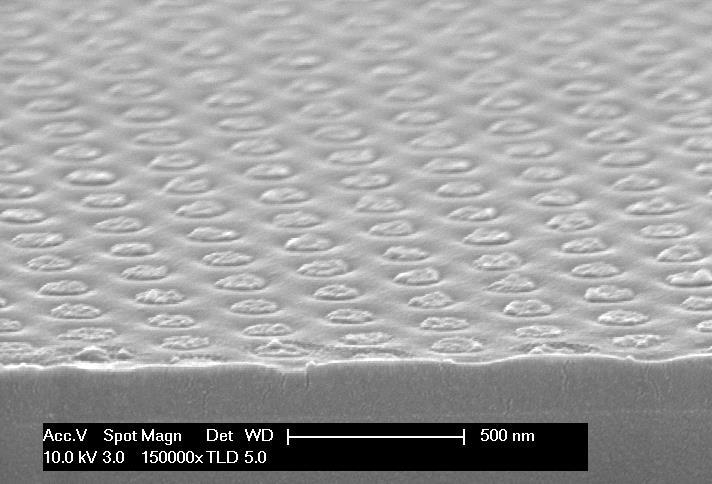
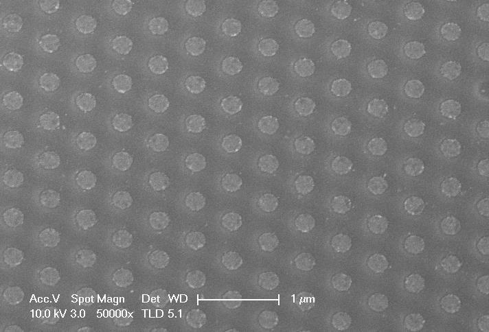
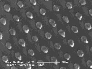
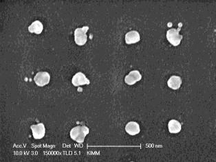
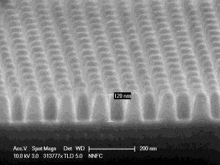
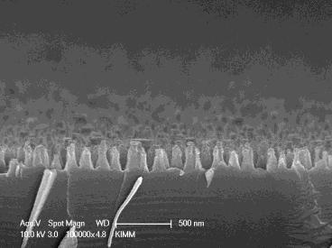
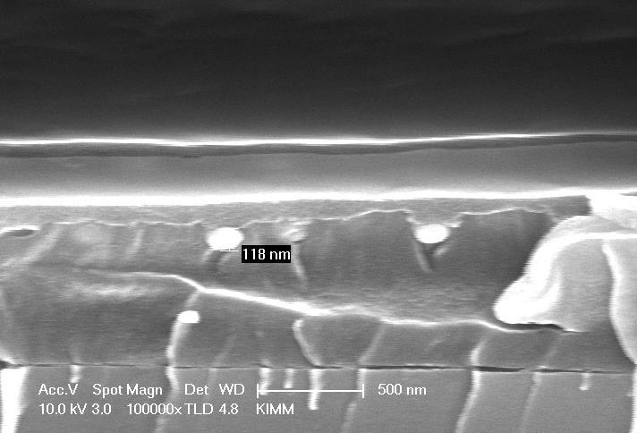
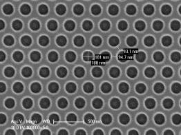
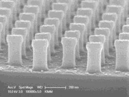
11 200nm Ag array (embedded) 150nm Ag array (embedded) 265nm Ag array (embedded) 235nm Ag array (embedded) 11/26
 E-beam evaporation of Ag on mold pattern (b) Half pre-cure of UV curable resist (c) Only Ag on the top surface of mold in contact")
 Half pre-cured UV-NIL resist 2) Limitedly")
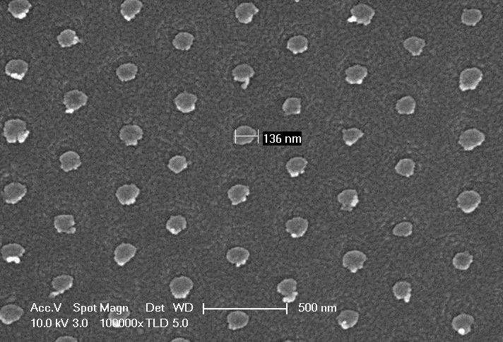
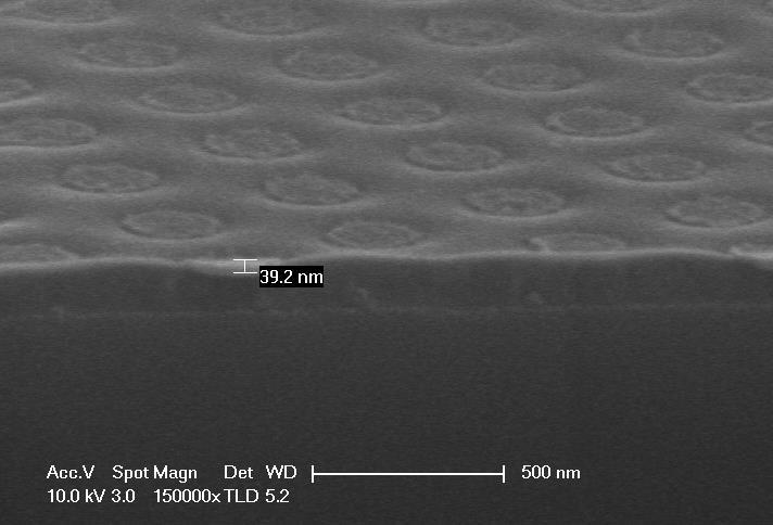
12 2. Metal Imprint Transfer (a) Process Scheme Ag E-beam Evaporation (c) (d) Mold release UV Exposure (b) UV curable resist Spin-coated Half pre-cured Qz substrate (a) E-beam evaporation of Ag on mold pattern (b) Half pre-cure of UV curable resist (c) Only Ag on the top surface of mold in contact with half-cured resist, and UV exposure (d) Mold release Kor. Patent: , US Patent: 14/ Small 2014, Published Note: Embedded Dot Arrays 1) Half pre-cured UV-NIL resist 2) Limitedly Imprinted Depth via Pressure Control 3) Minimized Leakage Current at device depo. 12/26
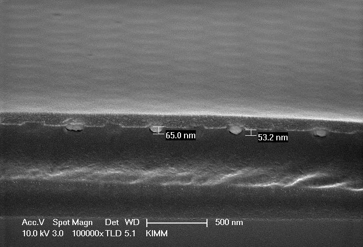
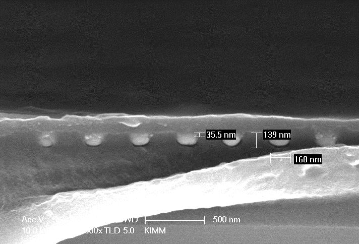
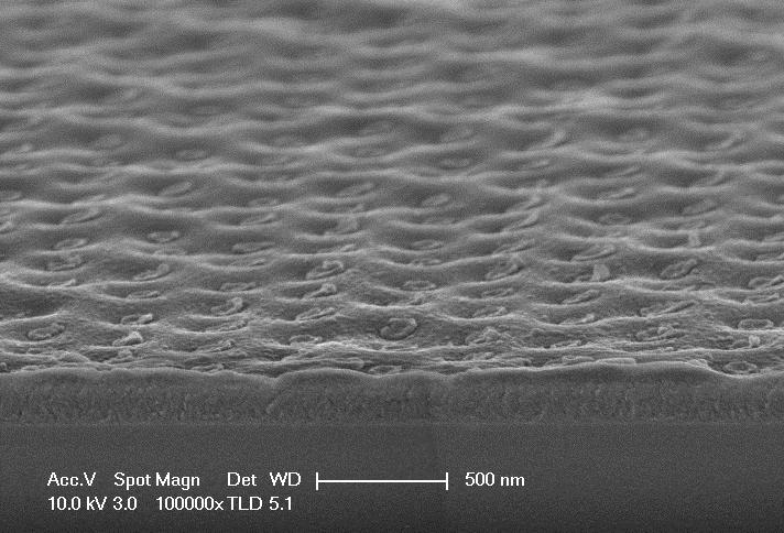
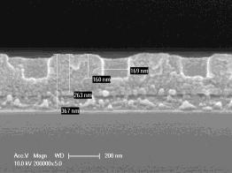
13 Completely embedded Planar embedded Half embedded 13/26

14

15 Metal Meshes in Hybrid Cell Process Scheme for Si-PEDOT Hybrid Photovoltaic cell 15/26


16 <Metal-based Meshes fabricated by Metal Imprint Transfer > T peak of 24 Ω/sq T peak of 16 Ω/sq T peak of 28 Ω/sq 16/26
17 17/26
18 Current density (ma/cm 2 ) Voc (V), Jsc (ma/cm 2 ) Au mesh (2 x 100 um) Au mesh (2 x 200 um) 5 Au mesh (2 x 300 um) 0 ITO Voltage (V) 2x100 2x200 2x300 ITO Au mesh size (um) Low shunt resistance PCE (%), FF (%) EQE (%) Au mesh (2x100 um) Au mesh (2x200 um) Au mesh (2x300 um) ITO Sample Wavelength (nm) V oc (mv) J sc (ma/cm 2 ) FF (%) PCE (%) ITO Au mesh (2x300 um) Au mesh (2x200 um) Au mesh (2x100 um) /26


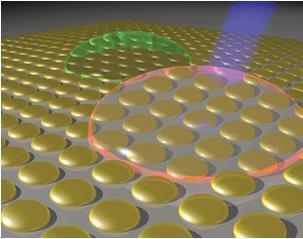
19 Tunable Plasmonic Nanostructures Metal Imprint Transfer Annealing at > 150 C Confirmed Tunable plasmonic Properties Plasmonic peak shifts as annealing temperature increases. Green PL Intensity increased more than 400%, w.r.t. Ref. 19/26
 Transmittance (%) 60 40 20 150nm 200nm 0 300 400 500 600 700 800 900 1000 Wavelength (nm) 265nm At 40nm, 250 (a)")
20 Spectral Transmittance- Measured & Simulated 100 Anneal Temp. dependence at 200nm 80 Transmittance (%) B-40-1 B-40-2 B-40-3 B C 200 C 150 C R.T A-40-4 B-40-4 C-40-4 Wavelength (nm) Transmittance (%) nm 200nm Wavelength (nm) 265nm At 40nm, 250 (a) cylinder shape 에서 ellipsoidal 로변하는과정의 transmittance (b)~(d) Electric field intensity of cylinder shape & ellipsoidal shape with a,b=80nm 20/26


21 Photoluminescence Improvements <Annealing Temp.-dependence> incident light PL peak intensity Mold pattern size: 150nm Ag Thick: 40nm Anneal temp.: R.T./150/200/250 C Ref.glass Ref.NOA A-40-1 A-40-2 A-40-3 A-40-4 Double-grating excitation monochromator Incident light 5 5 glass Sample compartment 320 mm spectrograph with double-grating turret A/B/C ; 150/200/265-nm in mold pattern dia. 20/40/60; 20/40/60-nm in Ag thickness 1/2/3/4; RT/150/200/250 C for annealing temp Wavelength(nm) PL enhancement rate Sample w.r.t Ref. glass w.r.t. Ref-NOA A % 317% A % 303% A % 293% A % 518% 21/26
22 <Ag Thick.-dependence> <Mold pattern size.-dependence> PL peak intensity Mold pattern size: 150nm Anneal temp.: 250 C Ag Thick: 20/40/60-nm Ref.glass Ref.NOA A-20-4 A-40-4 A-60-4 PL peak intensity Mold pattern size: 150/200/265-nm Anneal temp.: 250 C Ag Thick: 40-nm Ref.glass Ref.NOA A-40-4 B-40-4 C Wavelength(nm) PL enhancement rate Sample w.r.t Ref. glass w.r.t. Ref-NOA A % 276% A % 518% A % 446% Wavelength(nm) PL enhancement rate Sample w.r.t Ref. glass w.r.t. Ref-NOA A % 518% B % 415% C % 200% 22/26


23 Closing Remarks Research Infrastructures for Nanostructures/Patterning Nanoimprint-based nanopatterning and its application in Optoelectronics Several approaches for metallic nanopattern fabrications in plasmonic fields Global Collaborations UC Berkeley-Micromechanical Analysis and Design (BMAD) IMRE, Singapore AMO GmbH Aachen Industrial Collaborations APN Hutem Co. nanolambda Korea Company Samsung Electronics-Manufacturing Institute Youngchang Chemical Co. Ltd 23/26


24 Members Nanoimprint - Process, Tools, Functional mater. - Appl.: R-RAM, Sensors, (O)LED 3D Multiscale Architecturing - Nanowire structuring - Nanomaterials self-assembly Plasmonic sensors, Light emitting - Metal nanostructuring - Metal NP. Self-growth Staffs Lee, Eung-sug: Ultrafind fabrication, Nanomechatronics Jeong, Jun-ho: Nanolithography, Nanoimprint Choi, Jun-hyuk: Metal nanopattering, Direct/Roll Imprint Choi, Dae-geun: Nanoimprint mater. Process chemistry Lee, Ji-hye: Nanowire, mask fabrication, biosensors Jeong, Joo-yeon: Electronics, Plasmonic optics 24/26

25 Thank you for your attentions


26 Research area <Nanopatterning, Lithography> <Metal nanopattern array> <Optoelectronic Applications> <Etching> <Optics-based Sensors> <Metal pattern, Lift-off> <Plasmonic Lithography> 26


27 Research directions Multilayer, Enlarged Solar cells Planarized Struc. Plasmonic Litho. Mask Plasmonic sensors Undercut 3D Struc. Optoelectronics Embedded structure profile Infrastructure of metallic nanopatterning
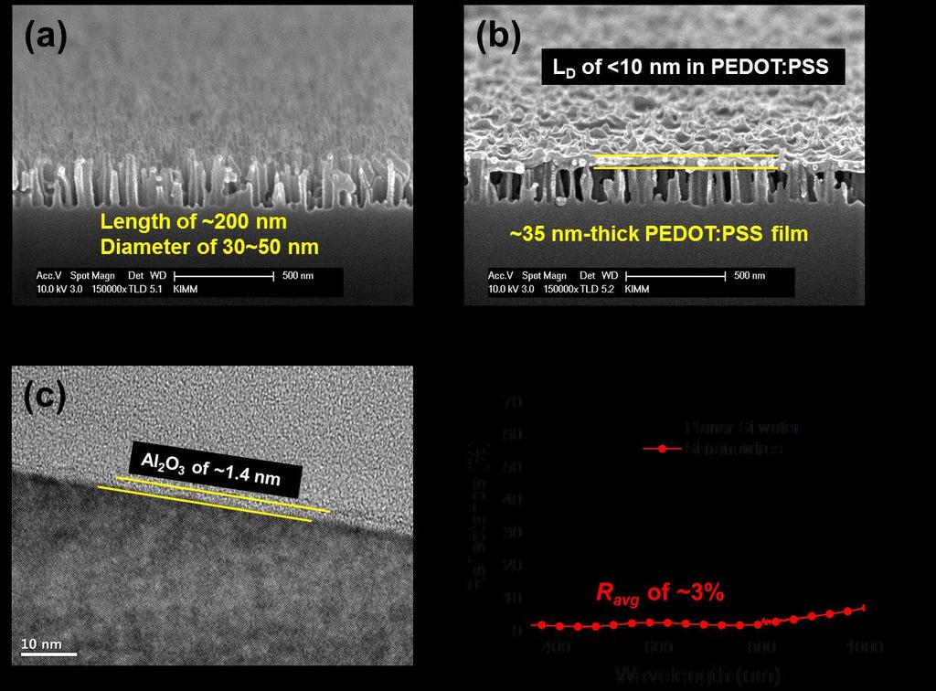
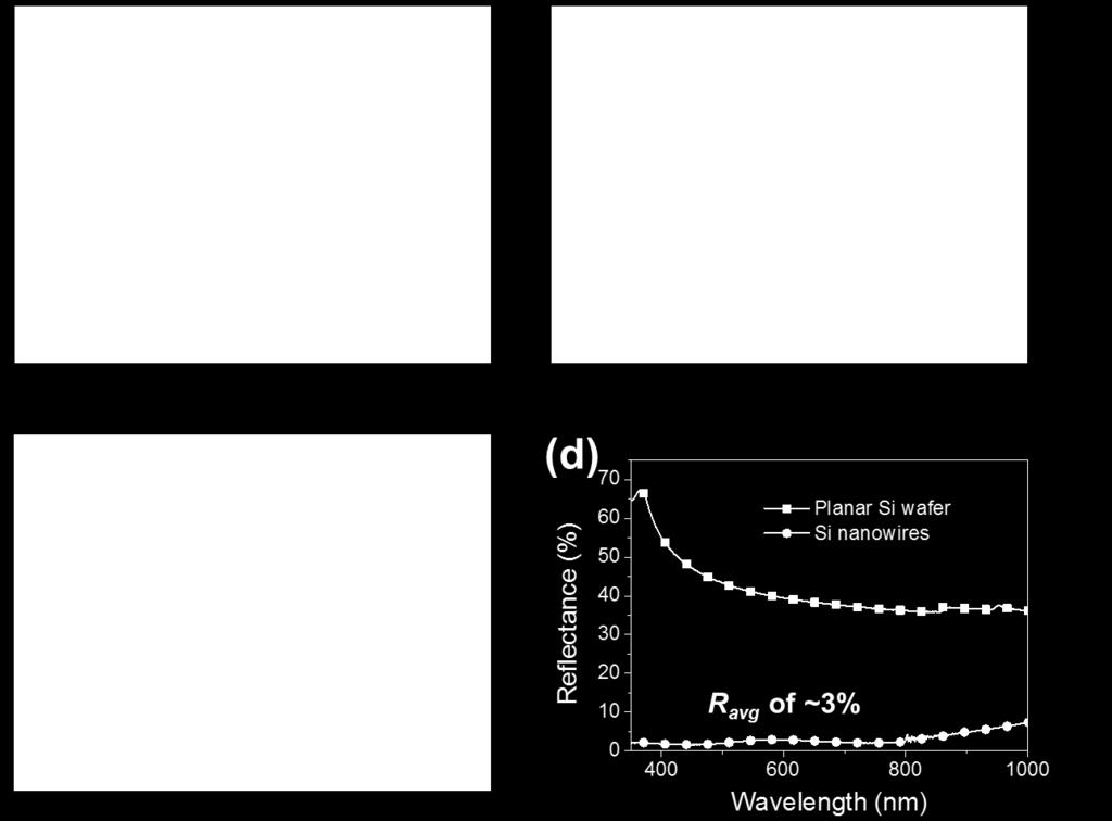
Towards scalable fabrication of high efficiency polymer solar cells
 Towards scalable fabrication of high efficiency polymer solar cells Hui Joon Park 2*, Myung-Gyu Kang 1**, Se Hyun Ahn 3, Moon Kyu Kang 1, and L. Jay Guo 1,2,3 1 Department of Electrical Engineering and
Nanoimprinting in Polymers and Applications in Cell Studies. Albert F. YEE Chemical Engineering & Materials Science UC Irvine
 Nanoimprinting in Polymers and Applications in Cell Studies Albert F. YEE Chemical Engineering & Materials Science UC Irvine Presentation outline Motivation Reversal imprinting Soft inkpad imprinting on
Nano-imprinting Lithography Technology І
 Nano-imprinting Lithography Technology І Agenda Limitation of photolithograph - Remind of photolithography technology - What is diffraction - Diffraction limit Concept of nano-imprinting lithography Basic
Metallic Antireflection Structures Made from Silver Ink by a Liquid Transfer Imprint Lithography Technique
 Journal of Photopolymer Science and Technology Volume 30, Number 5 (2017) 539-544 C 2017SPST Metallic Antireflection Structures Made from Silver Ink by a Liquid Transfer Imprint Lithography Technique Ichiro
Organic Solar Cells. Green River Project
 Organic Solar Cells Green River Project Silicon Cells Silicon semiconductors Advantages: Efficiencies Lifetimes Disadvantages: High manufacturing costs Inflexible http://en.wikipedia.org Organic semiconductors
SUPPLEMENTARY INFORMATION
 In the format provided by the authors and unedited. ARTICLE NUMBER: 16178 DOI: 10.1038/NENERGY.2016.178 Enhanced Stability and Efficiency in Hole-Transport Layer Free CsSnI3 Perovskite Photovoltaics Supplementary
Superionic Solid State Stamping (S4)
") Superionic Solid State Stamping (S4) Lead Faculty Researcher: Placid Ferreira Department: Materials Science & Engineering Hsu et al, Nano Letters, 2007 1. Description: This dry, single step, electrochemical
Superionic Solid State Stamping (S4) Lead Faculty Researcher: Placid Ferreira Department: Materials Science & Engineering Hsu et al, Nano Letters, 2007 1. Description: This dry, single step, electrochemical
Vertically aligned Ni magnetic nanowires fabricated by diblock-copolymer-directed Al thin film anodization
 Vertically aligned Ni magnetic nanowires fabricated by diblock-copolymer-directed Al thin film anodization Researcher: Kunbae (Kevin) Noh, Graduate Student, MAE Dept. and CMRR Collaborators: Leon Chen,
One-kilobit cross-bar molecular memory circuits at 30-nm half-pitch fabricated by nanoimprint lithography
 Appl. Phys. A 80, 1173 1178 (2005) DOI: 10.1007/s00339-004-3176-y Applied Physics A Materials Science & Processing w. wu 1, g.-y. jung 1 d.l. olynick 2 j. straznicky 1 z. li 1 x. li 1 d.a.a. ohlberg 1
Woven Electrodes for Optoelectronic Devices. Peter Chabrecek. Sefar AG, 9425 Thal, Switzerland
 Peter Chabrecek Sefar AG, 9425 Thal, Switzerland Actual SEFAR business Sefar's core skills is the manufacture and market of fabrics with precise mesh openings for screen printing and filtration processes
NanoSystemsEngineering: NanoNose Final Status, March 2011
 1 NanoSystemsEngineering: NanoNose Final Status, March 2011 The Nanonose project is based on four research projects (VCSELs, 3D nanolithography, coatings and system integration). Below, the major achievements
Multiphoton lithography based 3D micro/nano printing Dr Qin Hu
 Multiphoton lithography based 3D micro/nano printing Dr Qin Hu EPSRC Centre for Innovative Manufacturing in Additive Manufacturing University of Nottingham Multiphoton lithography Also known as direct
Micro & nanofabrica,on
 Micro & nanofabrica,on Photolitography : - contact - projec,on Electron Beam lithography (EBL) Nano imprint lithography Etching Contact Photolithography Substrate (e.g. Silicon wafer) Photoresist spinning
In-Situ Monitoring of Pattern Filling in Nano-Imprint Lithography Using Surface Plasmon Resonance
 Copyright 2011 American Scientific Publishers All rights reserved Printed in the United States of America Journal of Nanoscience and Nanotechnology Vol. 11, 1 6, 2011 In-Situ Monitoring of Pattern Filling
2. High Efficiency Crystalline Si Solar Cells
 2 High Efficiency Crystalline Si Solar Cells Students: Karthick Murukesan, Sandeep S S, Meenakshi Bhaisare, Bandana Singha, Kalaivani S and Ketan Warikoo Faculty members: Anil Kottantharayil, B M Arora,
New generation of solar cell technologies
 New generation of solar cell technologies Emerging technologies and their impact on the society 9th March 2017 Dhayalan Velauthapillai Professor, Faculty of Engineering and Business Administration Campus
Soft Lithography. Jin-Goo Park. Materials and Chemical Engineering Hanyang University, Ansan. Electronic Materials and Processing Lab.
 Hanyang University Soft Lithography Jin-Goo Park Materials and Chemical Engineering Hanyang University, Ansan Electronic Materials and Processing Lab. Introduction to Soft Lithography Research Micro- Electro-
Integration of Block-Copolymer with Nano- Imprint Lithography: Pushing the Boundaries of Emerging Nano-Patterning Technology
 Integration of Block-Copolymer with Nano- Imprint Lithography: Pushing the Boundaries of Emerging Nano-Patterning Technology April 2010 update SNL Geoff Brennecka (PI) Bruce Burckel Matt George Jack Skinner
Lecture 5. SOI Micromachining. SOI MUMPs. SOI Micromachining. Silicon-on-Insulator Microstructures. Agenda:
 EEL6935 Advanced MEMS (Spring 2005) Instructor: Dr. Huikai Xie SOI Micromachining Agenda: SOI Micromachining SOI MUMPs Multi-level structures Lecture 5 Silicon-on-Insulator Microstructures Single-crystal
Plasmonic Nanostructures II
 Plasmonic Nanostructures II Dr. Krüger / Prof. M. Zacharias, IMTEK, Propagation of SPPs Propagation distance decreases with decreasing strip width! 2 Dr. Krüger / Prof. M. Zacharias, IMTEK, Bound and leaky
TSV Processing and Wafer Stacking. Kathy Cook and Maggie Zoberbier, 3D Business Development
 TSV Processing and Wafer Stacking Kathy Cook and Maggie Zoberbier, 3D Business Development Outline Why 3D Integration? TSV Process Variations Lithography Process Results Stacking Technology Wafer Bonding
Reclaimed Silicon Solar Cells
 61 Reclaimed Silicon Solar Cells Victor Prajapati. Department ofmicroelectronic Engineering, 82 Lomb Memorial Dr., Rochester, NY 14623. Email: Victor.Prajapati@gmail.com Abstract Fully processed CMOS Si
Invited paper. Issues on nanoimprint lithography with a single-layer resist structure. Applied Physics A Materials Science & Processing
 Appl. Phys. A 81, 1331 1335 (2005) DOI: 10.1007/s00339-005-3313-2 g.y. jung 1 w. wu 1 s. ganapathiappan 1 d.a.a. ohlberg 1 m. saif islam 2 x. li 1 d.l. olynick 3 h. lee 4 y. chen 5 s.y. wang 1 w.m. tong
Processing guidelines
 Processing guidelines mr-uvcur21 series UV-curable Polymer for UV-based Nanoimprint Lithography Characteristics mr-uvcur21 is a liquid UV-curable polymer system with low viscosity and high curing rate
纳米压印技术最新进展. Obducat Technologies AB., Sweden Gang Luo,
 纳米压印技术最新进展 Obducat Technologies AB., Sweden Gang Luo, 20170711 History 2016 Launch of SINDRE Large Area 2015 Acquire Solarsemi Gmbh 2015 Awarded by NNT for Pioneering NIL into production 2014 Launch and
DEVELOPMENT OF HIGH EFFICIENCY FLEXIBLE CdTe SOLAR CELLS
 DEVELOPMENT OF HIGH EFFICIENCY FLEXIBLE CdTe SOLAR CELLS A.Romeo, M. Arnold, D.L. Bätzner, H. Zogg and A.N. Tiwari* Thin Films Physics Group, Laboratory for Solid State Physics, Swiss Federal Institute
ZnO-based Transparent Conductive Oxide Thin Films
 IEEE EDS Mini-colloquium WIMNACT 32 ZnO-based Transparent Conductive Oxide Thin Films Weijie SONG Ningbo Institute of Material Technology and Engineering, Chinese Academy of Sciences, Ningbo, P. R. China
Creating Greater Capacity on Smaller Spaces. Nanofabrication and Its Impact on Sensor Manufacturing
 Creating Greater Capacity on Smaller Spaces Nanofabrication and Its Impact on Sensor Manufacturing 2017-09-08 The context of Smart City and IoT Artifical Intelligence drivning the need for new smart devices
350 C for 8 hours in argon atmosphere. Supplementary Figures. Supplementary Figure 1 High-temperature annealing of BP flakes on SiO 2.
 Supplementary Figures Supplementary Figure 1 High-temperature annealing of BP flakes on SiO 2. (a-d) The optical images of three BP flakes on a SiO 2 substrate before (a,b) and after annealing (c,d) at
Introduction to Micro/Nano Fabrication Techniques. Date: 2015/05/22 Dr. Yi-Chung Tung. Fabrication of Nanomaterials
 Introduction to Micro/Nano Fabrication Techniques Date: 2015/05/22 Dr. Yi-Chung Tung Fabrication of Nanomaterials Top-Down Approach Begin with bulk materials that are reduced into nanoscale materials Ex:
Positive Photoresists
 Positive Photoresists Gesellschaft für chemische Materialien spezieller Photoresistsysteme mbh Positive Photoresists map 1200 series Thick resists map 1275, map 1275 HV Unique features of the positive
Light Trapping Enhancement in Thin Film Silicon Solar Cell with Different Back Reflector
 International Journal of Electrical Components and Energy Conversion 2017; 3(5): 83-87 http://www.sciencepublishinggroup.com/j/ijecec doi: 10.11648/j.ijecec.20170305.11 ISSN: 2469-8040 (Print); ISSN: 2469-8059
Large-area patterning by roller-based nanoimprint lithography
 JOANNEUM RESEARCH Forschungsgesellschaft Institute MATERIALS, Weiz, Austria Large-area patterning by roller-based nanoimprint lithography Ursula Palfinger, Dieter Nees, Stephan Ruttloff, Markus Leitgeb,
Bistable nano-structured photoalignment surface by nanoimprint lithography
 Bistable nano-structured photoalignment surface by nanoimprint lithography Chung-Yung Lee (SID Member) Man-Chun Tseng (SID Student Member) Jacob Yeuk-Lung Ho (SID Member) Vladimir G. Chigrinov (SID Fellow)
Light enhancement by the formation of an Al-oxide honeycomb nano-structure on the n-gan surface of thin-gan light-emitting diodes
 Light enhancement by the formation of an Al-oxide honeycomb nano-structure on the n-gan surface of thin-gan light-emitting diodes C. L. Lin, P. H. Chen Department of Chemical and Materials Engineering,
IMRE/ETPL Flagship Project
 IMRE/ETPL Flagship Project Nanoparticulate Barrier Films & Gas Permeation Measurement Techniques for Thin Film Solar & Display Application Problems Senthil Ramadas Institute of Materials Research & Engineering
Step and Flash Imprint Lithography for sub-100nm Patterning
 Step and Flash Imprint Lithography for sub-100nm Patterning Matthew Colburn, Annette Grot, Marie Amistoso, Byung Jin Choi, Todd Bailey, John Ekerdt, S.V. Sreenivasan, James Hollenhorst, C. Grant Willson
TSV Interposer Process Flow with IME 300mm Facilities
 TSV Interposer Process Flow with IME 300mm Facilities Property of Institute of Microelectronics (IME)-Singapore August 17, 2012 Outline 1. TSV interposer (TSI) cross sectional schematic TSI with BEOL,
Dr. Priyabrat Dash Office: BM-406, Mob: Webpage: MB: 205
 Email: dashp@nitrkl.ac.in Office: BM-406, Mob: 8895121141 Webpage: http://homepage.usask.ca/~prd822/ MB: 205 Nonmanufacturing In continuation from last class... 2 Top-Down methods Mechanical-energy methods
Synergetic plasmonic effect of Al and Au nanoparticles for efficiency. enhancement of air processed organic photovoltaic devices
 Electronic Electronic Supplementary Information Synergetic plasmonic effect of Al and Au nanoparticles for efficiency enhancement of air processed organic photovoltaic devices George Kakavelakis a,b, Emmanuel
Correlating the scattered intensities of P3HT and PCBM to the current. densities of polymer solar cells
 Supplementary Information for Correlating the scattered intensities of P3HT and PCBM to the current densities of polymer solar cells Enrique D. Gomez*, Katherine P. Barteau, He Wang, Michael F. Toney,
White Paper: Pixelligent Internal Light Extraction Layer for OLED Lighting
 White Paper: Pixelligent Internal Light Zhiyun (Gene) Chen, Ph.D., Vice President of Engineering Jian Wang, Ph.D., Manager, Application Engineering Pixelligent Technologies LLC, 6411 Beckley Street, Baltimore,
Large Area Functional Surfaces By Roll-to-Roll Nanoimprint Lithography Project: APPOLO
 Large Area Functional Surfaces By Roll-to-Roll Nanoimprint Lithography Project: APPOLO Mr. Theodoros Tachtsidis Nanotypos 23rd and 24th of June Amsterdam Core Overview Nanotypos is a pioneering research
A New Architecture for Transparent Electrodes: Relieving the Trade-Off Between Electrical Conductivity and Optical Transmittance
 A New Architecture for Transparent Electrodes: Relieving the Trade-Off Between Electrical Conductivity and Optical Transmittance Ping Kuang, Joong-Mok Park, Wai Leung, Rakesh C. Mahadevapuram, Kanwar S.
Fabrication Technologies and Instruments. The available fabrication technologies and instruments for fabricating the sub-wavelength
 Chapter 3 Fabrication Technologies and Instruments 3.1 Introduction The available fabrication technologies and instruments for fabricating the sub-wavelength grating will be described in this chapter.
EXCIMER LASER ANNEALING FOR LOW- TEMPERATURE POLYSILICON THIN FILM TRANSISTOR FABRICATION ON PLASTIC SUBSTRATES
 EXCIMER LASER ANNEALING FOR LOW- TEMPERATURE POLYSILICON THIN FILM TRANSISTOR FABRICATION ON PLASTIC SUBSTRATES G. Fortunato, A. Pecora, L. Maiolo, M. Cuscunà, D. Simeone, A. Minotti, and L. Mariucci CNR-IMM,
Barix Multilayers: a Water and Oxygen Barrier for Flexible Organic Electronics. Robert Jan Visser
 Barix Multilayers: a Water and Oxygen Barrier for Flexible Organic Electronics Robert Jan Visser Organic Electronics Is the Future of Electronics Organic? MIT Stanford UC Berkeley Nano Forum Vitex Systems,
CREOL, The College of Optics & Photonics, University of Central Florida
 Metal Substrate Induced Control of Ag Nanoparticle Plasmon Resonances for Tunable SERS Substrates Pieter G. Kik 1, Amitabh Ghoshal 1, Manuel Marquez 2 and Min Hu 1 1 CREOL, The College of Optics and Photonics,
Photoresist Coat, Expose and Develop Laboratory Dr. Lynn Fuller
 ROCHESTER INSTITUTE OF TECHNOLOGY MICROELECTRONIC ENGINEERING Photoresist Coat, Expose and Develop Laboratory Dr. Lynn Fuller Webpage: http://www.rit.edu/lffeee 82 Lomb Memorial Drive Rochester, NY 14623-5604
R&D ACTIVITIES AT ASSCP-BHEL,GURGAON IN SOLAR PV. DST-EPSRC Workshop on Solar Energy Research
 R&D ACTIVITIES AT -BHEL,GURGAON IN SOLAR PV at the DST-EPSRC Workshop on Solar Energy Research (22 nd 23 rd April, 2009) by Dr.R.K. Bhogra, Addl. General Manager & Head Email: cpdrkb@bhel.co.in Dr.A.K.
Polymer-based optical interconnects using nano-imprint lithography
 Polymer-based optical interconnects using nano-imprint lithography Arjen Boersma,Sjoukje Wiegersma Bert Jan Offrein, Jeroen Duis, Jos Delis, Markus Ortsiefer, Geert van Steenberge, MikkoKarppinen, Alfons
High-efficiency GaN-based light-emitting diodes fabricated with identical Ag contact formed on both n- and p-layers
 High-efficiency GaN-based light-emitting diodes fabricated with identical Ag contact formed on both n- and p-layers Munsik Oh and Hyunsoo Kim * School of Semiconductor and Chemical Engineering and Semiconductor
Optical Control of Surface Plasmon Coupling in Organic Light Emitting Devices with Nanosized Multi-cathode Structure
 Proceedings of the 5 th International Conference on Nanotechnology: Fundamentals and Applications Prague, Czech Republic, August 11-13, 2014 Paper No. 234 Optical Control of Coupling in Organic Light Emitting
Lecture 19 Microfabrication 4/1/03 Prof. Andy Neureuther
 EECS 40 Spring 2003 Lecture 19 Microfabrication 4/1/03 Prof. ndy Neureuther How are Integrated Circuits made? Silicon wafers Oxide formation by growth or deposition Other films Pattern transfer by lithography
Amorphous Oxide Transistor Electrokinetic Reflective Display on Flexible Glass
 Amorphous Oxide Transistor Electrokinetic Reflective Display on Flexible Glass Devin A. Mourey, Randy L. Hoffman, Sean M. Garner *, Arliena Holm, Brad Benson, Gregg Combs, James E. Abbott, Xinghua Li*,
Inline-high-rate thermal evaporation of aluminum for novel industrial solar cell metallization
 2nd Workshop on Metallization Konstanz, April 14 th -15 th, 2010 Inline-high-rate thermal evaporation of aluminum for novel industrial solar cell metallization Frank Heinemeyer 1 Motivation Development
Nanofabrication Prof. Stephen Y. Chou NanoStructure Laboratory
 Nanofabrication Prof. Stephen Y. Chou Department of Electrical Engineering Princeton University 1 Acknowledgment Dr. Paul Fischer Dr. Yun Wang Dr. Jay Guo Dr. Peter Klauss Dr. Jim Wang Dr. Longtin He Dr.
Nonplanar Metallization. Planar Metallization. Professor N Cheung, U.C. Berkeley
 Nonplanar Metallization Planar Metallization Passivation Metal 5 (copper) Metal 3 (copper) Interlevel dielectric (ILD) Via (tungsten) Metal 1 (copper) Tungsten Plug to Si Silicon Caps and Plugs oxide oxide
Surface Preparation and Cleaning Conference April 19-20, 2016, Santa Clara, CA, USA. Nano-Bio Electronic Materials and Processing Lab.
 Surface Preparation and Cleaning Conference April 19-20, 2016, Santa Clara, CA, USA Issues on contaminants on EUV mask Particle removal on EUV mask surface Carbon contamination removal on EUV mask surface
200mm Next Generation MEMS Technology update. Florent Ducrot
 200mm Next Generation MEMS Technology update Florent Ducrot The Most Exciting Industries on Earth Semiconductor Display Solar 20,000,000x reduction in COST PER TRANSISTOR in 30 years 1 20x reduction in
HIGH-THROUGHPUT, CONTINUOUS NANOPATTERNING TECHNOLOGIES FOR DISPLAY AND ENERGY APPLICATIONS
 HIGH-THROUGHPUT, CONTINUOUS NANOPATTERNING TECHNOLOGIES FOR DISPLAY AND ENERGY APPLICATIONS by Se Hyun Ahn A dissertation submitted in partial fulfillment of the requirements for the degree of Doctor of
Investigation of metal contacts via thermal treatment at Interfaces between low temperature Ag pastes and TCO layer for HIT solar cell
 Investigation of metal contacts via thermal treatment at Interfaces between low temperature Ag pastes and TCO layer for HIT solar cell Ming-Shiou Lin, Kuang-Yang Kuo, Yong-Han Lin, Yueh-Lin Lee, Liang-Pin
Fabrication of sawtooth diffraction gratings using nanoimprint lithography
 Fabrication of sawtooth diffraction gratings using nanoimprint lithography Chih-Hao Chang, a) R. K. Heilmann, R. C. Fleming, J. Carter, E. Murphy, and M. L. Schattenburg Massachusetts Institute of Technology,
PARAMETER EFFECTS FOR THE GROWTH OF THIN POROUS ANODIC ALUMINUM OXIDES
 10.1149/1.2794473, The Electrochemical Society PARAMETER EFFECTS FOR THE GROWTH OF THIN POROUS ANODIC ALUMINUM OXIDES S. Yim a, C. Bonhôte b, J. Lille b, and T. Wu b a Dept. of Chem. and Mat. Engr., San
Challenges for Commercially viable Transparent Conductive Oxide Layers
 Challenges for Commercially viable Transparent Conductive Oxide Layers Arkema Inc. 900 First Ave., King of Prussia, PA 19406 R. Y. Korotkov, L. Fang, P. Ricou, M. Bluhm, J. Coffey, C. Polsz and G. Silverman
Nanophotonics: principle and application. Khai Q. Le Lecture 11 Optical biosensors
 Nanophotonics: principle and application Khai Q. Le Lecture 11 Optical biosensors Outline Biosensors: Introduction Optical Biosensors Label-Free Biosensor: Ringresonator Theory Measurements: Bulk sensing
Nano-Scale Manufacturing:
 The Second U.S.-Korea Forum on Nanotechnology: Nanomanufacturing Research and Education Nano-Scale Manufacturing: Top-down, Bottom-up and System Engineering Cheng Sun, Xiang Zhang Center of Scalable and
Sputtered Zinc Oxide Films for Silicon Thin Film Solar Cells: Material Properties and Surface Texture
 Poster FVS Workshop 2002 Sputtered Zinc Oxide Films for Silicon Thin Film Solar Cells: Material Properties and Surface Texture Texture etching of sputtered ZnO:Al films has opened up a variety of possibilities
Formation of and Light Emission from Si nanocrystals Embedded in Amorphous Silicon Oxides
 10.1149/1.2392914, copyright The Electrochemical Society Formation of and Light Emission from Si nanocrystals Embedded in Amorphous Silicon Oxides D. Comedi a, O. H. Y. Zalloum b, D. E. Blakie b, J. Wojcik
Fabrication Of Metallic Antenna Arrays Using Nanoimprint Lithography
 University of Central Florida Electronic Theses and Dissertations Masters Thesis (Open Access) Fabrication Of Metallic Antenna Arrays Using Nanoimprint Lithography 2013 Yu-Wei Lin University of Central
THIN FILM THICKNESS MEASUREMENT FOR EVALUATION OF RESIDUAL LAYER OF NANO-IMPRINT LITHOGRAPHY USING NEAR-FIELD OPTICS
 9 th INTERNATIONAL SYMPOSIUM ON MEASUREMENT AND QUALITY CONTROL (9 th ISMQC) November 21 24, 27, IIT Madras THIN FILM THICKNESS MEASUREMENT FOR EVALUATION OF RESIDUAL LAYER OF NANO-IMPRINT LITHOGRAPHY
High-Speed Roll-to-Roll Nanoimprint Lithography on Flexible Plastic Substrates**
 COMMUNICATION DOI: 10.1002/adma.200702650 High-Speed Roll-to-Roll Nanoimprint Lithography on Flexible Plastic Substrates** By Se Hyun Ahn and L. Jay Guo* The ability of micro- to nanometer-scale patterning
NTT-AT Optical Adhesives Lineup. Adhesives / Resins and Sealants for Optical Component Assembly
 NTT-AT Optical Adhesives Lineup Adhesives / Resins and Sealants for Optical Component Assembly The adhesive technology used in optical communications is one of the key technologies we offer. Ask us anything
ISSN: ISO 9001:2008 Certified International Journal of Engineering and Innovative Technology (IJEIT) Volume 3, Issue 6, December 2013
 Volume 3, Issue 6, December 2013") ISSN: 2277-3754 Fabrication and Characterization of Flip-Chip Power Light Emitting Diode with Backside Reflector Ping-Yu Kuei, Wen-Yu Kuo, Liann-Be Chang, Tung-Wuu Huang, Ming-Jer Jeng, Chun-Te Wu, Sung-Cheng
ISSN: 2277-3754 Fabrication and Characterization of Flip-Chip Power Light Emitting Diode with Backside Reflector Ping-Yu Kuei, Wen-Yu Kuo, Liann-Be Chang, Tung-Wuu Huang, Ming-Jer Jeng, Chun-Te Wu, Sung-Cheng
A Novel Extrusion Microns Embossing Method of Polymer Film
 Modern Mechanical Engineering, 2012, 2, 35-40 http://dx.doi.org/10.4236/mme.2012.22005 Published Online May 2012 (http://www.scirp.org/journal/mme) A Novel Extrusion Microns Embossing Method of Polymer
LIFETIME CHARACTERIZATION AT IMEC
 LIFETIME CHARACTERIZATION AT IMEC IMEC ENERGY 1, ESZTER VOROSHAZI 1,2 1. imec, Organic Photovoltaics, Kapeldreef 75, Leuven (Belgium) 2. Katholieke Universiteit Leuven, ESAT, Kasteelpark Arenberg 10, Leuven
At wavelength characterization of EUV and soft X-ray gratings
 At wavelength characterization of EUV and soft X-ray gratings F. Scholze, A, Haase, C. Laubis, V. Soltwisch, J. Wernecke, M. Krumrey Physikalisch-Technische Bundesanstalt, Abbestraße 2-12, 10587 Berlin,
Mater. Res. Soc. Symp. Proc. Vol Materials Research Society
 Mater. Res. Soc. Symp. Proc. Vol. 940 2006 Materials Research Society 0940-P13-12 A Novel Fabrication Technique for Developing Metal Nanodroplet Arrays Christopher Edgar, Chad Johns, and M. Saif Islam
EE40 Lec 22. IC Fabrication Technology. Prof. Nathan Cheung 11/19/2009
 Suggested Reading EE40 Lec 22 IC Fabrication Technology Prof. Nathan Cheung 11/19/2009 300mm Fab Tour http://www-03.ibm.com/technology/manufacturing/technology_tour_300mm_foundry.html Overview of IC Technology
Hybrid III-V/Si DFB laser integration on a 200 mm fully CMOS-compatible silicon photonics platform
 Hybrid III-V/Si DFB laser integration on a 200 mm fully CMOS-compatible silicon photonics platform B. Szelag 1, K. Hassan 1, L. Adelmini 1, E. Ghegin 1,2, Ph. Rodriguez 1, S. Bensalem 1, F. Nemouchi 1,
ABSTRACT: INTRODUCTION:
 ABSTRACT: Nano-Composite Polymer Optical Coatings Tom Faris Vampire Optical Coatings, Inc. P.O. Box 240 Kirkersville, Ohio 43033 (740)-927-5257 f(740)-927-5032 vampirecoatings@earthlink.net Traditionally
Nanoimprint Lithography - Next Generation Nanopatterning Methods for Nanophotonics Fabrication
 14 Nanoimprint Lithography - Next Generation Nanopatterning Methods for Nanophotonics Fabrication Jukka Viheriälä, Tapio Niemi, Juha Kontio and Markus Pessa Optoelectronics Research Centre, Tampere University
Seminar Micro- and Nano-technology
 Seminar Micro- and Nano-technology Seminar 1 Schedule Wednesday 17:45-18:30 Yannick Bourgin yannick.bourgin@uni-jena.de Phone: +49(3641)947990 www.iap.uni-jena.de Presentations 2 Presentation by 2 students
MICROFABRICATION OF OPTICALLY ACTIVE InO X MICROSTRUCTURES BY ULTRASHORT LASER PULSES
 Journal of Optoelectronics and Advanced Materials Vol. 4, No. 3, September 2002, p. 809-812 MICROFABRICATION OF OPTICALLY ACTIVE InO X MICROSTRUCTURES BY ULTRASHORT LASER PULSES Foundation for Research
Thermochromic halide perovskite solar cells
 SUPPLEMENTARY INFORMATION Articles https://doi.org/10.1038/s41563-017-0006-0 In the format provided by the authors and unedited. Thermochromic halide perovskite solar cells Jia Lin 1,2,3, Minliang Lai
nanosilicon Nanophotonics
 nanosilicon Nanophotonics Lorenzo Pavesi Universita di Trento Italy Outline Silicon Photonics NanoSilicon photonics Silicon Nanophotonics NanoSilicon Nanophotonics Conclusion Outline Silicon Photonics
High-Resolution, Electrohydrodynamic Inkjet Printing of Stretchable, Metal Oxide Semiconductor Transistors with High Performances
 Electronic Supplementary Material (ESI) for Nanoscale. This journal is The Royal Society of Chemistry 2016 ` Electronic Supplementary Information High-Resolution, Electrohydrodynamic Inkjet Printing of
Advanced Sheet-to-Sheet and Roll-to-Roll thin-film processing on ultra-thin flexible glass for flexible electronic devices
 Advanced Sheet-to-Sheet and Roll-to-Roll thin-film processing on ultra-thin flexible glass for flexible electronic devices M. Junghaehnel 1, J. Westphalen 1, F. Naumann 2, G. Lorenz 2, M. Fahland 1, S.
FABRICATION PROCESSES FOR MAGNETIC MICROACTUATORS WITH POLYSILICON FLEXURES. Jack W. Judy and Richard S. Muller
 FABRICATION PROCESSES FOR MAGNETIC MICROACTUATORS WITH POLYSILICON FLEXURES Jack W. Judy and Richard S. Muller Berkeley Sensor & Actuator Center (BSAC) Department of EECS, University of California, Berkeley,
Recrystallization in CdTe/CdS
 Thin Solid Films 361±362 (2000) 420±425 www.elsevier.com/locate/tsf Recrystallization in CdTe/CdS A. Romeo, D.L. BaÈtzner, H. Zogg, A.N. Tiwari* Thin Film Physics Group, Institute of Quantum Electronics,
Plating on Thin Conductive Oxides for Silicon Heterojunction Solar Cells
 Plating on Thin Conductive Oxides for Silicon Heterojunction Solar Cells A. Lachowicz 1, A. Faes 1, P. Papet 2, J. Geissbühler 3,J. Levrat 1, C. Allebé 1, N. Badel 1, J. Champliaud 1, F. Debrot 1, J. Cattin
Passivation of Porous Silicon by LaF 3 Using a Simple Single-Source Chemical Bath Technique
 International Journal of Materials and Chemistry 2012, 2(3): 111-115 DOI: 10.5923/j.ijmc.20120203.05 Passivation of Porous Silicon by LaF 3 Using a Simple Abdul Al Mortuza 1, Md. Hafizur Rahman 2, Sinthia
Free standing Multilayer Thin Film of Cellulose Nanocrystals
 Free standing Multilayer Thin Film of Cellulose Nanocrystals Chaoyang Jiang Department of Chemistry The University of South Dakota Edmonton, June 25, 2009 Cellulose Nanocrystals Nanotechnology R&D Priority
Photonic Drying Pulsed Light as a low Temperature Sintering Process
 Photonic Drying Pulsed Light as a low Temperature Sintering Process Lou Panico Xenon Corporation W E S T E R N M I C H I G A N U N I V E R S I T Y PRESENTATION OVERVIEW What is Printed Electronics Materials
Process steps for Field Emitter devices built on Silicon wafers And 3D Photovoltaics on Silicon wafers
 Process steps for Field Emitter devices built on Silicon wafers And 3D Photovoltaics on Silicon wafers David W. Stollberg, Ph.D., P.E. Research Engineer and Adjunct Faculty GTRI_B-1 Field Emitters GTRI_B-2
Optimization of optical performances in submicron silicon-on-insulator rib and strip waveguides by H 2 thermal annealing
 I N S T I T U T D E R E C H E R C H E T E C H N O L O G I Q U E Optimization of optical performances in submicron silicon-on-insulator rib and strip waveguides by H thermal annealing Erwine Pargon 1, Cyril
Presented at the 28th European PV Solar Energy Conference and Exhibition, 30 September 4 October, 2013, Paris, France
 INTEGRATING DIFFRACTIVE REAR SIDE STRUCTURES FOR LIGHT TRAPPING INTO CRYSTALLINE SILICON SOLAR CELLS J. Eisenlohr 1*, H. Hauser 1, J. Benick 1, A. Mellor 2, B. Bläsi 1, J.C. Goldschmidt 1, M. Hermle 1
Challenges for Embedded Device Technologies for Package Level Integration
 Challenges for Embedded Device Technologies for Package Level Integration Kevin Cannon, Steve Riches Tribus-D Ltd Guangbin Dou, Andrew Holmes Imperial College London Embedded Die Technology IMAPS-UK/NMI
A Uniform Pressure Apparatus for Micro/Nanoimprint Lithography Equipment
 Paper: A Uniform Pressure Apparatus for Micro/Nanoimprint Lithography Equipment Jian-Shian Lin Λ;ΛΛ, Chieh-Lung Lai Λ, Ya-Chun Tu Λ, Cheng-Hua Wu Λ, and Yoshimi Takeuchi ΛΛ Λ Mechanical and System Research