Motorola MPA1016FN FPGA
|
|
|
- Ernest Jones
- 5 years ago
- Views:
Transcription
1 Construction Analysis Motorola MPA1016FN FPGA Report Number: SCA Global Semiconductor Industry the Serving Since N. Hartford Drive Scottsdale, AZ Phone: Fax: Internet:
2 INDEX TO TEXT TITLE PAGE INTRODUCTION 1 MAJOR FINDINGS 1 TECHNOLOGY DESCRIPTION Assembly 2 Die Process 2-3 ANALYSIS RESULTS I Assembly 4 ANALYSIS RESULTS II Die Process and Design 5-6 ANALYSIS PROCEDURE 7 TABLES Overall Evaluation 8 Package Markings 9 Wirebond Strength 9 Die Material Analysis 9 Horizontal Dimensions 10 Vertical Dimensions 11 - i -
3 INTRODUCTION This report describes a construction analysis of the Motorola MPA1016FN FPGA. Two devices packaged in 84-pin Plastic Leaded Chip Carriers (PLCCs) and five scribed dice were received for the analysis. These devices were fabricated by Chartered Semiconductor Manufacturing. The packaged devices were date coded MAJOR FINDINGS Questionable Items: 1 None. Special Features: Three levels of reflowed ( hot ) aluminum. 1 These items present possible quality or reliability concerns. They should be discussed with the manufacturer to determine their possible impact on the intended application
4 TECHNOLOGY DESCRIPTION Assembly: The devices were encapsulated in 84-pin Plastic Leaded Chip Carriers (PLCCs). The copper (Cu) leadframe was internally spot-plated with silver (Ag). External pins were tinned with tin-lead (SnPb) solder. Lead-locking provisions (anchors) at all pins. Thermosonic ball bonding using 1.2 mil O.D. gold wire. Sawn dicing (full-depth). Silver-filled epoxy die attach. Die Process: Fabrication process: Selective oxidation CMOS process employing twin-wells in a P-substrate. Final passivation: A layer of nitride over a layer of glass. Metallization: Three levels of metal defined by standard dry-etch techniques. Metal 3 and metal 2 consisted of aluminum with a titanium-nitride (TiN) cap and titanium (Ti) barrier. Metal 1 consisted of aluminum with a titanium-nitride cap and a titanium-nitride/titanium barrier. All three levels of aluminum were reflowed to fill contacts/vias ( hot aluminum ). Standard vias and contacts were used (no plugs)
5 TECHNOLOGY DESCRIPTION (continued) Interlevel dielectrics: Interlevel dielectrics consisted of two layers of silicon-dioxide with a planarizing spin-on-glass (SOG) between them. The SOG had been etched back. Polysilicon: A single layer of polycide (poly cap over titanium silicide on poly) was used to form all gates on the die. Definition was by a dry etch of normal quality. Direct poly-to-diffusion (buried) contacts were not used. Diffusions: Implanted N+ and P+ diffusions formed the sources/drains of the CMOS transistors. An LDD process was used with oxide sidewall spacers left in place. Wells: Twin-wells in a P-substrate. A step was present at well boundaries. Redundancy: Fuses were not used. Memory cells: Programming is achieved through a modified 6T CMOS SRAM cell. Metal 3 was used to form the bit lines (via metal 2 and metal 1). Metal 2 was used to distribute Vcc and GND (via metal 1). Metal 1 was used to provide cell interconnect. Polycide was used to form all gates and word lines
6 ANALYSIS RESULTS I Assembly : Figures 1-3 Questionable Items: None. General Items: The devices were encapsulated in 84-pin Plastic Leaded Chip Carriers (PLCCs). Overall package quality: Good. Internal spot-plating of the copper leadframe was silver. External pins were tinned with tin-lead (SnPb). No cracks or voids present. No gaps were noted at lead exits. Lead-locking provisions (anchors) were present at all pins. Wirebonding: Thermosonic ballbond method using 1.2 mil O.D. gold wire. No bond lifts occurred during wirepull tests and bond pull strengths were good. Die attach: Silver-filled epoxy of normal quality. No voids were noted in the die attach and no problems are foreseen. Die dicing: Die separation was by sawing (full depth) with normal quality workmanship
7 ANALYSIS RESULTS II Die Process and Design : Figures 4-33 Questionable Items: 1 None. Special Features: Three levels of reflowed ( hot ) aluminum. General items: Fabrication process: Devices were fabricated using selective oxidation CMOS process employing twin-wells in a P-substrate. Process implementation: Die layout was clean and efficient. Alignment was good at all levels. No damage or contamination was found. Die coat: No die coat was present. Final passivation: A layer of nitride over a layer of glass. Integrity tests indicated defect-free passivation. Edge seal was good as the passivation extended beyond the metal at the edge of the die. Metallization: Three levels of metal defined by standard dry-etch techniques. Metal 3 and metal 2 consisted of aluminum with a titanium-nitride (TiN) cap and titanium (Ti) barrier. Metal 1 consisted of aluminum with a titanium-nitride cap and a titanium-nitride/titanium barrier. All three levels of aluminum were reflowed to provide excellent step coverage. Standard vias and contacts were used (no plugs). Metal patterning: All metal levels were patterned by a dry etch of normal quality. Metal defects: No voiding, notching, or neckdown was noted in any of the metal layers. No silicon nodules were noted following removal of the metal layers. 1 These items present possible quality or reliability concerns. They should be discussed with the manufacturer to determine their possible impact on the intended application
8 ANALYSIS RESULTS II (continued) Metal step coverage: All three levels of aluminum were reflowed to provide excellent step coverage. No metal thinning occurred at any vias or contacts. Interlevel dielectrics: Interlevel dielectrics consisted of two layers of silicon-dioxide with a planarizing spin-on-glass (SOG) between them. The SOG had been etched back. Pre-metal dielectric: A layer of reflow glass (BPSG) over densified oxide was used under metal 1. Reflow was performed prior to contact cuts only. Contact defects: Contact and via cuts were defined by a two-step process. No over-etching of contacts was noted, but significant overetch was present at vias. This is not a problem in this case since the overetched aluminum is filled by the aluminum that fills the via. No problems were found. Polysilicon: A single layer of polycide (poly cap over titanium silicide on poly) was used to form all gates on the die. Definition was by a dry-etch of normal quality. Direct poly-to-diffusion (buried) contacts were not used. Diffusions: Standard implanted N+ and P+ diffusions formed the sources/drains of the CMOS transistors. An LDD process was used with oxide sidewall spacers left in place. No problems were found. Isolation: LOCOS (local oxide isolation). A step was present at the well boundaries, confirming the presence of twin-wells. Redundancy: Fuses were not present on the die. Memory cells: Programming is achieved through a modified 6T CMOS SRAM cell. Metal 3 was used to form the bit lines (via metal 2 and metal 1). Metal 2 was used to distribute Vcc and GND (via metal 1). Metal 1 was used to provide cell interconnect. Polycide was used to form all gates and word lines
9 PROCEDURE The devices were subjected to the following analysis procedures: External inspection X-ray Decapsulate Internal optical inspection SEM of assembly features and passivation Wirepull test Passivation integrity test Passivation removal SEM inspection of metal 3 Delayer to metal 2 and inspect Delayer to metal 1 and inspect Metal 1 removal and inspect barrier Delayer to silicon and inspect poly/die surface Die sectioning (90 for SEM) * Die material analysis Measure horizontal dimensions Measure vertical dimensions * Delineation of cross-sections is by silicon etch unless otherwise indicated
10 OVERALL QUALITY EVALUATION : Overall Rating: Good DETAIL OF EVALUATION Package integrity Package markings Die placement Die attach quality Wire spacing Wirebond placement Wirebond quality Dicing quality Wirebond method Die attach method Dicing method G N N G G G N G Thermosonic ball bond method using 1.2 mil O.D. gold wire. Silver-epoxy Sawn (full depth) Die surface integrity: Tool marks (absence) Particles (absence) Contamination (absence) Process defects General workmanship Passivation integrity Metal definition Metal integrity Metal registration Contact coverage Contact registration G G G G N G N G G G G G = Good, P = Poor, N = Normal, NP = Normal/Poor - 8 -
11 PACKAGE MARKINGS TOP (LOGO) MPA1016FN ZQUAL9640 WIREBOND STRENGTH Wire material: Die pad material: Material at package lands: 1.2 mil O.D. gold aluminum silver Sample # 1 # of wires tested: 20 Bond lifts: 0 Force to break - high: 15.0g - low: 11.0g - avg.: 13.0g - std. dev.: 0.3 DIE MATERIAL ANALYSIS Final passivation: Metallization 3: Metallization 2: Metallization 1: Polycide: A layer of silicon-nitride over a layer of glass. Aluminum (Al) with a titanium-nitride (TiN) cap and titanium (Ti) barrier. Aluminum (Al) with a titanium-nitride (TiN) cap and titanium (Ti) barrier. Aluminum (Al) with a titanium-nitride (TiN) cap and titanium-nitride/titanium barrier. Polysilicon cap over Titanium (Ti) silicide on poly
12 HORIZONTAL DIMENSIONS Die size: 6.1 x 6.2 mm (241 x 245 mils) Die area: 38 mm 2 (59,045 mils 2 ) Min pad size: Min pad window: Min pad space: Min metal 3 width: Min metal 3 space: Min metal 3 pitch: Min metal 2 width: Min metal 2 space: Min metal 2 pitch: Min metal 1 width: Min metal 1 space: Min metal 1 pitch: Min via (M3-to-M2): Min via (M2-to-M1): Min contact: Min polycide width: Min polycide space: Min gate length * - (N-channel): 0.1 x 0.1 mm (3.9 x 4.0 mils) 0.09 x 0.09 mm (3.5 x 3.6 mils) 0.04 mm (1.4 mils) 1.0 micron 1.2 micron 2.2 microns 0.9 micron 1.2 micron 2.1 microns 0.6 micron 0.8 micron 1.5 micron 0.6 micron (round) 0.6 micron (round) 0.8 micron (round) 0.5 micron 1.0 micron 0.5 micron - (P-channel): 0.5 micron * Physical gate length
13 VERTICAL DIMENSIONS Die thickness: 0.5 mm (19 mils) Layers Passivation 2: Passivation 1: 0.6 micron 0.4 micron Metal 3 - cap: 0.05 micron (approx.) - aluminum: 0.8 micron - barrier: 0.12 micron Intermetal dielectric 2 - glass 2: 0.4 micron (average) - SOG: micron - glass 1: 0.4 micron (average) Metal 2 - cap: 0.05 micron (approx.) - aluminum: 0.5 micron - barrier: 0.1 micron Intermetal dielectric 1 - glass 2: 0.4 micron (average) - SOG: micron - glass 1: 0.4 micron (average) Metal 1 - cap: 0.05 micron (approx.) - aluminum: 0.5 micron - TiN/ Ti barrier: 0.17 micron Pre-metal glass: Poly - poly cap: 0.4 micron (avg.) 0.02 micron (approx.) - silicide: 0.15 micron - poly: 0.2 micron Local oxide: 0.4 micron N+ S/D diffusion: 0.25 micron P+ S/D diffusion: 0.25 micron N-well: 2.5 microns (approx.)
14 INDEX TO FIGURES ASSEMBLY Figures 1-3 DIE LAYOUT AND IDENTIFICATION Figures 4-6 PHYSICAL DIE STRUCTURES Figures 7-26 COLOR DRAWING OF DIE STRUCTURE Figure 27 MEMORY CELL STRUCTURES Figures CIRCUIT LAYOUT AND I/O Figures ii -


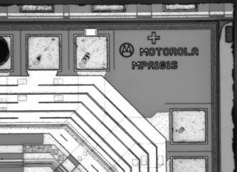
15 PIN 1 Figure 1. Package photograph and x-ray of the Motorola MPA1016FN FPGA. Mag. 2.3x.


16 DIE PADDLE Mag. 150x EDGE OF PASSIVATION Mag. 1000x Figure 2. SEM views illustrating dicing and edge seal. 60.


17 EDGE OF PASSIVATION DIE Mag. 810x METAL 3 EDGE OF PASSIVATION METAL 1 N+ Mag. 5000x Figure 3. SEM section views of the edge seal.

18 Figure 4. Whole die photograph of the Motorola MPA1016FN FPGA. Mag. 26x.


19 Figure 5. Optical views of die markings. Mag. 300x.


20 Figure 6. Optical views of die corners. Mag. 170x.


21 PASSIVATION 2 METAL 3 SOG METAL 1 POLYCIDE GATE N+ S/D LOCOS PASSIVATION 2 METAL 3 METAL 2 SOG METAL 1 LOCOS POLYCIDE glass etch Figure 7. SEM section views illustrating general structure. Mag. 6500x


22 METAL 2 POLYCIDE METAL 1 METAL 2 METAL 1 S/D POLYCIDE Figure 8. Perspective SEM views illustrating general structure. Mag. 10,000x, 60.


23 Mag. 3,200x Mag. 13,000x Figure 9. SEM views illustrating final passivation. 60.


24 PASSIVATION 2 PASSIVATION 1 METAL 3 ILD 2 Mag. 26,000x TiN CAP ALUMINUM 3 Ti BARRIER Mag. 52,000x Figure 10. SEM section views of metal 3 line profiles.


25 METAL 3 VIAS Figure 11. Topological SEM views of metal 3 patterning. Mag. 3200x, 0.


26 Mag. 4200x Mag. 4200x TiN CAP Mag. 26,000x ALUMINUM 3 Figure 12. Perspective SEM views of metal 3 step coverage. 60.


27 METAL 3 ILD 2 Mag. 26,000x SOG METAL 2 Ti BARRIER ALUMINUM 3 Mag. 52,000x TiN CAP ALUMINUM 2 Ti BARRIER GLASS 2 SOG GLASS 1 Mag. 52,000x METAL 2 Figure 13. SEM section views illustrating a typical M3-to-M2 via and interlevel dielectric 2 composition.


28 ILD 2 METAL 2 SOG ILD 1 METAL 1 Mag. 26,000x TiN CAP SOG ALUMINUM 2 Ti BARRIER Mag. 52,000x Figure 14. SEM section views of metal 2 line profiles.


29 METAL 2 Mag. 3200x Mag. 3200x Mag. 6500x Figure 15. Topological SEM views of metal 2 patterning. 0.


30 Mag. 5000x Mag. 5000x TiN CAP Mag. 30,000x ALUMINUM 2 Figure 16. Perspective SEM views of metal 2 step coverage. 60.


31 METAL 2 ILD 1 Mag. 26,000x METAL 1 SOG Ti BARRIER ALUMINUM 2 Mag. 52,000x ALUMINUM 1 TiN CAP TiN BARRIER GLASS 2 GLASS 1 SOG Mag. 52,000x METAL 1 Figure 17. SEM section views illustrating a typical M2-to-M1 via and interlevel dielectric 1 composition.


32 METAL 2 METAL 1 SOG POLYCIDE LOCOS Mag. 26,000x TiN CAP ALUMINUM 1 SOG TiN BARRIER Ti ADHESION LAYER Mag. 52,000x Figure 18. SEM section views of metal 1 line profiles.


33 VIA POLYCIDE METAL 1 CONTACTS Mag. 3200x Mag. 3200x Mag. 5000x Figure 19. Topological SEM views of metal 1 patterning. 0.


34 Mag. 5000x Mag. 5000x TiN CAP POLYCIDE Mag. 25,000x ALUMINUM 1 TiN BARRIER Figure 20. Perspective SEM views of metal 1 step coverage. 60.


35 METAL 1 SOG PRE-METAL DIELECTRIC POLYCIDE LOCOS SOG METAL 1 N+ SOG POLYCIDE GATE METAL 1 P+ S/D Figure 21. SEM section views of typical metal 1 contacts. Mag. 26,000x.


36 Figure 22. Topological SEM views of polycide patterning. Mag. 3200x, 0.


37 N+ Mag. 5700x P+ P+ Mag. 5700x N+ POLYCIDE GATE Mag. 26,000x LOCOS S/D Figure 23. Perspective SEM views of polycide coverage. 60.


38 POLYCIDE GATE N-channel N+ S/D N+ S/D GATE OXIDE POLYCIDE GATE REFLOW GLASS P-channel P+ S/D P+ S/D POLY CAP PRE-METAL DIELECTRIC SIDEWALL SPACER W SILICIDE POLY glass etch Figure 24. SEM section views of typical transistors. Mag. 52,000x.


39 POLYCIDE LOCOS GATE OXIDE REFLOW GLASS N+ LOCOS N+ Figure 25. SEM section views illustrating a typical birdsbeak and local oxide isolation. Mag. 52,000x.


40 N-WELL DELINEATION ARTIFACTS P SUBSTRATE Mag. 1500x METAL 1 SOG P+ S/D LOCOS N-WELL STEP AT WELL BOUNDARY Mag. 13,000x Figure 26. Section views illustrating well structure.
41 POLY CAP TiN CAP TiN BARRIER Ti ADHESION LAYER METAL 3 PASSIVATION 2 PASSIVATION 1 W SILICIDE POLY Motorola MPA1016FN ILD 2 METAL 2 ILD 1 METAL 1 PRE-METAL DIELECTRIC,,,,,,,,, N+ S/D P-WELL LOCOS,,,,,,,,, P SUBSTRATE P+ S/D N-WELL Orange = Nitride, Blue = Metal, Yellow = Oxide, Green = Poly, Red = Diffusion, and Gray = Substrate Figure 27. Color cross section drawing illustrating device structure.


42 metal 3 metal 2 Figure 28. Topological SEM views of the FPGA array area. Mag. 810x.


43 metal 1 unlayered Figure 29. Topological SEM views of the FPGA array area. Mag. 810x.


44 BIT metal 3 BIT GND V CC metal 2 Figure 30. Topological SEM views of the FPGA Base 6T-SRAM cell. Mag. 3200x.


45 BIT GND GND metal 1 V CC V CC WORD A WORD B 1 BIT unlayered 4 6 WORD A WORD B BIT Figure 31. Topological SEM views and schematic of the FPGA Base 6T-SRAM cell. Mag. 3200x.


46 Mag. 1000x Mag. 400x Figure 32. Optical views of typical circuitry and input protection.

47 PASSIVATION 2 METAL 3 SOG METAL 1 ILD1 ILD2 METAL 2 POLYCIDE GATE P+ S/D N+ GUARDBAND STEP AT WELL BOUNDRY Figure 33. SEM section view of the I/O circuitry. Mag. 6500x.
Rockwell R RF to IF Down Converter
 Construction Analysis Rockwell R6732-13 RF to IF Down Converter Report Number: SCA 9709-552 Global Semiconductor Industry the Serving Since 1964 17350 N. Hartford Drive Scottsdale, AZ 85255 Phone: 602-515-9780
NKK NR4645LQF Bit RISC Microprocessor
 Construction Analysis NKK NR4645LQF-133 64-Bit RISC Microprocessor Report Number: SCA 9707-547 Global Semiconductor Industry the Serving Since 1964 17350 N. Hartford Drive Scottsdale, AZ 85255 Phone: 602-515-9870
Lattice isplsi1032e CPLD
 Construction Analysis Lattice isplsi1032e CPLD Report Number: SCA 9612-522 Global Semiconductor Industry the Serving Since 1964 15022 N. 75th Street Scottsdale, AZ 85260-2476 Phone: 602-998-9780 Fax: 602-948-1925
Mosel Vitelic MS62256CLL-70PC 256Kbit SRAM
 Construction Analysis Mosel Vitelic MS62256CLL-70PC 256Kbit SRAM Report Number: SCA 9703-499 Global Semiconductor Industry the Serving Since 1964 17350 N. Hartford Drive Scottsdale, AZ 85255 Phone: 602-515-9780
Oki M A-60J 16Mbit DRAM (EDO)
") Construction Analysis Oki M5117805A-60J 16Mbit DRAM (EDO) Report Number: SCA 9707-545 Global Semiconductor Industry the Serving Since 1964 17350 N. Hartford Drive Scottsdale, AZ 85255 Phone: 602-515-9780
Construction Analysis Oki M5117805A-60J 16Mbit DRAM (EDO) Report Number: SCA 9707-545 Global Semiconductor Industry the Serving Since 1964 17350 N. Hartford Drive Scottsdale, AZ 85255 Phone: 602-515-9780
UMC UM F-7 2M-Bit SRAM
 Construction Analysis UMC UM 613264F-7 2M-Bit SRAM Report Number: SCA 9609-511 Global Semiconductor Industry the Serving Since 1964 15022 N. 75th Street Scottsdale, AZ 85260-2476 Phone: 602-998-9780 Fax:
Motorola MC68360EM25VC Communication Controller
 Construction Analysis EM25VC Communication Controller Report Number: SCA 9711-562 Global Semiconductor Industry the Serving Since 1964 17350 N. Hartford Drive Scottsdale, AZ 85255 Phone: 602-515-9780 Fax:
Dallas Semicoductor DS80C320 Microcontroller
 Construction Analysis Dallas Semicoductor DS80C320 Microcontroller Report Number: SCA 9702-525 Global Semiconductor Industry the Serving Since 1964 15022 N. 75th Street Scottsdale, AZ 85260-2476 Phone:
Analog Devices ADSP KS-160 SHARC Digital Signal Processor
 Construction Analysis Analog Devices ADSP-21062-KS-160 SHARC Digital Signal Processor Report Number: SCA 9712-575 Global Semiconductor Industry the Serving Since 1964 17350 N. Hartford Drive Scottsdale,
SGS-Thomson M28C K EEPROM
 Construction Analysis SGS-Thomson M28C64-121 64K EEPROM Report Number: SCA 9710-559 Global Semiconductor Industry the Serving Since 1964 17350 N. Hartford Drive Scottsdale, AZ 85255 Phone: 602-515-9780
NEC 79VR5000 RISC Microprocessor
 Construction Analysis NEC 79VR5000 RISC Microprocessor Report Number: SCA 9711-567 Global Semiconductor Industry the Serving Since 1964 17350 N. Hartford Drive Scottsdale, AZ 85255 Phone: 602-515-9780
Xilinx XC4036XL-1C FPGA
 Construction Analysis Xilinx XC4036XL-1C FPGA Report Number: SCA 9709-553 Global Semiconductor Industry the Serving Since 1964 17350 N. Hartford Drive Scottsdale, AZ 85255 Phone: 602-515-9780 Fax: 602-515-9781
Lattice 3256A-90LM PLD
 Construction Analysis PLD Report Number: SCA 9705-538 Global Semiconductor Industry the Serving Since 1964 17350 N. Hartford Drive Scottsdale, AZ 85255 Phone: 602-515-9780 Fax: 602-515-9781 e-mail: ice@ice-corp.com
Maximum MAX662 12V DC-DC Converter
 Construction Analysis Maximum MAX662 12V DC-DC Converter Report Number: SCA 9512-445 Global Semiconductor Industry the Serving Since 1964 17350 N. Hartford Drive Scottsdale, AZ 85255 Phone: 602-515-9780
Micron Semiconductor MT5C64K16A1DJ 64K x 16 SRAM
 Construction Analysis Micron Semiconductor MT5C64K16A1DJ 64K x 16 SRAM Report Number: SCA 9412-394 Global Semiconductor Industry the Serving Since 1964 17350 N. Hartford Drive Scottsdale, AZ 85255 Phone:
DEC SA-110S StrongARM 32-Bit Microprocessor
 Construction Analysis DEC SA-110S StrongARM 32-Bit Microprocessor Report Number: SCA 9704-535 Global Semiconductor Industry the Serving Since 1964 15022 N. 75th Street Scottsdale, AZ 85260-2476 Phone:
Xilinx XC4036EX FPGA
 Construction Analysis Xilinx XC4036EX FPGA Report Number: SCA 9706-544 Global Semiconductor Industry the Serving Since 1964 15022 N. 75th Street Scottsdale, AZ 85260-2476 Phone: 602-998-9780 Fax: 602-948-1925
Hitachi A 64Mbit (8Mb x 8) Dynamic RAM
 Dynamic RAM") Construction Analysis Hitachi 5165805A 64Mbit (8Mb x 8) Dynamic RAM Report Number: SCA 9712-565 Global Semiconductor Industry the Serving Since 1964 17350 N. Hartford Drive Scottsdale, AZ 85255 Phone:
Construction Analysis Hitachi 5165805A 64Mbit (8Mb x 8) Dynamic RAM Report Number: SCA 9712-565 Global Semiconductor Industry the Serving Since 1964 17350 N. Hartford Drive Scottsdale, AZ 85255 Phone:
Micron Semiconductor MT4LC16M4H9 64Mbit DRAM
 Construction Analysis Micron Semiconductor MT4LC16M4H9 64Mbit DRAM Report Number: SCA 9705-539 Global Semiconductor Industry the Serving Since 1964 15022 N. 75th Street Scottsdale, AZ 85260-2476 Phone:
SGS-Thomson L4990 Controller
 Construction Analysis SGS-Thomson L4990 Controller Report Number: SCA 9710-560 Global Semiconductor Industry the Serving Since 1964 17350 N. Hartford Drive Scottsdale, AZ 85255 Phone: 602-515-9780 Fax:
SGS-Thomson M17C1001 1Mb UVEPROM
 Construction Analysis SGS-Thomson M17C1001 1Mb UVEPROM Report Number: SCA 9612-518 Global Semiconductor Industry the Serving Since 1964 15022 N. 75th Street Scottsdale, AZ 85260-2476 Phone: 602-998-9780
Altera EPM7128SQC EPLD
 Construction Analysis Altera EPM7128SQC160-15 EPLD Report Number: SCA 9712-569 Global Semiconductor Industry the Serving Since 1964 17350 N. Hartford Drive Scottsdale, AZ 85255 Phone: 602-515-9780 Fax:
National Semiconductor LM2672 Simple Switcher Voltage Regulator
 Construction Analysis National Semiconductor LM2672 Simple Switcher Voltage Regulator Report Number: SCA 9712-570 Global Semiconductor Industry the Serving Since 1964 17350 N. Hartford Drive Scottsdale,
Motorola PC603R Microprocessor
 Construction Analysis Motorola PC603R Microprocessor Report Number: SCA 9709-551 Global Semiconductor Industry the Serving Since 1964 17350 N. Hartford Drive Scottsdale, AZ 85255 Phone: 602-515-9780 Fax:
Intel Pentium Processor W/MMX
 Construction Analysis Intel Pentium Processor W/MMX Report Number: SCA 9706-540 Global Semiconductor Industry the Serving Since 1964 15022 N. 75th Street Scottsdale, AZ 85260-2476 Phone: 602-998-9780 Fax:
VTC VM365830VSJ Pre-Amp
 Construction Analysis VTC VM365830VSJ Pre-Amp Report Number: SCA 9708-549 Global Semiconductor Industry the Serving Since 1964 17350 N. Hartford Drive Scottsdale, AZ 85255 Phone: 602-515-9780 Fax: 602-515-9781
Integrated Circuit Engineering Corporation. DRAMs
 DRAMs As generally known, the focus of technology in this product category continues to be complex vertical polysilicon structures to reduce cell area. This not only pushes the limits of deposition and
Integrated Circuit Engineering Corporation EPROM
 EPROM There was lots of discussion and many technical papers covering the promises of EPROM (typically Flash) at the IEDM conference last December, but here as in the other memory areas, not much in the
Renesas M5M40R326 32Mbit DRAM Memory Structural Analysis
 August 13, 2004 Renesas M5M40R326 32Mbit DRAM Memory Structural Analysis For questions, comments, or more information about this report, or for any additional technical needs concerning semiconductor technology,
Chapter 4 : ULSI Process Integration (0.18 m CMOS Process)
") Chapter : ULSI Process Integration (0.8 m CMOS Process) Reference. Semiconductor Manufacturing Technology : Michael Quirk and Julian Serda (00). - (00). Semiconductor Physics and Devices- Basic Principles(/e)
Chapter : ULSI Process Integration (0.8 m CMOS Process) Reference. Semiconductor Manufacturing Technology : Michael Quirk and Julian Serda (00). - (00). Semiconductor Physics and Devices- Basic Principles(/e)
9/4/2008 GMU, ECE 680 Physical VLSI Design
 ECE680: Physical VLSI Design Chapter II CMOS Manufacturing Process 1 Dual-Well Trench-Isolated CMOS Process gate-oxide TiSi 2 AlCu Tungsten SiO 2 p-well poly n-well SiO 2 n+ p-epi p+ p+ 2 Schematic Layout
Chapter 2 Manufacturing Process
 Digital Integrated Circuits A Design Perspective Chapter 2 Manufacturing Process 1 CMOS Process 2 CMOS Process (n-well) Both NMOS and PMOS must be built in the same silicon material. PMOS in n-well NMOS
Lecture 030 Integrated Circuit Technology - I (5/8/03) Page 030-1
 Page 030-1") Lecture 030 Integrated Circuit Technology - I (5/8/03) Page 030-1 LECTURE 030 INTEGRATED CIRCUIT TECHNOLOGY - I (References [7,8]) Objective The objective of this presentation is: 1.) Illustrate integrated
Lecture 030 Integrated Circuit Technology - I (5/8/03) Page 030-1 LECTURE 030 INTEGRATED CIRCUIT TECHNOLOGY - I (References [7,8]) Objective The objective of this presentation is: 1.) Illustrate integrated
CMOS Technology. Flow varies with process types & company. Start with substrate selection. N-Well CMOS Twin-Well CMOS STI
 CMOS Technology Flow varies with process types & company N-Well CMOS Twin-Well CMOS STI Start with substrate selection Type: n or p Doping level, resistivity Orientation, 100, or 101, etc Other parameters
Manufacturing Process
 Digital Integrated Circuits A Design Perspective Jan M. Rabaey Anantha Chandrakasan Borivoje Nikolic Manufacturing Process July 30, 2002 1 CMOS Process 2 A Modern CMOS Process gate-oxide TiSi 2 AlCu Tungsten
EE BACKEND TECHNOLOGY - Chapter 11. Introduction
 1 EE 212 FALL 1999-00 BACKEND TECHNOLOGY - Chapter 11 Introduction Backend technology: fabrication of interconnects and the dielectrics that electrically and physically separate them. Aluminum N+ Early
ECE 659. Jan M. Rabaey Anantha Chandrakasan Borivoje Nikolic. July 30, Digital EE141 Integrated Circuits 2nd Manufacturing.
 Digital Integrated Circuits A Design Perspective Jan M. Rabaey Anantha Chandrakasan Borivoje Nikolic Manufacturing Process July 0, 00 1 CMOS Process 1 A Modern CMOS Process gate-oxide TiSi AlCu Tungsten
ECE520 VLSI Design. Lecture 7: CMOS Manufacturing Process. Payman Zarkesh-Ha
 ECE520 VLSI Design Lecture 7: CMOS Manufacturing Process Payman Zarkesh-Ha Office: ECE Bldg. 230B Office hours: Wednesday 2:00-3:00PM or by appointment E-mail: pzarkesh@unm.edu Slide: 1 Review of Last
ECE321 Electronics I
 ECE321 Electronics I Lecture 19: CMOS Fabrication Payman Zarkesh-Ha Office: ECE Bldg. 230B Office hours: Tuesday 2:00-3:00PM or by appointment E-mail: payman@ece.unm.edu Slide: 1 Miller Effect Interconnect
Manufacturing Process
 CMOS Manufacturing Process CMOS Process 1 A Modern CMOS Process gate-oxide TiSi AlCu Tungsten SiO n+ p-well p-epi poly n-well p+ SiO p+ Dual-Well Trench-Isolated CMOS Process Circuit Under Design V DD
10 Manor Parkway, Suite C Salem, New Hampshire
 Micro-Precision Technologies (MPT) is an independent manufacturer of hybrid integrated circuits, multichip modules, and high-precision thick film substrates for the military, medical, avionics, optoelectronics,
CMOS Manufacturing Process
 CMOS Manufacturing Process CMOS Process A Modern CMOS Process gate-oxide TiSi 2 AlCu Tungsten SiO 2 n+ p-well p-epi poly n-well p+ SiO 2 p+ Dual-Well Trench-Isolated CMOS Process Circuit Under Design V
1 Thin-film applications to microelectronic technology
 1 Thin-film applications to microelectronic technology 1.1 Introduction Layered thin-film structures are used in microelectronic, opto-electronic, flat panel display, and electronic packaging technologies.
Semiconductor Manufacturing Technology. IC Fabrication Process Overview
 Semiconductor Manufacturing Technology Michael Quirk & Julian Serda October 00 by Prentice Hall Chapter 9 IC Fabrication Process Overview /4 Objectives After studying the material in this chapter, you
Silicon Wafer Processing PAKAGING AND TEST
 Silicon Wafer Processing PAKAGING AND TEST Parametrical test using test structures regularly distributed in the wafer Wafer die test marking defective dies dies separation die fixing (not marked as defective)
CMOS Manufacturing process. Design rule set
 CMOS Manufacturing process Circuit design Set of optical masks Fabrication process Circuit designer Design rule set Process engineer All material: Chap. 2 of J. Rabaey, A. Chandrakasan, B. Nikolic, Digital
Chapter 3 Silicon Device Fabrication Technology
 Chapter 3 Silicon Device Fabrication Technology Over 10 15 transistors (or 100,000 for every person in the world) are manufactured every year. VLSI (Very Large Scale Integration) ULSI (Ultra Large Scale
VLSI Design and Simulation
 VLSI Design and Simulation CMOS Processing Technology Topics CMOS Processing Technology Semiconductor Processing How do we make a transistor? Fabrication Process Wafer Processing Silicon single crystal
Lecture 200 BiCMOS Technology (12/12/01) Page 200-1
 Page 200-1") Lecture 200 BiCMOS Technology (12/12/01) Page 200-1 LECTURE 200 BICMOS TECHNOLOGY (READING: Text-Sec. 2.11) INTRODUCTION Objective Illustrate BiCMOS technology Outline Introduction Physical process illustration
Lecture 200 BiCMOS Technology (12/12/01) Page 200-1 LECTURE 200 BICMOS TECHNOLOGY (READING: Text-Sec. 2.11) INTRODUCTION Objective Illustrate BiCMOS technology Outline Introduction Physical process illustration
Chapter 4 Fabrication Process of Silicon Carrier and. Gold-Gold Thermocompression Bonding
 Chapter 4 Fabrication Process of Silicon Carrier and Gold-Gold Thermocompression Bonding 4.1 Introduction As mentioned in chapter 2, the MEMs carrier is designed to integrate the micro-machined inductor
CMOS FABRICATION. n WELL PROCESS
 CMOS FABRICATION n WELL PROCESS Step 1: Si Substrate Start with p- type substrate p substrate Step 2: Oxidation Exposing to high-purity oxygen and hydrogen at approx. 1000 o C in oxidation furnace SiO
Nonplanar Metallization. Planar Metallization. Professor N Cheung, U.C. Berkeley
 Nonplanar Metallization Planar Metallization Passivation Metal 5 (copper) Metal 3 (copper) Interlevel dielectric (ILD) Via (tungsten) Metal 1 (copper) Tungsten Plug to Si Silicon Caps and Plugs oxide oxide
UT Austin, ECE Department VLSI Design 2. CMOS Fabrication, Layout Rules
 2. CMOS Fabrication, Layout, Design Rules Last module: Introduction to the course How a transistor works CMOS transistors This module: CMOS Fabrication Design Rules CMOS Fabrication CMOS transistors are
Packaging and Ball Bonding Gold wire makes contact from bonding pads on chip to package Gold wire is formed into ball to make contact Uses an
 Packaging and Ball Bonding Gold wire makes contact from bonding pads on chip to package Gold wire is formed into ball to make contact Uses an ultrasonic process & heat Process called "Ball Bonding" Wedge
EE 560 FABRICATION OF MOS CIRCUITS. Kenneth R. Laker, University of Pennsylvania
 1 EE 560 FABRICATION OF MOS CIRCUITS 2 CMOS CHIP MANUFACTRING STEPS Substrate Wafer Wafer Fabrication (diffusion, oxidation, photomasking, ion implantation, thin film deposition, etc.) Finished Wafer Wafer
Customizing Processes for Hermetic Assembly Of Devices Designed for Plastic Packages (1 of 3)
") Customizing Processes for Hermetic Assembly Of Devices Designed for Plastic Packages (1 of 3) Charlie C. Megia Golden Altos Corporation 402 South Hillview Drive, Milpitas, CA 95035 cmegia@goldenaltos.com
Customizing Processes for Hermetic Assembly Of Devices Designed for Plastic Packages (1 of 3) Charlie C. Megia Golden Altos Corporation 402 South Hillview Drive, Milpitas, CA 95035 cmegia@goldenaltos.com
Microelectronics. Integrated circuits. Introduction to the IC technology M.Rencz 11 September, Expected decrease in line width
 Microelectronics Introduction to the IC technology M.Rencz 11 September, 2002 9/16/02 1/37 Integrated circuits Development is controlled by the roadmaps. Self-fulfilling predictions for the tendencies
Challenges of Fan-Out WLP and Solution Alternatives John Almiranez
 Challenges of Fan-Out WLP and Solution Alternatives John Almiranez Advanced Packaging Business Development Asia Introduction to Fan-Out WLP Introduction World of mobile gadgetry continues to rapidly evolve
Lecture 1A: Manufacturing& Layout
 Introduction to CMOS VLSI Design Lecture 1A: Manufacturing& Layout David Harris Harvey Mudd College Spring 2004 Steven Levitan Fall 2008 1 The Manufacturing Process For a great tour through the IC manufacturing
Destructive Physical Analysis (DPA) Program Methodology
 Program Methodology") Destructive Physical Analysis (DPA) Program Methodology DPA: Introduction Destructive Physical Analysis (DPA) is a comprehensive quality assessment for workmanship on Printed Circuit Board Assemblies (PCBAs).
Destructive Physical Analysis (DPA) Program Methodology DPA: Introduction Destructive Physical Analysis (DPA) is a comprehensive quality assessment for workmanship on Printed Circuit Board Assemblies (PCBAs).
Silicon Epitaxial CVD Want to create very sharp PN boundary grow one type layer on other in single crystal form High dopant layers on low dopant
 Silicon Epitaxial CVD Want to create very sharp PN boundary grow one type layer on other in single crystal form High dopant layers on low dopant substrate Creates latch up protection for CMOS Buried Epi
EE 434 Lecture 9. IC Fabrication Technology
 EE 434 Lecture 9 IC Fabrication Technology Quiz 7 The layout of a film resistor with electrodes A and B is shown. If the sheet resistance of the film is 40 /, determine the resistance between nodes A and
CS/ECE 5710/6710. N-type Transistor. N-type from the top. Diffusion Mask. Polysilicon Mask. CMOS Processing
 CS/ECE 5710/6710 CMOS Processing Addison-Wesley N-type Transistor D G +Vgs + Vds S N-type from the top i electrons - Diffusion Mask Mask for just the diffused regions Top view shows patterns that make
Fabrication and Layout
 Fabrication and Layout Kenneth Yun UC San Diego Adapted from EE271 notes, Stanford University Overview Semiconductor properties How chips are made Design rules for layout Reading Fabrication: W&E 3.1,
Qualification and Performance Specification for High Frequency (Microwave) Printed Boards
 Printed Boards") Qualification and Performance Specification for High Frequency (Microwave) Printed Boards Developed by the High Speed/High Frequency Board Performance Subcommittee (D-22) of the High Speed/High Frequency
Qualification and Performance Specification for High Frequency (Microwave) Printed Boards Developed by the High Speed/High Frequency Board Performance Subcommittee (D-22) of the High Speed/High Frequency
Interconnects. Outline. Interconnect scaling issues Aluminum technology Copper technology. Properties of Interconnect Materials
 Interconnects Outline Interconnect scaling issues Aluminum technology Copper technology 1 Properties of Interconnect Materials Metals Silicides Barriers Material Thin film Melting resistivity point ( C)
Complementary Metal Oxide Semiconductor (CMOS)
") Technische Universität Graz Institute of Solid State Physics Complementary Metal Oxide Semiconductor (CMOS) Franssila: Chapters 26,28 Technische Universität Graz Institute of Solid State Physics Complementary
Technische Universität Graz Institute of Solid State Physics Complementary Metal Oxide Semiconductor (CMOS) Franssila: Chapters 26,28 Technische Universität Graz Institute of Solid State Physics Complementary
Silicon Epitaxial CVD Want to create very sharp PN boundary grow one type layer on other in single crystal form High dopant layers on low dopant
 Silicon Epitaxial CVD Want to create very sharp PN boundary grow one type layer on other in single crystal form High dopant layers on low dopant substrate Creates latch up protection for CMOS Buried Epi
Improvement of Laser Fuse Processing of Fine Pitch Link Structures for Advanced Memory Designs
 Improvement of Laser Fuse Processing of Fine Pitch Link Structures for Advanced Memory Designs Joohan Lee, Joseph J. Griffiths, and James Cordingley GSI Group Inc. 60 Fordham Rd. Wilmington, MA 01887 jlee@gsig.com
Assembly Reliability of TSOP/DFN PoP Stack Package
 As originally published in the IPC APEX EXPO Proceedings. Assembly Reliability of TSOP/DFN PoP Stack Package Reza Ghaffarian, Ph.D. Jet Propulsion Laboratory, California Institute of Technology Pasadena,
Mark T. Bohr Intel Senior Fellow, Technology and Manufacturing Group Director, Process Architecture and Integration INTEL CORPORATION
 Mark T. Bohr Intel Senior Fellow, Technology and Manufacturing Group Director, Process Architecture and Integration INTEL CORPORATION Patents» 6762464, N-P butting connections on SOI substrates, 7/13/2004.»
Failure Modes in Wire bonded and Flip Chip Packages
 Failure Modes in Wire bonded and Flip Chip Packages Mumtaz Y. Bora Peregrine Semiconductor San Diego, Ca. 92121 mbora@psemi.com Abstract The growth of portable and wireless products is driving the miniaturization
Isolation Technology. Dr. Lynn Fuller
 ROCHESTER INSTITUTE OF TECHNOLOGY MICROELECTRONIC ENGINEERING Isolation Technology Dr. Lynn Fuller Motorola Professor 82 Lomb Memorial Drive Rochester, NY 14623-5604 Tel (585) 475-2035 Fax (585) 475-5041
Abstract. Key words. I. Introduction
 Increased High-Temperature Reliability and Package Hardening of Commercial Integrated Circuits (Through Die Extraction, Electroless Nickel/Gold Pad Reconditioning, and Ceramic Re-Assembly) Erick M. Spory
IMPACT OF MICROVIA-IN-PAD DESIGN ON VOID FORMATION
 IMPACT OF MICROVIA-IN-PAD DESIGN ON VOID FORMATION Frank Grano, Felix Bruno Huntsville, AL Dana Korf, Eamon O Keeffe San Jose, CA Cheryl Kelley Salem, NH Joint Paper by Sanmina-SCI Corporation EMS, GTS
conductor - gate insulator source gate n substrate conductor - gate insulator gate substrate n open switch closed switch however: closed however:
 MOS Transistors Readings: Chapter 1 N-type drain conductor - gate insulator source gate drain source n p n substrate P-type drain conductor - gate insulator source drain gate source p p substrate n 42
PROCESS FLOW AN INSIGHT INTO CMOS FABRICATION PROCESS
 Contents: VI Sem ECE 06EC63: Analog and Mixed Mode VLSI Design PROCESS FLOW AN INSIGHT INTO CMOS FABRICATION PROCESS 1. Introduction 2. CMOS Fabrication 3. Simplified View of Fabrication Process 3.1 Alternative
Beam Leads. Spider bonding, a precursor of TAB with all-metal tape
 Beam Leads The vast majority of chips are intended for connection with thermosonic bonds: all other methods require some modification to the wafer. As early as 1972, Jordan described three gang-bonding
Oxidation SMT Yau - 1
 Oxidation Yau - 1 Objectives After studying the material in this chapter, you will be able to: 1. Describe an oxide film for semiconductor manufacturing, including its atomic structure, how it is used
EE 330 Lecture 9. IC Fabrication Technology Part 2
 EE 330 Lecture 9 IC Fabrication Technology Part 2 Quiz 8 A 2m silicon crystal is cut into wafers using a wire saw. If the wire diameter is 220um and the wafer thickness is 350um, how many wafers will this
CONSTRUCTIONAL ANALYSIS FOR QFN STACKED DIE FAILURE IDENTIFICATION. Universiti Kebangsaan Malaysia UKM Bangi,Selangor, Malaysia
 CONSTRUCTIONAL ANALYSIS FOR QFN STACKED DIE FAILURE IDENTIFICATION W. Shualdi 1, W. M. S. W. Suliman 1, A. Isnin 2 and N. A. Mohamad 2 1 Advanced Semiconductor Packaging (ASPAC) Research Laboratory Universiti
ASIM-X MEMS-Specific Design Rules
 ASIM-X MEMS-Specific Design Rules Version 2 Revised April 5, 2006. This is a beta version, subject to change. Revised by G. K. Fedder, Carnegie Mellon University. 1 Process Overview ASIM-X, an acronym
We are moving to 155 Donner Lab From Thursday, Feb 2 We will be able to accommodate everyone!
 -Spring 006 Digital Integrated Circuits Lecture 4 CMOS Manufacturing Process Design Rules EECS141 1 Good News! We are moving to 155 Donner Lab From Thursday, Feb We will be able to accommodate everyone!
JOINT INDUSTRY STANDARD
 JOINT INDUSTRY STANDARD AUGUST 1999 Semiconductor Design Standard for Flip Chip Applications ASSOCIATION CONNECTING ELECTRONICS INDUSTRIES Semiconductor Design Standard for Flip Chip Applications About
EE 330 Lecture 9. IC Fabrication Technology Part II. -Oxidation -Epitaxy -Polysilicon -Planarization -Resistance and Capacitance in Interconnects
 EE 330 Lecture 9 IC Fabrication Technology Part II -Oxidation -Epitaxy -Polysilicon -Planarization -Resistance and Capacitance in Interconnects Review from Last Time Etching Dry etch (anisotropic) SiO
Building HDI Structures using Thin Films and Low Temperature Sintering Paste
 Building HDI Structures using Thin Films and Low Temperature Sintering Paste Catherine Shearer, James Haley and Chris Hunrath Ormet Circuits Inc. - Integral Technology California, USA chunrath@integral-hdi.com
EE CMOS TECHNOLOGY- Chapter 2 in the Text
 1 EE 212 FALL 1999-00 CMOS TECHOLOGY- Chapter 2 in the Text In this set of notes we will describe a modern CMOS process flow. In the simplest CMOS technologies, we need to realize simply MOS and MOS transistors
Innovative MID Plating Solutions
 Innovative MID Plating Solutions High Reliability Wire Bond Technique for MIDs Jordan Kologe MacDermid Electronics Solutions jkologe@macdermid.com 1 MacDermid: Specialty Chemical Solutions Over 2000 Worldwide
Chapter 3 CMOS processing technology
 Chapter 3 CMOS processing technology (How to make a CMOS?) Si + impurity acceptors(p-type) donors (n-type) p-type + n-type => pn junction (I-V) 3.1.1 (Wafer) Wafer = A disk of silicon (0.25 mm - 1 mm thick),
Lead-Free Solder Bump Technologies for Flip-Chip Packaging Applications
 Lead-Free Solder Bump Technologies for Flip-Chip Packaging Applications Zaheed S. Karim 1 and Jim Martin 2 1 Advanced Interconnect Technology Ltd. 1901 Sunley Centre, 9 Wing Yin Street, Tsuen Wan, Hong
ECSE 6300 IC Fabrication Laboratory Lecture 8 Metallization. Die Image
 ECSE 6300 IC Fabrication Laboratory Lecture 8 Metallization Prof. Rensselaer Polytechnic Institute Troy, NY 12180 Office: CII-6229 Tel.: (518) 276-2909 e-mails: luj@rpi.edu http://www.ecse.rpi.edu/courses/s18/ecse
Manufacturing Process
 Manufacturing Process 1 CMOS Process 2 A Modern CMOS Process gate-oxide TiSi 2 AlCu Tungsten SiO 2 n+ p-well p-epi poly n-well p+ SiO 2 p+ Dual-Well Trench-Isolated CMOS Process 3 Single-crystal ingot
TOWARD MEMS!Instructor: Riadh W. Y. Habash
 TOWARD MEMS!Instructor: Riadh W. Y. Habash Students are presented with aspects of general production and manufacturing of integrated circuit (IC) products to enable them to better liaise with and participate
FABRICATION of MOSFETs
 FABRICATION of MOSFETs CMOS fabrication sequence -p-type silicon substrate wafer -creation of n-well regions for pmos transistors, -impurity implantation into the substrate. -thick oxide is grown in the
Figure 2.3 (cont., p. 60) (e) Block diagram of Pentium 4 processor with 42 million transistors (2000). [Courtesy Intel Corporation.
 (e) Block diagram of Pentium 4 processor with 42 million transistors (2000). [Courtesy Intel Corporation.") Figure 2.1 (p. 58) Basic fabrication steps in the silicon planar process: (a) oxide formation, (b) selective oxide removal, (c) deposition of dopant atoms on wafer, (d) diffusion of dopant atoms into exposed
Figure 2.1 (p. 58) Basic fabrication steps in the silicon planar process: (a) oxide formation, (b) selective oxide removal, (c) deposition of dopant atoms on wafer, (d) diffusion of dopant atoms into exposed
MIL-STD-883H METHOD INTERNAL VISUAL (MONOLITHIC)
") * INTERNAL VISUAL (MONOLITHIC) 1. PURPOSE. The purpose of this test is to check the internal materials, construction, and workmanship of microcircuits for compliance with the requirements of the applicable
* INTERNAL VISUAL (MONOLITHIC) 1. PURPOSE. The purpose of this test is to check the internal materials, construction, and workmanship of microcircuits for compliance with the requirements of the applicable
VLSI Digital Systems Design
 VLSI Digital Systems Design CMOS Processing cmpe222_03process_ppt.ppt 1 Si Purification Chemical purification of Si Zone refined Induction furnace Si ingot melted in localized zone Molten zone moved from
Fabrication and Layout
 ECEN454 Digital Integrated Circuit Design Fabrication and Layout ECEN 454 3.1 A Glimpse at MOS Device Polysilicon Aluminum ECEN 475 4.2 1 Material Classification Insulators Glass, diamond, silicon oxide
II. A. Basic Concept of Package.
 Wafer Level Package for Image Sensor Module Won Kyu Jeung, Chang Hyun Lim, Jingli Yuan, Seung Wook Park Samsung Electro-Mechanics Co., LTD 314, Maetan3-Dong, Yeongtong-Gu, Suwon, Gyunggi-Do, Korea 440-743