Transducers and Arrays for Medical
|
|
|
- Winifred Mason
- 6 years ago
- Views:
Transcription
1 High Resolution Ultrasound Transducers and Arrays for Medical Imaging Applications Tim Button Applied Functional Materials Ltd Birmingham, UK T W Button, F Dauchy, L Garcia-Gancedo, Gancedo H Hughes, Y Jiang and C Meggs, School of Metallurgy and Materials, University of Birmingham, UK S Cochran, A.L. Bernassau, C E M Démoré and D Hutson, Institute for Medical Science and Technology, University of Dundee, UK J Bamber and N Bush Institute for Cancer Research, London
2 Acknowledgements Engineering g and Physical Sciences Research Council (UK) Logitech Ltd. (Glasgow, UK) MicroSystems Engineering Centre (Heriot-Watt University, Edinburgh, UK) Duncan MacLennan (University of Strathclyde, Glasgow, UK) Loadpoint Ltd. (Swindon, UK) Penn State University (USA)
3 Outline Introduction Fabrication of high frequency piezocomposites and arrays Single element transducers Process improvements e for HFUS arraysays Array transducers Summary, commercial prospects p and ongoing g work
4 Introduction
5 Piezoelectric material selection No available material combines a high coupling and a low acoustic impedance A good trade off is obtained from 1-3 piezocomposites Levassort et al


6 1-3 piezocomposites p PZT pillar Epoxy matrix Dimension requirements Frequency 20 MHz 40 MHz Pillar width 24 μm 14 μm Kerf 20 μm 8μm Thickness 80 μm 40 μm 1-3 piezocomposite Piezocomposites made almost exclusively by the dice-and-fill technique for f<20mhz Impossible to fabricate high frequency arrays by dice and fill because of the ultrafine feature size required. Conventional dice-and-fill technique
7 High Frequency Ultrasound (HFUS) HFUS offers high spatial resolution (< 100 μm). Important clinical applications such as dermatology, ophthalmology, small parts imaging, oncology diagnosis and monitoring, intravascular ultrasound and dentistry. The development of miniaturised transducer arrays is critical to the successful adoption of HFUS systems. For example, a 50 MHz linear array specification: Imaging wavelength: 30 μm, Element pitch: 30 μm Piezoelectric composite substrate thickness: 40 μm. Advances in fabrication techniques are needed.
8 A New Fabrication Concept New scalable and mask-based approach to device fabrication suitable for high frequency US arrays. Micromoulding for fine-scale 1-3 piezoelectric composites. Photolithographic definition of array elements on the composite substrates. High density interconnect and packaging solutions. Design approaches and fabrication processes that have the potential t to produce arrays ays operating up to 100 MHz. Quantity scale-up via wafer-based routes leading to cost effective transducers.
9 Composite Fabrication


10 Fabrication of high frequency composites Viscous Polymer Processing - VPP Ceramic powder, polymers and solvents Ceramic paste High Shear Calendering Moulding Mixing Epoxy resin Electrodes Polymer Mould Lapping, Poling & Electroding Vacuum Casting Demoulding & Sintering Green Ceramic


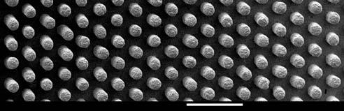

11 Micropillar Structures fabricated by VPP

12 Alternative Fabrication Technique Gel casting CERAMIC POWDER ORGANIC MONOMER SOLVENT DISPERSENT Capability of producing complex parts Homogeneous material properties MIXING SLURRY Rapid forming circle INITIATOR Deairing Low capital equipment cost. CASTING Drying DE-MOULDING PZT slurry Microsized mould De-moulding SINTERING Flow chart of gel casting process. Gl Gel casting for piezocomposite it fabrication.


13 Micropillar Structures fabricated by Gel casting


14 Other pillar shapes and configurations Gel casting

 d 33")


15 Gel casting Vs VPP Comparison of microstructure and properties of sintered bulk ceramics (TRS610C) Gel cast VPP Sample Density (g/cm 3 ) d 33 (pc/n) k t Permitivity Dielectric loss Gel casting 770± 7.70 ± ± ± 0.56 ± VPP 7.65 ± ± ±
16 Piezocomposite Material Characterisation Material parameters determined by fitting electrical impedance to model Representative results for high frequency composite: Resonant frequency: 30 MHz Ceramic volume fraction: 50 % k T = d 33 = 130 pm/v Z A = 17 MRayl ε S RS = 460 Parameters indicative of significant potential for biomedical imaging D. MacLennan, et al., "Fundamental performance characterisation of high frequency piezocomposites made with net-shape viscous polymer processing for medical ultrasound transducers," in Proceedings 2008 IEEE Ultrasonics Symposium, pp , 2008.
17 Single Element Transducers

 Image of mouse subcutaneous tumour xenograft acquired by")
18 30MHz single element transducers Transducer: piezoelectric composite, 1.6 mm diameter, 3 mm geometric focus Piezoelectric composite: 20 μm diameter pillars 29 μm pitch, hexagonal packing lapped to 54 μm thick Packaged and backed with tungsten-loaded epoxy Depth (mm) mm Lateral Position (mm) Image of mouse subcutaneous tumour xenograft acquired by mechanically scanning transducer across specimen
19 Process Improvements for transducer arrays

20 Advanced surface finishing Surfaces of composite must be flat, parallel and smooth in preparation for photolithography After standard processing, the two dissimilar materials in the composite retain surface relief Lapping and polishing processes have been adapted to provide flat and smooth surfaces Epoxy Ceramic Standard processing: ~1 µm height difference Advanced processing: 60 nm height difference
21 Electrode Patterning Lift-off photolithography p process adapted for patterning electrodes on composite material Solvent-resistant epoxy used for composite fill Excellent edge definition and adhesion have been obtained Composite Substrate Deposit Photoresists Expose Develop Expose Develop Deposit Remove Electrodes Photoresists


22 Mask-based Interconnect Standard wirebonding of array element electrodes to flex-circuits does not scale well for arrays above 50 MHz. Silicon wafer interconnect t solution enables wafer scale production and can be used as a platform for further electronics integration. Array substrate Silicon wafer with electroplated and patterned electrodes and bond pads Array substrate connected to contact pads on silicon wafer with flip-chip bonding process
23 Transducer Arrays


24 30MHz linear arrays Arrays: 20 and 32 element designs, 30 μm wide, 50 μm pitch Piezoelectric composite: 20 μm diameter pillars, 29 μm pitch, hexagonal packing, lapped to 55 μm thick Wired, packaged and backed with unloaded epoxy for preliminary testing Fan-out and bond pads for preliminary testing 2 mm x 2 mm composite Array substrate with patterned electrodes defining elements Array electrodes Ceramic Pillars

 4 5 Synthetic aperture")

25 30MHz linear arrays Time: 20 ns/div Pulse: 20 mv/div Frequency: 20 MHz/div Spectrum: 20 db/div Pulse Spectrum Pulse-echo response of single element from quartz flat Centre Frequency: 31 MHz, Bandwidth: 50 % Packaged Prototype Array Dep pth (mm) 4 5 Synthetic aperture Image of 1 mm cylindrical cyst phantom in scattering background. y p, p µ Synthesised aperture: 4 mm, pitch: 10 µm Lateral Position (mm)

 Wired, packaged and backed")

26 100MHz linear array pattern Proof of Concept Array: 20 elements, μm wide, 15 μm pitch Piezoelectric composite: 40 μm thick (for 50MHz operation) Wired, packaged and backed with unloaded epoxy for preliminary testing 2mm p 2 mm x 2 mm Composite Composite substrate with patterned array electrodes Electrodes Ceramic Pillars

27 100MHz linear array pattern Array wired to connectors and packaged for testing Array substrate Voltage response Pulse-echo response of single element from quartz flat. Centre Frequency: 51 MHz, Bandwidth: 25 %
28 Electrical Impedance ) Mag gnitude (Ohms) Electrical Impedance of representative element in 30 MHz array Magnitude Phase Frequency (MHz) Phase (deg.) 30 MHz array Thickness mode frequency at 30 MHz Lateral mode at 40 MHz due to unoptimised composite Elements across array have uniform performance Response consistent with expected performance 100 MHz array Elements show piezoelectric response 45 MHz thickness mode Response is highly damped because array pattern very small relative to composite
29 Potential Applications Applications for MHz arrays can be found in the many clinical disciplines which require: - High spatial resolution - Real-time imaging Example: Dermatology High frequency arrays can be used to enhance 3D and reflex transmission imaging (RTI) by varying the focus through the depth of the tissue in real time RTI measures the attenuation of tissue at the focus of a strongly focused transducer RTI with high frequency arrays has potential for improving the accuracy and efficiency of diagnosis of melanoma Example: Ultrasonic and optoacoustic scanning of vasculature The synthetic focusing possible with arrays is required for optoacoustic imaging of oxygenated and deoxygenated blood With high frequency arrays, accurate imaging of microvasculature becomes possible, leading to improved diagnosis and monitoring of many diseases
30 Summary Micromoulding and microfabrication processes have been developed for fabricating fine-scale, HFUS transducer arrays. Micromoulded piezoelectric composites with material properties suitable for high h frequency imaging i have been made. Surface finishing and photolithography o og techniques have been developed and adapted to pattern fine-scale arrays directly on composite surfaces. Prototype arrays have been fabricated and perform as Prototype arrays have been fabricated and perform as expected.
31 Commercial Prospects HFUS is already here! VisualSonics, SonoSite Interest t in HF from most major Ultrasound players Specific applications for HF single element devices Cost effective fabrication for HF Arrays (>15 MHz) required Wide range of potential applications
32 Future Work Optimise piezoelectric composite and array designs for improved performance at 50 MHz and above. Further develop technologies for interconnect between arrays and silicon wafers. Integration of HFUS arrays with electronics to minimise cable issues preliminary demonstration of combining a HFUS transducer with an ASIC in collaboration with Penn State (Bernassau et al, IEEE Ultrasonics Symp, Rome 2009). Application specific programmes.
Heriot-Watt University
 Heriot-Watt University Heriot-Watt University Research Gateway Microfabrication of electrode patterns for high-frequency ultrasound transducer arrays Bernassau, Anne; Garcia-Gancedo, Luis; Hutson, David;
Heriot-Watt University
 Heriot-Watt University Heriot-Watt University Research Gateway Optimization and characterisation of bonding of piezoelectric transducers using anisotropic conductive adhesive Cummins, Gerard; Gao, Jun;
Piezoelectric Polycrystalline (PZT) Components and Wafers
 Components and Wafers") Piezoelectric Polycrystalline (PZT) Components and Wafers Industry Leading Piezoelectric Polycrystalline (PZT) Component Manufacturing and Engineering CTS offers high-performance piezoelectric materials
Piezoelectric Polycrystalline (PZT) Components and Wafers Industry Leading Piezoelectric Polycrystalline (PZT) Component Manufacturing and Engineering CTS offers high-performance piezoelectric materials
Microelectronics. Integrated circuits. Introduction to the IC technology M.Rencz 11 September, Expected decrease in line width
 Microelectronics Introduction to the IC technology M.Rencz 11 September, 2002 9/16/02 1/37 Integrated circuits Development is controlled by the roadmaps. Self-fulfilling predictions for the tendencies
Challenges for Embedded Device Technologies for Package Level Integration
 Challenges for Embedded Device Technologies for Package Level Integration Kevin Cannon, Steve Riches Tribus-D Ltd Guangbin Dou, Andrew Holmes Imperial College London Embedded Die Technology IMAPS-UK/NMI
PRECISION MACHINING & FINISHING. Micron+ NE X T GENERATION MICRON+
 PRECISION MACHINING & FINISHING NE X T GENERATION MICRON+ Toolmakers can achieve highly consistent engineered abrasive tools using, which increases productivity and dramatically improves workpiece quality.
PREPARED FOR: U.S. Army Medical Research and Materiel Command Fort Detrick, Maryland
 AD Award Number: W81XWH-07-1-0231 TITLE: Spectroscopic Photoacoustic Tomography of Prostate Cancer PRINCIPAL INVESTIGATOR: Xueding Wang CONTRACTING ORGANIZATION: University Of Michigan Ann Arbor, MI 48109-1274
Aluminum Nitride Thin Films for High Frequency Smart Ultrasonic Sensor Systems
 18th World Conference on Nondestructive Testing, 16-20 April 2012, Durban, South Africa Aluminum Nitride Thin Films for High Frequency Smart Ultrasonic Sensor Systems Thomas HERZOG, Susan WALTER, Susanne
UV15: For Fabrication of Polymer Optical Waveguides
 CASE STUDY UV15: For Fabrication of Polymer Optical Waveguides Master Bond Inc. 154 Hobart Street, Hackensack, NJ 07601 USA Phone +1.201.343.8983 Fax +1.201.343.2132 main@masterbond.com CASE STUDY UV15:
PREPARED FOR: U.S. Army Medical Research and Materiel Command Fort Detrick, Maryland
 AD Award Number: W81XWH-07-1-0231 TITLE: Spectroscopic Photoacoustic Tomography of Prostate Cancer PRINCIPAL INVESTIGATOR: Xueding Wang CONTRACTING ORGANIZATION: University Of Michigan Ann Arbor, MI 48109-1274
PIEZOELECTRIC PLATES. Features:
 PIEZOELECTRIC PLATES Morgan Advanced Materials is a world leader in the design and manufacture of complex electronic ceramic components and assemblies used in a wide range of applications and cutting edge
Surface Micromachining of Uncooled Infrared Imaging Array Using Anisotropic Conductive Film
 Surface Micromachining of Uncooled Infrared Imaging Array Using Anisotropic Conductive Film Weiguo Liu, Lingling Sun, Weiguang Zhu, Ooi Kiang Tan Microelectronics Center, School of Electrical and Electronic
CX Thin Fil s. Resistors Attenuators Thin-Film Products Thin-Film Services. ISO 9001:2008 RoHS/REACH Compliant ITAR Compliant
 CX Thin Fil s Resistors Attenuators Thin-Film Products Thin-Film Services www.cxthinfilms.com ISO 9001:2008 RoHS/REACH Compliant ITAR Compliant www.cxthinfilms.com sales@cxthinfilms.com +1 (401) 461-5500
Session: P3J TRANSDUCER MATERIALS III Chair: Y. Takeuchi Kagoshima University P3J-1
 edges of the fluid boundary. First, we investigated the effect of the reservoirs on the membrane resonances. Our results showed that in the presence of a reservoir the resonance frequency decreased, the
Electrical and Fluidic Microbumps and Interconnects for 3D-IC and Silicon Interposer
 Electrical and Fluidic Microbumps and Interconnects for 3D-IC and Silicon Interposer Li Zheng, Student Member, IEEE, and Muhannad S. Bakir, Senior Member, IEEE Georgia Institute of Technology Atlanta,
Supporting Information: Model Based Design of a Microfluidic. Mixer Driven by Induced Charge Electroosmosis
 Supporting Information: Model Based Design of a Microfluidic Mixer Driven by Induced Charge Electroosmosis Cindy K. Harnett, Yehya M. Senousy, Katherine A. Dunphy-Guzman #, Jeremy Templeton * and Michael
Application of Electronic Devices for Aerosol Deposition Methods
 Application of Electronic Devices for Aerosol Deposition Methods NAKADA Masafumi, KAWAKAMI Toshihiro, IWANAMI Mizuki, OHASHI Keishi Abstract Oxide materials have superior functional characteristics that
Preface Preface to First Edition
 Contents Foreword Preface Preface to First Edition xiii xv xix CHAPTER 1 MEMS: A Technology from Lilliput 1 The Promise of Technology 1 What Are MEMS or MST? 2 What Is Micromachining? 3 Applications and
Meggitt Sensing Systems. This document and the information in it is proprietary and is the property of Meggitt Sensing Systems. It may not be copied
 Meggitt Sensing Systems. This document and the information in it is proprietary and is the property of Meggitt Sensing Systems. It may not be copied or disclosed to a third party or used for any purpose
Energy-Efficient Strain Gauges for the Wireless Condition Monitoring Systems in Mechanical Engineering
 6th European Workshop on Structural Health Monitoring - We.4.C.2 More info about this article: http://www.ndt.net/?id=14052 Energy-Efficient Strain Gauges for the Wireless Condition Monitoring Systems
Meso A/SMP Approach. Abstract
 Abstract Additive/Subtractive Material Processing for Mesoscopic Parts Yih-Lin Cheng, Jurgen Stampfl, Rudolf Leitgeb, and Fritz B. Prinz Stanford University, Stanford, CA Mesoscopic additive/subtractive
BUILD TO PERFORMANCE RF Customized Ceramic Thin Film Filters
 Vectron Thin Film Filters BUILD TO PERFORMANCE RF Customized Ceramic Thin Film Filters Anton Buchleitner, Vectron International VECTRON Thin Film Filters bandwidth / MHz Features: 1 1 1 1 1 1.1.1.1.1.1.1
KGC SCIENTIFIC Making of a Chip
 KGC SCIENTIFIC www.kgcscientific.com Making of a Chip FROM THE SAND TO THE PACKAGE, A DIAGRAM TO UNDERSTAND HOW CPU IS MADE? Sand CPU CHAIN ANALYSIS OF SEMICONDUCTOR Material for manufacturing process
NRC Publications Archive Archives des publications du CNRC
 NRC Publications Archive Archives des publications du CNRC Flexible ultrasonic transducers for structural health monitoring of pipes at high temperature Shih, J. -L.; Kobayashi, Makiko; Jen, Cheng-Kue
A Study of Microwave Behavior of a Thin-Print Gold Ink
 A Study of Microwave Behavior of a Thin-Print Gold Ink By David J. Nabatian KOARTAN Microelectronic Interconnect Materials Mountain Ridge Business Park, Unit B2, 248 Sussex Tpk., Randolph, NJ 07869 Phone:
Lead-Free Solder Bump Technologies for Flip-Chip Packaging Applications
 Lead-Free Solder Bump Technologies for Flip-Chip Packaging Applications Zaheed S. Karim 1 and Jim Martin 2 1 Advanced Interconnect Technology Ltd. 1901 Sunley Centre, 9 Wing Yin Street, Tsuen Wan, Hong
Advancements in the Design and Fabrication of Ultrasound Transducers for Extreme Temperatures
 Advancements in the Design and Fabrication of Ultrasound Transducers for Extreme Temperatures by Christopher Bosyj A thesis submitted in conformity with the requirements for the degree of Master of Applied
Packaging Commercial CMOS Chips for Lab on a Chip Integration
 Supporting Information for Packaging Commercial CMOS Chips for Lab on a Chip Integration by Timir Datta-Chaudhuri, Pamela Abshire, and Elisabeth Smela Biocompatibility Although the supplier s instructions
We get small. Micron-scale Circuits and Structures from Prototype through Production
 We get small. Micron-scale Circuits and Structures from Prototype through Production Smaller, tighter, better. When you need to produce ultra-small electrical, mechanical and optical components to extreme
SLIM TM, High Density Wafer Level Fan-out Package Development with Submicron RDL
 2017 IEEE 67th Electronic Components and Technology Conference SLIM TM, High Density Wafer Level Fan-out Package Development with Submicron RDL YoungRae Kim 1, JaeHun Bae 1, MinHwa Chang 1, AhRa Jo 1,
Beam Leads. Spider bonding, a precursor of TAB with all-metal tape
 Beam Leads The vast majority of chips are intended for connection with thermosonic bonds: all other methods require some modification to the wafer. As early as 1972, Jordan described three gang-bonding
SINGLE CRYSTAL SAPPHIRE
 SINGLE CRYSTAL SAPPHIRE Single Crystal Sapphire plays an everincreasingly important role as a material for high reliability Opto-Electronics today due to excellent mechanical characteristics, chemical
PROCESS FLOW AN INSIGHT INTO CMOS FABRICATION PROCESS
 Contents: VI Sem ECE 06EC63: Analog and Mixed Mode VLSI Design PROCESS FLOW AN INSIGHT INTO CMOS FABRICATION PROCESS 1. Introduction 2. CMOS Fabrication 3. Simplified View of Fabrication Process 3.1 Alternative
Micro-fluidic Chip for Flow Cytometry Jeff Wang
 Micro-fluidic Chip for Flow Cytometry Jeff Wang September, 2015 ABSTRACT This lab course is intended to give students hands-on experience with microfabrication. The project is to make a micro-fluidic chip
Preparation of PZT(53/47) thick films deposited by a dip-coating process
 thick films deposited by a dip-coating process") Microelectronic Engineering 66 (003) 865 871 www.elsevier.com/ locate/ mee Preparation of PZT(53/47) thick s deposited by a dip-coating process * Xi-Yun He, Ai-Li Ding, Xin-Sen Zheng, Ping-Sun Qiu, Wei-Gen
Microelectronic Engineering 66 (003) 865 871 www.elsevier.com/ locate/ mee Preparation of PZT(53/47) thick s deposited by a dip-coating process * Xi-Yun He, Ai-Li Ding, Xin-Sen Zheng, Ping-Sun Qiu, Wei-Gen
ADHESIVE CURE MONITORING WITH ACOUSTIC METHOD
 ADHESIVE CURE MONITORING WITH ACOUSTIC METHOD I. Severina, E. Maeva Industrial Research Chair In Applied Solid State Physics and Material Characterization, University of Windsor, Windsor, Canada Abstract:
A Modeling Platform for Ultrasonic Immersion Testing of Polycrystalline Materials with Flaws
 11th European Conference on Non-Destructive Testing (ECNDT 2014), October 6-10, 2014, Prague, Czech Republic A Modeling Platform for Ultrasonic Immersion Testing of Polycrystalline Materials with Flaws
Research Article A Surface Acoustic Wave Ethanol Sensor with Zinc Oxide Nanorods
 Smart Materials Research Volume 2012, Article ID 210748, 4 pages doi:10.1155/2012/210748 Research Article A Surface Acoustic Wave Ethanol Sensor with Zinc Oxide Nanorods TimothyJ.Giffney,Y.H.Ng,andK.C.Aw
Piezoelectric Thick Film Technology Integrated Self-sustained Systems for Industrial
 InSensor Piezoelectric Thick Film Technology Integrated Self-sustained Systems for Industrial Applications Wanda W. Wolny, Rasmus Lou-Moeller, Erling Ringgaard, Konstantin Astafjev and Tomasz Zawada Meggitt
QUANTITATIVE NONDESTRUCTIVE EVALUATION OF ADHESIVE BOND STRENGTH
 QUANTITATIVE NONDESTRUCTIVE EVALUATION OF ADHESIVE BOND STRENGTH INTRODUCTION Jonathan H. Gosse Materials and Processes Boeing Aerospace Company Leroy R. Hause Quality Assurance Boeing Aerospace Company
Advanced Polymers And Resists For Nanoimprint Lithography
 Q U A L I T Y A S S U R A N C E MICROSYSTEMS & NANOSYSTEMS SPECIAL REPORT Advanced Polymers And Resists For Nanoimprint Lithography Numerous polymer systems specifically designed for nanoimprint lithography
Embedding of Active Components in LCP for Implantable Medical Devices
 44 th IMAPS New England Symposium 2017 Embedding of Active Components in LCP for Implantable Medical Devices Dr. Eckardt Bihler and Dr. Marc Hauer, Dyconex AG Susan Bagen, PE, Micro Systems Technologies,
This Appendix discusses the main IC fabrication processes.
 IC Fabrication B B.1 Introduction This Appendix discusses the main IC fabrication processes. B.2 NMOS fabrication NMOS transistors are formed in a p-type substrate. The NMOS fabrication process requires
Use of Piezoelectric Films for NDT Applications
 ECNDT 2006 - We.2.1.3 Use of Piezoelectric Films for NDT Applications Silvère BARUT, EADS Corporate Research Center, Colomiers, France Abstract. Poly(vinylidene fluoride) i.e. (PVDF) films and its copolymer
An ultrasonic volumetric scanner for image-guided surgery
 International Congress Series 1230 (2001) 190 196 An ultrasonic volumetric scanner for image-guided surgery Jeremy Johnson a,b, *,Ömer Oralkan b, Kambiz Kaviani b, Utkan Demirci b, Mustafa Karaman b, Pierre
Nano- And Micro-Filled Conducting Adhesives For Z-axis Interconnects
 Nano- And Micro-Filled Conducting Adhesives For Z-axis Interconnects We take a look at micro-filled epoxy-based conducting adhesives modified with nanoparticles for z- axis interconnections, especially
Cost Effective 3D Glass Microfabrication for Advanced Packaging Applications
 Cost Effective 3D Glass Microfabrication for Advanced Packaging Applications Authors: Jeb. H Flemming, Kevin Dunn, James Gouker, Carrie Schmidt, Roger Cook ABSTRACT Historically, while glasses have many
Atul Gupta, Eric Snyder, Christiane Gottschalk, Kevin Wenzel, James Gunn
 First Demonstration of Photoresist Cleaning for Fine-Line RDL Yield Enhancement by an Innovative Ozone Treatment Process for Panel Fan-out and Interposers Atul Gupta, Eric Snyder, Christiane Gottschalk,
Challenges of Fan-Out WLP and Solution Alternatives John Almiranez
 Challenges of Fan-Out WLP and Solution Alternatives John Almiranez Advanced Packaging Business Development Asia Introduction to Fan-Out WLP Introduction World of mobile gadgetry continues to rapidly evolve
Welding characteristics and structures of same and different metal specimens using ultrasonic complex vibration welding equipments
 Proceedings of 20 th International Congress on Acoustics, ICA 2010 23-27 August 2010, Sydney, Australia Welding characteristics and structures of same and different metal specimens using ultrasonic complex
Low Voltage Single Crystal Actuators
 Low Voltage Single Crystal Actuators Xiaoning Jiang *a, Paul W. Rehrig a, Jun Luo a, Wesley S. Hackenberger a Shujun Zhang b, and Thomas R. Shrout b a TRS Technologies, Inc. 282 East College Avenue, Suite
Miniature fibre optic probe for minimally invasive photoacoustic sensing
 Miniature fibre optic probe for minimally invasive photoacoustic sensing Sunish J. Mathews*, Edward Z. Zhang, Adrien E. Desjardins and Paul C. Beard Department of Medical Physics and Biomedical Engineering,
Qualification and Performance Specification for High Frequency (Microwave) Printed Boards
 Printed Boards") Qualification and Performance Specification for High Frequency (Microwave) Printed Boards Developed by the High Speed/High Frequency Board Performance Subcommittee (D-22) of the High Speed/High Frequency
Qualification and Performance Specification for High Frequency (Microwave) Printed Boards Developed by the High Speed/High Frequency Board Performance Subcommittee (D-22) of the High Speed/High Frequency
Important note To cite this publication, please use the final published version (if applicable). Please check the document version above.
. Please check the document version above.") Delft University of Technology Intravascular Ultrasound at the Tip of a Guidewire Concept and First Assembly Steps Stoute, Ronald; Louwerse, Marcus; Henneken, VA; Dekker, Ronald DOI 10.1016/j.proeng.2016.11.461
Delft University of Technology Intravascular Ultrasound at the Tip of a Guidewire Concept and First Assembly Steps Stoute, Ronald; Louwerse, Marcus; Henneken, VA; Dekker, Ronald DOI 10.1016/j.proeng.2016.11.461
R&D STATUS REPORT. CONTRACTOR: Materials Systems Inc. CONTRACT AMOUNT: $1,077,052 CONTRACT NO.: N C-0323 AMOUNT FUNDED: $593,606
 MSI Materials Systems Inc. R&D STATUS REPORT CONTRACTOR: Materials Systems Inc. CONTRACT AMOUNT: $1,077,052 CONTRACT NO.: N00014-97-C-0323 AMOUNT FUNDED: $593,606 EFFECTIVE DATE OF CONTRACT: 5 August 1997
Heriot-Watt University
 Heriot-Watt University Heriot-Watt University Research Gateway A highly compact packaging concept for ultrasound transducer arrays embedded in neurosurgical needles Schiavone, Giuseppe; Jones, Tom; Price,
ACMC/SAMPE Conference on Marine Composites Plymouth, September 2003 (ISBN )
") PERFORMANCE OF AUTOMATED ULTRASONIC INSPECTION OF LARGE-SCALE SANDWICH STRUCTURES IN NAVAL SHIPS ABSTRACT Thomas Wulf Plastics and Composites, FORCE Technology, DK-9220 Aalborg East, Denmark On basis of
PERFORMANCE OF AUTOMATED ULTRASONIC INSPECTION OF LARGE-SCALE SANDWICH STRUCTURES IN NAVAL SHIPS ABSTRACT Thomas Wulf Plastics and Composites, FORCE Technology, DK-9220 Aalborg East, Denmark On basis of
HYPRES. Hypres MCM Process Design Rules 04/12/2016
 HYPRES Hypres MCM Process Design Rules 04/12/2016 Direct all inquiries, questions, comments and suggestions concerning these design rules and/or HYPRES fabrication to: Daniel T. Yohannes Tel. (914) 592-1190
New Technology for High-Density LSI Mounting in Consumer Products
 New Technology for High-Density Mounting in Consumer Products V Hidehiko Kira V Akira Takashima V Yukio Ozaki (Manuscript received May 29, 2006) The ongoing trend toward downsizing and the growing sophistication
Printed Thermoelectric, Piezoelectric and Pyroelectric Energy Harvesters
 Printed Thermoelectric, Piezoelectric and Pyroelectric Energy Harvesters Professor Robert Dorey, Chair of Nanomaterials Thursday, 09 April 2015 1 Introduction Harvesting using films Creating film harvesters
A Multilayer Process for 3D-Molded-Interconnect-Devices to Enable the Assembly of Area-Array Based Package Types
 A Multilayer Process for 3D-Molded-Interconnect-Devices to Enable the Assembly of Area-Array Based Package Types T. Leneke and S. Hirsch TEPROSA Otto-von-Guericke University Magdeburg, Germany thomas.leneke@teprosa.de
LTCC SYSTEMS and LTCC DESIGN RULES
 LTCC SYSTEMS and LTCC DESIGN RULES Low Temperature Co-fired Ceramic revision status: G page 1 of 19 Table of Contents: 1 General page 3 2 Commercial LTCC tape systems page 4 3 Design possibilities page
Silicon Wafer Processing PAKAGING AND TEST
 Silicon Wafer Processing PAKAGING AND TEST Parametrical test using test structures regularly distributed in the wafer Wafer die test marking defective dies dies separation die fixing (not marked as defective)
Polymer Microfabrication: Methods and Application
 Polymer Microfabrication: Methods and Application Institute for Applied Materials & Department of Microsystems Engineering (IMTEK) at University of Freiburg KIT University of the State of Baden-Wuerttemberg
General Introduction to Microstructure Technology p. 1 What is Microstructure Technology? p. 1 From Microstructure Technology to Microsystems
 General Introduction to Microstructure Technology p. 1 What is Microstructure Technology? p. 1 From Microstructure Technology to Microsystems Technology p. 9 The Parallels to Microelectronics p. 15 The
Scanning Electron Microscope & Surface Analysis. Wageningen EM Centre Marcel Giesbers
 Scanning Electron Microscope & Surface Analysis Wageningen EM Centre Marcel Giesbers Scanning Electron Microscope & Surface Analysis SEM vs Light Microscope and Transmission EM Secondary Electron Imaging
Material based challenge and study of 2.1, 2.5 and 3D integration
 1 Material based challenge and study of 2.1, 2.5 and 3D integration Toshihisa Nonaka Packaging Solution Center R&D Headquarters Hitachi Chemical Co., Ltd., Sep. 8, 2016 Hitachi Chemical Co., Ltd. 2010.
NanoSystemsEngineering: NanoNose Final Status, March 2011
 1 NanoSystemsEngineering: NanoNose Final Status, March 2011 The Nanonose project is based on four research projects (VCSELs, 3D nanolithography, coatings and system integration). Below, the major achievements
Monitoring Of Adhesive Cure Process and Following Evaluation of Adhesive Joint Structure by Acoustic Techniques
 ECNDT 006 - We... Monitoring Of Adhesive Cure Process and Following Evaluation of Adhesive Joint Structure by Acoustic Techniques Elena Yu. MAEVA, Ina SEVIARYNA, Gilbert B. CHAPMAN, Fedar M. SEVERIN University
Mostafa Soliman, Ph.D. May 5 th 2014
 Mostafa Soliman, Ph.D. May 5 th 2014 Mostafa Soliman, Ph.D. 1 Basic MEMS Processes Front-End Processes Back-End Processes 2 Mostafa Soliman, Ph.D. Wafers Deposition Lithography Etch Chips 1- Si Substrate
m-mold SHAPE DEPOSITION MANUFACTURING OF CERAMIC PARTS
 m-mold SHAPE DEPOSITION MANUFACTURING OF CERAMIC PARTS S.W. NAM, J. STAMPFL, H.C. LIU, S. KANG, F. B. PRINZ Rapid Prototyping Laboratory, Building 530, Room 226, Stanford University, Stanford CA 94305,
Method For Stripping Copper In Damascene Interconnects >>>CLICK HERE<<<
 Method For Stripping Copper In Damascene Interconnects Damascene, or acid copper plating baths, have been in use since the mid 19th century on decorative items and machinery.1,2 The process generally uses
Characterisation of Fe-Ni amorphous thin films for possible magnetostrictive sensor applications
 Characterisation of Fe-Ni amorphous thin films for possible magnetostrictive sensor applications Contents 9.1 Introduction 9.2 Experiment 9.3 Results and Discussions 9.4 Conclusion 9.1 Introduction Magnetostrictive
Polymer Microfabrication (Part II) Prof. Tianhong Cui, Mechanical Engineering ME 8254
 Prof. Tianhong Cui, Mechanical Engineering ME 8254") Polymer Microfabrication (Part II) Prof. Tianhong Cui, Mechanical Engineering ME 8254 Other Polymer Techniques Embossing Low cost High throughput Structures as small as 25 nm Injection molding Features
Polymer Microfabrication (Part II) Prof. Tianhong Cui, Mechanical Engineering ME 8254 Other Polymer Techniques Embossing Low cost High throughput Structures as small as 25 nm Injection molding Features
Oerlikon PVD production solutions for piezoelectric materials
 Oerlikon PVD production solutions for piezoelectric materials Workshop PiezoMEMS Aachen,18. /19.05.2010 M. Kratzer Oerlikon Systems R&D Oerlikon company and products Thin films used for SAW, BAW, MEMS,
Supporting Online Material for
 www.sciencemag.org/cgi/content/full/315/5817/1385/dc1 Supporting Online Material for Super Plastic Bulk Metallic Glasses at Room Temperature Yan Hui Liu, Gang Wang, Ru Ju Wang, De Qian Zhao, Ming Xiang
Technology Drivers for Plasma Prior to Wire Bonding
 Technology Drivers for Plasma Prior to Wire Bonding James D. Getty Nordson MARCH Concord, CA, USA info@nordsonmarch.com Technology Drivers for Plasma Prior to Wire Bonding Page 1 ABSTRACT Advanced packaging
VLSI Design and Simulation
 VLSI Design and Simulation CMOS Processing Technology Topics CMOS Processing Technology Semiconductor Processing How do we make a transistor? Fabrication Process Wafer Processing Silicon single crystal
EE 330 Lecture 9. IC Fabrication Technology Part 2
 EE 330 Lecture 9 IC Fabrication Technology Part 2 Quiz 8 A 2m silicon crystal is cut into wafers using a wire saw. If the wire diameter is 220um and the wafer thickness is 350um, how many wafers will this
Meggitt Sensing Systems. This document and the information in it is proprietary and is the property of Meggitt Sensing Systems. It may not be copied
 Meggitt Sensing Systems. This document and the information in it is proprietary and is the property of Meggitt Sensing Systems. It may not be copied or disclosed to a third party or used for any purpose
Chapter 3 Silicon Device Fabrication Technology
 Chapter 3 Silicon Device Fabrication Technology Over 10 15 transistors (or 100,000 for every person in the world) are manufactured every year. VLSI (Very Large Scale Integration) ULSI (Ultra Large Scale
Gold to gold thermosonic bonding Characterization of bonding parameters
 Gold to gold thermosonic bonding Characterization of bonding parameters Thi Thuy Luu *1, Hoang-Vu Nguyen 1, Andreas Larsson 2, Nils Hoivik 1 and Knut E.Aasmundtveit 1 1: Institute of Micro and Nanosystems
Piezoelectric ceramics test for crack detection
 White paper: Technical-scientific informative ITC-01 / ATCP Piezoelectric ceramics test for crack detection ATCP Physical Engineering www.atcp-ndt.com Authors: A. Henrique Alves P. (Pereira, A.H.A.) Cesar
Alumina/Epoxy Nanocomposite Matching Layers for High-Frequency Ultrasound Transducer Application
 IEEE Transactions on Ultrasonics, Ferroelectrics, and Frequency Control, vol. 56, no. 1, January 2009 213 Alumina/Epoxy Nanocomposite Matching Layers for High-Frequency Ultrasound Transducer Application
Battery Bonding NOT JUST MACHINES. BUT BONDING SOLUTIONS.
 PRODUCT-BROCHURE Battery Bonding For the production of battery packs, F & K DELVOTEC always offers the perfect solution for the highest quality products with our ultrasonic bonding and ultrasonic laserbonding
Change in stoichiometry
 Measurement of Gas Sensor Performance Gas sensing materials: 1. Sputtered ZnO film (150 nm (Massachusetts Institute of Technology) 2. Sputtered SnO 2 film (60 nm) (Fraunhofer Institute of Physical Measurement
Low-temperature, Simple and Fast Integration Technique of Microfluidic Chips by using a UV-curable Adhesive
 Low-temperature, Simple and Fast Integration Technique of Microfluidic Chips by using a UV-curable Adhesive Supplementary Information Channel fabrication Glass microchannels. A borosilicate glass wafer
Flip Chip - Integrated In A Standard SMT Process
 Flip Chip - Integrated In A Standard SMT Process By Wilhelm Prinz von Hessen, Universal Instruments Corporation, Binghamton, NY This paper reviews the implementation of a flip chip product in a typical
OPTIMISED CURING OF SILVER INK JET BASED PRINTED TRACES
 Nice, Côte d Azur, France, 27-29 September 2006 OPTIMISED CURING OF SILVER INK JET BASED PRINTED TRACES Z. Radivojevic 1, K. Andersson 1, K. Hashizume 2, M. Heino 1, M. Mantysalo 3, P. Mansikkamaki 3,
Meggitt Sensing Systems. This document and the information in it is proprietary and is the property of Meggitt Sensing Systems. It may not be copied
 Meggitt Sensing Systems. This document and the information in it is proprietary and is the property of Meggitt Sensing Systems. It may not be copied or disclosed to a third party or used for any purpose
A highly compact packaging concept for ultrasound transducer arrays embedded in neurosurgical needles
 DOI 10.1007/s00542-015-2775-1 TECHNICAL PAPER A highly compact packaging concept for ultrasound transducer arrays embedded in neurosurgical needles Giuseppe Schiavone 1 Thomas Jones 1,2 Dennis Price 2
MATERIALS. Silicon Wafers... J 04 J 01. MATERIALS / Inorganics & thin films guide
 J MATERIALS SUBSTRATES Silicon Wafers... J 04 J J 01 MATERIALS SUBSTRATES NEYCO has a complete range of crystal substrates for a wide variety of applications, including Semiconductor, Biotechnology, Nanotechnology,
Fabrication of Smart Card using UV Curable Anisotropic Conductive Adhesive (ACA) Part II: Reliability Performance of the ACA Joints
 Part II: Reliability Performance of the ACA Joints") Fabrication of Smart Card using UV Curable Anisotropic Conductive Adhesive (ACA) Part II: Reliability Performance of the ACA Joints C. W. Tan, Y M Siu, K. K. Lee, *Y. C. Chan & L. M. Cheng Department of
Fabrication of Smart Card using UV Curable Anisotropic Conductive Adhesive (ACA) Part II: Reliability Performance of the ACA Joints C. W. Tan, Y M Siu, K. K. Lee, *Y. C. Chan & L. M. Cheng Department of
Manufacturing Technologies for MEMS and SMART SENSORS
 4 Manufacturing Technologies for MEMS and SMART SENSORS Dr. H. K. Verma Distinguished Professor (EEE) Sharda University, Greater Noida (Formerly: Deputy Director and Professor of Instrumentation Indian
37032 Tours Cedex 1, France e Cranfield University, Bedfordshire MK43 0AL, UK f University of Surrey, Surrey, GU2 7XH, UK
 Fabrication and characterization of annular-array, high-frequency, ultrasonic transducers based on PZT thick film D. Wang a, b, *, E. Filoux c, F. Levassort d, M. Lethiecq d, S.A. Rocks e and R.A. Dorey
COMBINED INVESTIGATION OF EDDY CURRENT AND ULTRASONIC
 COMBINED INVESTIGATION OF EDDY CURRENT AND ULTRASONIC TECHNIQUES FOR COMPOSITE MATERIALS NDE C. W. Davis US Army ATCOM Fort Eustis, VA 23604-5577 S. Nath and J. P. Fulton Analytic Services and Materials,
Improving the piezoelectric properties of thick-film PZT: the influence of paste composition, powder milling process and electrode material
 Sensors and Actuators A 110 (2004) 378 384 Improving the piezoelectric properties of thick-film PZT: the influence of paste composition, powder milling process and electrode material R.N. Torah, S.P. Beeby,
Packaging Technologies for SiC Power Modules
 Packaging Technologies for SiC Power Modules Masafumi Horio Yuji Iizuka Yoshinari Ikeda ABSTRACT Wide bandgap materials such as silicon carbide (SiC) and gallium nitride (GaN) are attracting attention
Influence of nano silver filler content on properties of ink-jet printed structures for microelectronics
 Influence of nano silver filler content on properties of ink-jet printed structures for microelectronics Tomasz Falat 1*, Jan Felba 1, Andrzej Moscicki 2, Anita Smolarek 2, Karlheinz Bock 3 and Detlef
IC Fabrication Technology Part III Devices in Semiconductor Processes
 EE 330 Lecture 10 IC Fabrication Technology Part III Metalization and Interconnects Parasitic Capacitances Back-end Processes Devices in Semiconductor Processes Resistors Diodes Review from Last Lecture