Embedding of Active Components in LCP for Implantable Medical Devices
|
|
|
- Alaina Burke
- 5 years ago
- Views:
Transcription

1 44 th IMAPS New England Symposium 2017 Embedding of Active Components in LCP for Implantable Medical Devices Dr. Eckardt Bihler and Dr. Marc Hauer, Dyconex AG Susan Bagen, PE, Micro Systems Technologies, Inc.
2 BACKGROUND AND GOALS Liquid crystal polymer (LCP) dielectric has been demonstrated as feasible for producing directly implantable, biocompatible structures without the need for hermetic coatings or housings [1,2]. Neural interfaces and electrodes can be fabricated based on flex circuit manufacturing techniques using biocompatible material sets Achieve significantly smaller form factors Incorporate complex features, channels and routings through the use of photolithography and laser drilling Enhancing functionality by embedding active and passive components within the implantable structures thanks to the very low moisture uptake of LCP References: [1] J. Jeung, et al., "A novel multilayered planar coil based on biocompatible liquid crystal polymer for chronic pain implantation," Sensors and Actuators A: Physical, Volume 197, 1 August 2013, pp [2] S.W. Lee, et al., "Development of Microelectrode Arrays for Artificial Retinal Implants Using Liquid Crystal Polymers," IOVS, December 2009, Vol. 50, No. 12, pp

3 LIQUID CRYSTAL POLYMER (LCP) PROPERTIES LCP is a thermoplastic material Operating temperature up to 190 C Melting point at 280 C Can be transfer molded to any shape Density 1.4 g/cm3 Low water absorption < 0.04% Fully biocompatible according to ISO (in vitro cytotoxicity) 3
4 EXAMPLES OF BIOCOMPATIBLE LCP STRUCTURES Electrodes and neural interface structures fabricated on conventional flex circuit manufacturing equipment combined with thin film technology Single layer Biocompatible material Biocompatible conductor Au / Pt pads Multilayer Biocompatible material Biocompatible conductor Biocompatible vias Bioinert package Biocompatible material & conductor Biocompatible vias Embedded dies Gold electrodes exposed on inner layers Gold electrodes on outer layer Gold electrodes on outer layer Gold traces Gold traces Bioinert vias Gold traces Active component or sensor Bioinert vias 4

5 BIOCOMPATIBLE CONDUCTOR TECHNOLOGY Conductor material pure gold Minimum line width 30 µm Minimum spacing between traces 20 µm Conductor thickness between 2 15 µm Line resistance between Ω/cm Resistance has a linear temperature coefficient and can be used to measure temperature Gold traces Gold electrodes Completely Biocompatible Structure LCP lead structure with electrodes on the surface and embedded metal traces from pure gold 5


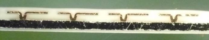
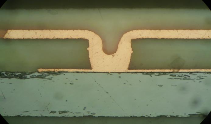
6 NOBLE METAL TRACES AND VIAS Electrode Completely fused LCP embedding the metal traces 75 µm diameter via with 15 µm gold thickness 120 µm wide trace with 15 µm gold thickness LCP 120 µm wide traces with 60 µm spacing in 75 µm thick LCP structure with electrode on top 6

7 SEALED INTERCONNECTS BETWEEN CABLES New fully biocompatible interconnect technology for implanted leads Extension of maximum lead length Solderless & glueless Local applied heat pulse under pressure melts LCP and seals contacts Pull strength 20 N/mm - same as lead body - Technical Roadmap for Packaging in Hearing Aids 7

8 HIRES TIP ELECTRODE High resolution with pure gold traces for biocompatible, neurostimulation electrode Tip width: Distance between electrodes: Electrode diameter: 300 μm 250 μm 100 μm Embedded traces on backside with trace width of 30 μm Metallized via 20 μm 100 μm 8

9 HIGH RESOLUTION ELECTRODE FOR BRAIN INTERFACE Application: Implanted electrode for 4 x 64 Channel EEG for animal tests 16 x 16 Matrix of electrodes with 0.75 mm pitch Pure gold traces with 30 μm line width/spacing Traces embedded in LCP Electrode diameter 75 μm 9
10 METHODS RELIABILITY EVALUATION LCP film used as the dielectric material with noble metal conductors such as Au, Pt and PtIr Appropriate cleaning processes used to ensure biocompatibility of the final structures[3] Mock silicon die patterned with Cu embedded within the LCP to produce test structures for hermeticity studies Long term biostability evaluations performed by soak tests in heated phosphate-buffered saline (PBS) Bend testing at a 0.5 mm radius conducted for mechanical reliability Cross-sectional analysis used to examine regions of failure [3] ISO :2009 Biological evaluation of medical devices Part 1: Evaluation and testing with a risk management process. 10
11 TEST CHIP DESIGN FIGURE 2 Test chip for embedding Manufacturer: TLMI, Austin, Texas Wafer diameter: 150 mm Active wafer diameter: 147 mm Wafer thickness: 100 µm (thinned) Die surface: thermal oxide Adhesion promoter: TiW (sputtered) Metallization: 3 µm copper & gold flash Chip dimensions: 5 x 8 mm Artwork on die Pad size: 250 x 250 µm (thinned) Interdigitized comb structure with 50 µm lines & spaces 11


 4")

12 TEST CHIP EMBEDDED IN LCP 4-layer LCP multilayer build-up 1 Electrode layer (1) 4 2 Redistribution layer (2) Chip pad layer (3) Backside layer (4) 4 12


13 EMBEDDED DIE TEST STRUCTURE FOR SOAK TESTS Contact pads on electrode layer (1) Embedded traces on redistribution layer (2) Embedded die with pads on layer (3) Grid structure on backside (4)


14 TEST CHIP TO OUTLINE DISTANCES Layer 2 copper / outline distance Layer 3 chip artwork / outline distance 14

 LCP with Au traces Pass")
15 BEND TESTING APPARATUS AND METHOD FIGURE 6 TEST LCP STRUCTURE RESULT Bend (radius 0.5 mm) LCP with Au traces Pass 100k cycles 15
16 SOAK TESTING APPARATUS FIGURE 7 16
17 RESULTS Noble metal LCP based neural interface and electrode structures successfully fabricated using conventional flex circuit and thin film processing Structures that undergo specialized cleaning operations pass the ISO cytotoxicity test requirements LCP structures with Au conductors passed PBS soak testing at 77 o C for > 9 months without failure 17
18 PBS SOAK (90 C) TEST RESULTS OF EMBEDDED DIE IN LCP STRUCTURES SAMPLE Time to value below range limit of 10 GΩ [h] 1'536 1' Saturation Value > 1GΩ 1.6 MΩ 14 MΩ 0.9 MΩ 21.5 kω 2 MΩ 3 kω 3 MΩ 5 MΩ 0.2 MΩ A resistance reduction was observed in 9 out of 10 samples, occurring between 168 and C in PBS One sample did not show any reduction of resistance below the range limit of 10 GΩ until hours, when the test was terminated 18
19 Resistance in MΩ SOAK TEST RESULT Trend of resistance of comb structure on embedded die over exposure time in saline solution (PBS at 90 C) Initial resistance level 10 4 GΩ (Measurement range limit 10 GΩ) Defect driven migration along interfaces (within approx. 50h) Plateau of saturation (around MΩ) Soak test time in hours 19
20 FAILURE ANALYSIS Adhesion between laminated layers was found to be reduced significantly after the soaking test, indicating that moisture penetration is likely the reason for reduced resistance in the comb structure Foreign material, which is embedded between the layers, can act as defect side to enhance the moisture migration Further work needed to reduce moisture penetration along the interfaces Evidence of Cu Electromigration Top layer LCP peeled back on failed electrode structures 20
21 RECENT SOAK TEST RESULTS TEST LCP STRUCTURE RESULT Soak test in PBS at 77 C Soak test in PBS at 50 C Soak test in 40% H 2 SO 4 at 50 C Soak test in 80% H 2 SO 4 at 50 C LCP with Au traces LCP with Cu traces, embedded die LCP with Cu traces, embedded die LCP with Cu traces, embedded die > 9 months continuous (equivalent to 15 years implanted in body) Ongoing test (no measureable drop in resistance after >1800 hours) Ongoing test (no measureable drop in resistance after >1800 hours) Ongoing test (no measureable drop in resistance after >1800 hours) 21
22 CONCLUSIONS Biocompatible neural interfaces and electrode structures can be fabricated from LCP dielectric and noble metal conductors on conventional flex circuit and thin film manufacturing equipment. Passive structures have shown initial feasibility for long term biostability based on PBS soak testing. Structures with embedded die show initial promise for biostability, but further process optimization is needed. The results demonstrate that a new material set comprised of LCP with noble metals is feasible for producing complex implantable structures for neuromodulation applications. 22
23 REFERENCES [1] J. Jeung, et al., "A novel multilayered planar coil based on biocompatible liquid crystal polymer for chronic pain implantation," Sensors and Actuators A: Physical, Volume 197, 1 August 2013, pp [2] S.W. Lee, et al., "Development of Microelectrode Arrays for Artificial Retinal Implants Using Liquid Crystal Polymers," IOVS, December 2009, Vol. 50, No. 12, pp [3] ISO :2009 Biological evaluation of medical devices Part 1: Evaluation and testing with a risk management process. 23


24 Thank you for your attention. DYCONEX AG Switzerland 24
Flexible Substrates for Smart Sensor Applications
 Flexible Substrates for Smart Sensor Applications A novel approach that delivers miniaturized, hermetic, biostable and highly reliable smart sensor modules. AUTHORS Dr. Eckardt Bihler, Dr. Marc Hauer,
Liquid Crystal Polymer Substrates to Enable Advanced RF and Medical Applications
 Liquid Crystal Polymer Substrates to Enable Advanced RF and Medical Applications Susan Bagen & Brian Sinclair MST Inc. Eckardt Bihler, Marc Hauer & Daniel Schulze DYCONEX AG New England 42nd Symposium
iniaturization of medical devices thanks to flexible substrates ISO 9001 certified
 iniaturization of medical devices thanks to flexible substrates 04-12-2012 Hightec MC Presentation 2 Medical industry is clearly and urgently in need of the development of advanced interconnection solutions
Manufacturing Capacity
 Capability List Manufacturing Capacity QTA & Prototype Layer : 1L ~32 L Impedance Board Ball Grid Array ( BGA ) Blind/ Buried Via Micro Via ( Laser Drilling) Flex /Rigid Flexible PCB Series Orders Layer
Biostability and corrosion resistance of a biocompatible encapsulation and interconnect technology for implantable electronics
 Biostability and corrosion resistance of a biocompatible encapsulation and interconnect technology for implantable electronics Maaike Op de Beeck Karen Qian, Karl Malachowski, Bishoy Morcos, Alex Radisic,
ALTIUMLIVE 2018: FLEX: SOMETHING NEW FOR EVERYONE
 ALTIUMLIVE 2018: FLEX: SOMETHING NEW FOR EVERYONE Tara Dunn Omni PCB President San Diego October 5, 2018 Applications That Span Technology Today s Discussion: 1. Basic processing steps for both subtractive
We get small. Micron-scale Circuits and Structures from Prototype through Production
 We get small. Micron-scale Circuits and Structures from Prototype through Production Smaller, tighter, better. When you need to produce ultra-small electrical, mechanical and optical components to extreme
Building HDI Structures using Thin Films and Low Temperature Sintering Paste
 Building HDI Structures using Thin Films and Low Temperature Sintering Paste Catherine Shearer, James Haley and Chris Hunrath Ormet Circuits Inc. - Integral Technology California, USA chunrath@integral-hdi.com
Embedded Passives..con0nued
 Embedded Passives..con0nued Why Embedded Passives? Improves the packaging efficiency System-on-Package (SOP); SLIM integration Reducing size Eliminating substrate assembly Minimizing solder joint failure
Electrical and Fluidic Microbumps and Interconnects for 3D-IC and Silicon Interposer
 Electrical and Fluidic Microbumps and Interconnects for 3D-IC and Silicon Interposer Li Zheng, Student Member, IEEE, and Muhannad S. Bakir, Senior Member, IEEE Georgia Institute of Technology Atlanta,
Chapter 4 Fabrication Process of Silicon Carrier and. Gold-Gold Thermocompression Bonding
 Chapter 4 Fabrication Process of Silicon Carrier and Gold-Gold Thermocompression Bonding 4.1 Introduction As mentioned in chapter 2, the MEMs carrier is designed to integrate the micro-machined inductor
CLAD MATERIAL ~ FINE CLAD is a solution for high density, low cost PWB.
 ~ CLAD MATERIAL ~ FINE CLAD is a solution for high density, low cost PWB. Principle of bonding technique Principle of bonding technique Step 1 Material A, B In vacuum Step 2 Surface activated treatment
Two Chips Vertical Direction Embedded Miniaturized Package
 Two Chips Vertical Direction Embedded Miniaturized Package Shunsuke Sato, 1 Koji Munakata, 1 Masakazu Sato, 1 Atsushi Itabashi, 1 and Masatoshi Inaba 1 Continuous efforts have been made to achieve seemingly
Microelectronics. Integrated circuits. Introduction to the IC technology M.Rencz 11 September, Expected decrease in line width
 Microelectronics Introduction to the IC technology M.Rencz 11 September, 2002 9/16/02 1/37 Integrated circuits Development is controlled by the roadmaps. Self-fulfilling predictions for the tendencies
Visit
 Practical Applications for Nano- Electronics by Vimal Gopee E-mail: Vimal.gopee@npl.co.uk 10/10/12 Your Delegate Webinar Control Panel Open and close your panel Full screen view Raise hand for Q&A at the
Flexible Printed Circuits Design Guide
 www.tech-etch.com/flex Flexible Printed Circuits Design Guide Multilayer SMT Assembly Selective Plating of Gold & Tin-Lead Fine Line Microvias Cantilevered & Windowed Leads 1 MATERIALS CONDUCTOR Copper
Anti-Counterfeit, Advanced Microelectronics Packaging Solutions for Miniaturized Medical Devices
 Anti-Counterfeit, Advanced Microelectronics Packaging Solutions for Miniaturized Medical Devices Rabindra N. Das, Frank D. Egitto, and How Lin Endicott Interconnect Technologies, Inc., 1093 Clark Street,
MEPTEC Semiconductor Packaging Technology Symposium
 MEPTEC Semiconductor Packaging Technology Symposium Advanced Packaging s Interconnect Technology Process Shift and Direction October 23, 2014 Jay Hayes- Director of Business Development -Bumping and Flip
CX Thin Fil s. Resistors Attenuators Thin-Film Products Thin-Film Services. ISO 9001:2008 RoHS/REACH Compliant ITAR Compliant
 CX Thin Fil s Resistors Attenuators Thin-Film Products Thin-Film Services www.cxthinfilms.com ISO 9001:2008 RoHS/REACH Compliant ITAR Compliant www.cxthinfilms.com sales@cxthinfilms.com +1 (401) 461-5500
Chips Face-up Panelization Approach For Fan-out Packaging
 Chips Face-up Panelization Approach For Fan-out Packaging Oct. 15, 2015 B. Rogers, D. Sanchez, C. Bishop, C. Sandstrom, C. Scanlan, TOlson T. REV A Background on FOWLP Fan-Out Wafer Level Packaging o Chips
A Multilayer Process for 3D-Molded-Interconnect-Devices to Enable the Assembly of Area-Array Based Package Types
 A Multilayer Process for 3D-Molded-Interconnect-Devices to Enable the Assembly of Area-Array Based Package Types T. Leneke and S. Hirsch TEPROSA Otto-von-Guericke University Magdeburg, Germany thomas.leneke@teprosa.de
 Thermo-Mechanical Analysis of Flexible and Stretchable Systems Mario Gonzalez 1, Bart Vandevelde 1, Wim Christiaens 2, Yung-Yu Hsu 1, François Iker 1, Frederick Bossuyt 1, Jan Vanfleteren 1,2, Olaf van
10 Manor Parkway, Suite C Salem, New Hampshire
 Micro-Precision Technologies (MPT) is an independent manufacturer of hybrid integrated circuits, multichip modules, and high-precision thick film substrates for the military, medical, avionics, optoelectronics,
Packaging Commercial CMOS Chips for Lab on a Chip Integration
 Supporting Information for Packaging Commercial CMOS Chips for Lab on a Chip Integration by Timir Datta-Chaudhuri, Pamela Abshire, and Elisabeth Smela Biocompatibility Although the supplier s instructions
Challenges of Fan-Out WLP and Solution Alternatives John Almiranez
 Challenges of Fan-Out WLP and Solution Alternatives John Almiranez Advanced Packaging Business Development Asia Introduction to Fan-Out WLP Introduction World of mobile gadgetry continues to rapidly evolve
Gold Passivated Mechanically Flexible Interconnects (MFIs) with High Elastic Deformation
 with High Elastic Deformation") Gold Passivated Mechanically Flexible Interconnects (MFIs) with High Elastic Deformation Chaoqi Zhang, Hyung Suk Yang, and Muhannad S. Bakir School of Electrical and Computer Engineering Georgia Institute
Gold Passivated Mechanically Flexible Interconnects (MFIs) with High Elastic Deformation Chaoqi Zhang, Hyung Suk Yang, and Muhannad S. Bakir School of Electrical and Computer Engineering Georgia Institute
Challenges for Embedded Device Technologies for Package Level Integration
 Challenges for Embedded Device Technologies for Package Level Integration Kevin Cannon, Steve Riches Tribus-D Ltd Guangbin Dou, Andrew Holmes Imperial College London Embedded Die Technology IMAPS-UK/NMI
High Barrier Multi-Layer Parylene Coating
 High Barrier Multi-Layer Parylene Coating Technology overview Surface Technolgy 2018 Company Profile Swiss company founded in 1979 Experts in Parylene coating technology Parylene Equipment Export rate
Surface Micromachining of Uncooled Infrared Imaging Array Using Anisotropic Conductive Film
 Surface Micromachining of Uncooled Infrared Imaging Array Using Anisotropic Conductive Film Weiguo Liu, Lingling Sun, Weiguang Zhu, Ooi Kiang Tan Microelectronics Center, School of Electrical and Electronic
Embedding Passive and Active Components: PCB Design and Fabrication Process Variations
 Embedding Passive and Active Components: PCB Design and Fabrication Process Variations Vern Solberg Solberg Technical Consulting Saratoga, California USA Abstract Embedding components within the PC board
SLIM TM, High Density Wafer Level Fan-out Package Development with Submicron RDL
 2017 IEEE 67th Electronic Components and Technology Conference SLIM TM, High Density Wafer Level Fan-out Package Development with Submicron RDL YoungRae Kim 1, JaeHun Bae 1, MinHwa Chang 1, AhRa Jo 1,
Welcome to Streamline Circuits Lunch & Learn. Design for Reliability & Cost Reduction of Advanced Rigid-Flex/Flex PCB Technology
 Welcome to Streamline Circuits Lunch & Learn Design for Reliability & Cost Reduction of Advanced Rigid-Flex/Flex PCB Technology Accurate PCB data is critical to the tooling process. Here are some key items
1 Thin-film applications to microelectronic technology
 1 Thin-film applications to microelectronic technology 1.1 Introduction Layered thin-film structures are used in microelectronic, opto-electronic, flat panel display, and electronic packaging technologies.
Hot Pin Pull Method New Test Procedure for the Adhesion Measurement for 3D-MID
 Hot Pin Pull Method New Test Procedure for the Adhesion Measurement for 3D-MID HARTING Mitronics Christian Goth in cooperation with: FAPS Thomas Kuhn, Gerald Gion, Jörg Franke 11 th International Congress
Product-Info 3D-MID. 1. Introduction. 2. Material and manufacturing process. 1/5
 Product-Info 3D-MID 1. Introduction The term 3D-MID (3D moulded interconnect devices) stands for injectionmoulded, three-dimensional circuit carriers that have been in use for many years in various fields
Smart Implants: Packaging Challenges & Solutions. inemi-2010 Berlin TCl/JFZ
 Smart Implants: Packaging Challenges & Solutions Topics 1. Smart Implants and Packaging Challenges 2. Enabling Miniaturisation Processes 3. Successfully Deployed Examples at Valtronic Group What is a Smart
Chapter 2 Capacitive Sensing Electrodes
 Chapter 2 Capacitive Sensing Electrodes The capacitive sensing electrodes on the top of a CMOS chip serve as an interface between the microelectronic readout system and the biological/chemical analyte.
Ultra Fine Pitch Bumping Using e-ni/au and Sn Lift-Off Processes
 Ultra Fine Pitch Bumping Using e-ni/au and Sn Lift-Off Processes Andrew Strandjord, Thorsten Teutsch, and Jing Li Pac Tech USA Packaging Technologies, Inc. Santa Clara, CA USA 95050 Thomas Oppert, and
Australian Journal of Basic and Applied Sciences. Pb-Free Solder Ball Robustness Comparison under AC and TC Reliability Test
 AENSI Journals Australian Journal of Basic and Applied Sciences ISSN:1991-8178 Journal home page: www.ajbasweb.com Pb-Free Solder Ball Robustness Comparison under AC and TC Reliability Test 1,2 Tan Cai
business 0.2 ± 0.01 mm Ø 1 ± 0.01 mm 4 ± 0.01 mm Products & Services
 0.2 ± 0.01 mm Products & Services Ø 1 ± 0.01 mm 4 ± 0.01 mm business EXPERIENCE THE FUTURE OF IMPLANTABLE TECHNOLOGY CorTec stands for cutting-edge technology for the next generation of active implants.
business Products & Services
 business Products & Services TABLE OF CONTENT WELCOME 4 5 5 COMPETENCES 6 8 10 16 OUR SERVICE 18 CorTec GmbH, November 2017. All rights reserved. 3 EXPERIENCE THE FUTURE OF IMPLANTABLE TECHNOLOGY CorTec
Proceedings Demonstration of Intracortical Chronic Recording and Acute Microstimulation Using Novel Floating Neural Probes
 Proceedings Demonstration of Intracortical Chronic Recording and Acute Microstimulation Using Novel Floating Neural Probes Andreas Schander 1, *, Heiko Stemmann 2, Andreas K. Kreiter 2 and Walter Lang
Plasma Etching Rates & Gases Gas ratios affects etch rate & etch ratios to resist/substrate
 Plasma Etching Rates & Gases Gas ratios affects etch rate & etch ratios to resist/substrate Development of Sidewalls Passivating Films Sidewalls get inert species deposited on them with plasma etch Creates
Energy-Efficient Strain Gauges for the Wireless Condition Monitoring Systems in Mechanical Engineering
 6th European Workshop on Structural Health Monitoring - We.4.C.2 More info about this article: http://www.ndt.net/?id=14052 Energy-Efficient Strain Gauges for the Wireless Condition Monitoring Systems
curamik CERAMIC SUBSTRATES AMB technology Design Rules Version #04 (09/2015)
") curamik CERAMIC SUBSTRATES AMB technology Design Rules Version #04 (09/2015) Content 1. Geometric properties 1.01. Available ceramic types / thicknesses... 03 1.02. thicknesses (standard)... 03 3. Quality
curamik CERAMIC SUBSTRATES AMB technology Design Rules Version #04 (09/2015) Content 1. Geometric properties 1.01. Available ceramic types / thicknesses... 03 1.02. thicknesses (standard)... 03 3. Quality
High Performance Alloys. Characteristics
 Alloy Designation EN DIN CEN/TS 13388 UNS High Performance Alloys Chemical Composition percentage We have developed a wide range of high performance alloys with excellent properties regarding conductivity,
Technology Drivers for Plasma Prior to Wire Bonding
 Technology Drivers for Plasma Prior to Wire Bonding James D. Getty Nordson MARCH Concord, CA, USA info@nordsonmarch.com Technology Drivers for Plasma Prior to Wire Bonding Page 1 ABSTRACT Advanced packaging
High Definition Selective Metallization for Printed Electronics
 High Definition Selective Metallization for Printed Electronics Wolfgang Decker VAST FILMS, Ltd. Outline Introduction of VAST FILMS What is Selective Metalization Range of Applications for Selective Metalization
IPC-2221B APPENDIX A Version 2.0 June 2018
 IPC-2221B APPENDIX A Version 2.0 June 2018 A.1 INTRODUCTION This appendix was developed by the IPC 1-10c Test Coupon and Artwork Generation Task Group and is included in this current document revision
Qualification and Performance Specification for Flexible Printed Boards
 Qualification and Performance Specification for Flexible Printed Boards Developed by the Flexible Circuits Performance Specifications Subcommittee (D-12) of the Flexible Circuits Committee (D-10) of IPC
2W, 2512, 4-Terminal, Low Resistance Chip Resistor (Lead / Halogen Free)
") 2W, 2512, 4-Terminal, Low Resistance Chip Resistor (Lead / Halogen Free) 1. Scope This specification applies to 3.2mm x 6.4mm size 2W, fixed metal foil with ceramic carrier current sensing resistors used
2W, 2512, 4-Terminal, Low Resistance Chip Resistor (Lead / Halogen Free) 1. Scope This specification applies to 3.2mm x 6.4mm size 2W, fixed metal foil with ceramic carrier current sensing resistors used
Copper Interconnect Technology
 Tapan Gupta Copper Interconnect Technology i Springer Contents 1 Introduction 1 1.1 Trends and Challenges 2 1.2 Physical Limits and Search for New Materials 5 1.3 Challenges 6 1.4 Choice of Materials 7
DITF ToolKit 1. Standard Substrate Sizes (selected at the factory for optimum process)
") DITF ToolKit 1 DITF Toolkit Substrates Common Substrate Materials Alumina (99.5% min) єr = 9.9 Tan d = 1.5 x10⁻⁴ Aluminum Nitride (K170) єr = 8.9 Tan d = 2.0 x10⁻³ Beryllia (99.5%) єr = 6.7 Tan d = 3.0
DITF ToolKit 1 DITF Toolkit Substrates Common Substrate Materials Alumina (99.5% min) єr = 9.9 Tan d = 1.5 x10⁻⁴ Aluminum Nitride (K170) єr = 8.9 Tan d = 2.0 x10⁻³ Beryllia (99.5%) єr = 6.7 Tan d = 3.0
DESIGN AND FABRICATION OF POLYNORBORNENE- AND LIQUID CRYSTAL POLYMER-BASED ELECTRODE ARRAYS FOR BIOMEDICAL APPLICATIONS ALLISON ELIZABETH HESS
 DESIGN AND FABRICATION OF POLYNORBORNENE- AND LIQUID CRYSTAL POLYMER-BASED ELECTRODE ARRAYS FOR BIOMEDICAL APPLICATIONS by ALLISON ELIZABETH HESS Submitted in partial fulfillment of the requirements For
Challenges and Future Directions of Laser Fuse Processing in Memory Repair
 Challenges and Future Directions of Laser Fuse Processing in Memory Repair Bo Gu, * T. Coughlin, B. Maxwell, J. Griffiths, J. Lee, J. Cordingley, S. Johnson, E. Karagiannis, J. Ehrmann GSI Lumonics, Inc.
Plasma Etching Rates & Gases Gas ratios affects etch rate & etch ratios to resist/substrate
 Plasma Etching Rates & Gases Gas ratios affects etch rate & etch ratios to resist/substrate Development of Sidewalls Passivating Films Sidewalls get inert species deposited on them Creates passivating
Alternatives to Aluminium Metallization
 Alternatives to Aluminium Metallization Technological pressures on the speed and reliability of integrated circuits has caused a need for changes to be made in the choices of materials used for metallization
JOINT INDUSTRY STANDARD
 JOINT INDUSTRY STANDARD AUGUST 1999 Semiconductor Design Standard for Flip Chip Applications ASSOCIATION CONNECTING ELECTRONICS INDUSTRIES Semiconductor Design Standard for Flip Chip Applications About
Plasma Etching Rates & Gases Gas ratios affects etch rate & etch ratios to resist/substrate
 Plasma Etching Rates & Gases Gas ratios affects etch rate & etch ratios to resist/substrate Development of Sidewalls Passivating Films Sidewalls get inert species deposited on them with plasma etch Creates
Three-Dimensional Molded Interconnect Devices (3D-MID)
") Jörg Frank Three-Dimensional Molded Interconnect Devices (3D-MID) Materials, Manufacturing, Assembly and Applica ons for Injec on Molded Circuit Carriers Sample Pages ISBN 978-1-56990-551-7 HANSER Hanser
Jörg Frank Three-Dimensional Molded Interconnect Devices (3D-MID) Materials, Manufacturing, Assembly and Applica ons for Injec on Molded Circuit Carriers Sample Pages ISBN 978-1-56990-551-7 HANSER Hanser
Analog Devices ADSP KS-160 SHARC Digital Signal Processor
 Construction Analysis Analog Devices ADSP-21062-KS-160 SHARC Digital Signal Processor Report Number: SCA 9712-575 Global Semiconductor Industry the Serving Since 1964 17350 N. Hartford Drive Scottsdale,
IMPLEMENTATION OF A FULLY MOLDED FAN-OUT PACKAGING TECHNOLOGY
 IMPLEMENTATION OF A FULLY MOLDED FAN-OUT PACKAGING TECHNOLOGY B. Rogers, C. Scanlan, and T. Olson Deca Technologies, Inc. Tempe, AZ USA boyd.rogers@decatechnologies.com ABSTRACT Fan-Out Wafer-Level Packaging
R Sensor resistance (Ω) ρ Specific resistivity of bulk Silicon (Ω cm) d Diameter of measuring point (cm)
 ρ Specific resistivity of bulk Silicon (Ω cm) d Diameter of measuring point (cm)") 4 Silicon Temperature Sensors 4.1 Introduction The KTY temperature sensor developed by Infineon Technologies is based on the principle of the Spreading Resistance. The expression Spreading Resistance derives
4 Silicon Temperature Sensors 4.1 Introduction The KTY temperature sensor developed by Infineon Technologies is based on the principle of the Spreading Resistance. The expression Spreading Resistance derives
Plasma Etching Rates & Gases Gas ratios affects etch rate & etch ratios to resist/substrate
 Plasma Etching Rates & Gases Gas ratios affects etch rate & etch ratios to resist/substrate Development of Sidewalls Passivating Films Sidewalls get inert species deposited on them with plasma etch Creates
Global Test solutions Conception and production of probe cards for testing microchips
 Global Test solutions Conception and production of probe cards for testing microchips All Technologies Synergie Cad Probe developed differents solution of test, it is became a leader in the design and
Xilinx XC4036EX FPGA
 Construction Analysis Xilinx XC4036EX FPGA Report Number: SCA 9706-544 Global Semiconductor Industry the Serving Since 1964 15022 N. 75th Street Scottsdale, AZ 85260-2476 Phone: 602-998-9780 Fax: 602-948-1925
IMPACT OF MICROVIA-IN-PAD DESIGN ON VOID FORMATION
 IMPACT OF MICROVIA-IN-PAD DESIGN ON VOID FORMATION Frank Grano, Felix Bruno Huntsville, AL Dana Korf, Eamon O Keeffe San Jose, CA Cheryl Kelley Salem, NH Joint Paper by Sanmina-SCI Corporation EMS, GTS
Chapter 3 Silicon Device Fabrication Technology
 Chapter 3 Silicon Device Fabrication Technology Over 10 15 transistors (or 100,000 for every person in the world) are manufactured every year. VLSI (Very Large Scale Integration) ULSI (Ultra Large Scale
Glass Carrier for Fan Out Panel Level Package
 January 25, 2018 NEWS RELEASE Development of HRDP TM Material for Formation of Ultra-Fine Circuits with Glass Carrier for Fan Out Panel Level Package - Aiming for mass production in collaboration with
VLSI Design and Simulation
 VLSI Design and Simulation CMOS Processing Technology Topics CMOS Processing Technology Semiconductor Processing How do we make a transistor? Fabrication Process Wafer Processing Silicon single crystal
Ajay Kumar Gautam [VLSI TECHNOLOGY] VLSI Technology for 3RD Year ECE/EEE Uttarakhand Technical University
![Ajay Kumar Gautam [VLSI TECHNOLOGY] VLSI Technology for 3RD Year ECE/EEE Uttarakhand Technical University](/thumbs/75/72824557.jpg "Ajay Kumar Gautam [VLSI TECHNOLOGY] VLSI Technology for 3RD Year ECE/EEE Uttarakhand Technical University") 2014 Ajay Kumar Gautam [VLSI TECHNOLOGY] VLSI Technology for 3RD Year ECE/EEE Uttarakhand Technical University Page1 Syllabus UNIT 1 Introduction to VLSI Technology: Classification of ICs, Scale of integration,
2014 Ajay Kumar Gautam [VLSI TECHNOLOGY] VLSI Technology for 3RD Year ECE/EEE Uttarakhand Technical University Page1 Syllabus UNIT 1 Introduction to VLSI Technology: Classification of ICs, Scale of integration,
Novel Technique for Flip Chip Packaging of High power Si, SiC and GaN Devices. Nahum Rapoport, Remtec, Inc.
 Novel Technique for Flip Chip Packaging of High power Si, SiC and GaN Devices Nahum Rapoport, Remtec, Inc. 1 Background Electronic Products Designers: under pressure to decrease cost and size Semiconductor
Characterization of Parylene-C Thin Films as an Encapsulation for Neural Interfaces
 Characterization of Parylene-C Thin Films as an Encapsulation for Neural Interfaces Hsu, Jui-Mei 1 ; Kammer, Sascha 2 ; Jung, Erik 3 ; Rieth, Loren 4 ; Normann, Richard 5 ; Solzbacher, Florian 1,4,5 1
Design for Flip-Chip and Chip-Size Package Technology
 Design for Flip-Chip and Chip-Size Package Technology Vern Solberg Solberg Technology Consulting Madison, Wisconsin Abstract As new generations of electronic products emerge they often surpass the capability
NEC 79VR5000 RISC Microprocessor
 Construction Analysis NEC 79VR5000 RISC Microprocessor Report Number: SCA 9711-567 Global Semiconductor Industry the Serving Since 1964 17350 N. Hartford Drive Scottsdale, AZ 85255 Phone: 602-515-9780
Gold to gold thermosonic bonding Characterization of bonding parameters
 Gold to gold thermosonic bonding Characterization of bonding parameters Thi Thuy Luu *1, Hoang-Vu Nguyen 1, Andreas Larsson 2, Nils Hoivik 1 and Knut E.Aasmundtveit 1 1: Institute of Micro and Nanosystems
Chapter 11: Passives: Discrete, Integrated, and Embedded. Johan Liu
 Chapter 11: Passives: Discrete, Integrated, and Embedded Johan Liu jliu@chalmers.se 1 Types of Passive Components 2 Embedded passive devices: advantages Reduced system mass, volume and footprint. Individual
Product specification TiNOX energy
 Product specification TiNOX energy 1. Technical properties of the coating Version 6 of the 12 th April 2018 TiNOX energy is a highly selective absorber coating deposited in an environmental friendly air
Next Gen Packaging & Integration Panel
 Next Gen Packaging & Integration Panel ECTC 2012 Daniel Tracy, Sr. Director Industry Research & Statistics SEMI May 29, 2012 Packaging Supply Chain Market Trends Material Needs and Opportunities Market
Enabling Technology in Thin Wafer Dicing
 Enabling Technology in Thin Wafer Dicing Jeroen van Borkulo, Rogier Evertsen, Rene Hendriks, ALSI, platinawerf 2G, 6641TL Beuningen Netherlands Abstract Driven by IC packaging and performance requirements,
Wire-bonds Durability in High-temperature Applications M. Klíma, B. Psota, I. Szendiuch
 Ročník 2013 Číslo V Wire-bonds Durability in High-temperature Applications M. Klíma, B. Psota, I. Szendiuch Department of Microelectronics, Faculty of Electrical Engineering and Communication, Brno University
CuSn0,15 (STOL 81) C14415 Industrial Rolled
 C14415 Industrial Rolled") Alloy Designation EN DIN CEN/TS 13388 CuSn,15 CW 117 C High Performance CuSn,15 UNS * * Slight difference in chem. composition We have developed a wide range of high performance alloys with excellent properties
Alloy Designation EN DIN CEN/TS 13388 CuSn,15 CW 117 C High Performance CuSn,15 UNS * * Slight difference in chem. composition We have developed a wide range of high performance alloys with excellent properties
Cost Effective 3D Glass Microfabrication for Advanced Packaging Applications
 Cost Effective 3D Glass Microfabrication for Advanced Packaging Applications Authors: Jeb. H Flemming, Kevin Dunn, James Gouker, Carrie Schmidt, Roger Cook ABSTRACT Historically, while glasses have many
Preface Preface to First Edition
 Contents Foreword Preface Preface to First Edition xiii xv xix CHAPTER 1 MEMS: A Technology from Lilliput 1 The Promise of Technology 1 What Are MEMS or MST? 2 What Is Micromachining? 3 Applications and
Making of a Chip Illustrations
 Making of a Chip Illustrations 22nm 3D/Trigate Transistors Version April 2015 1 The illustrations on the following foils are low resolution images that visually support the explanations of the individual
3D-IC Integration using D2C or D2W Alignment Schemes together with Local Oxide Reduction
 3D-IC Integration using D2C or D2W Alignment Schemes together with Local Oxide Reduction Gilbert Lecarpentier*, Jean-Stéphane Mottet* SET S.A.S. (Smart Equipment Technology), 131 Impasse Barteudet, 74490
Integrating sensors into health diagnostic systems
 Integrating sensors into health diagnostic systems May 16 2007 NanoEXPO Conference Prepared by Diana Hodgins, Managing Director ETB Email: diana.hodgins@etb.co.uk SIXTH FRAMEWORK PROGRAMME Information
Fabrication of Single-Layer Touch Screen Panel with Corrosion Resistant Metal-Mesh Electrodes
 Sensors and Materials, Vol. 29, No. 9 (2017) 1285 1290 MYU Tokyo 1285 S & M 1422 Fabrication of Single-Layer Touch Screen Panel with Corrosion Resistant Metal-Mesh Electrodes Kyoung Soo Chae, 1,2 Sung
Dr. Lynn Fuller Webpage:
 ROCHESTER INSTITUTE OF TECHNOLOGY MICROELECTRONIC ENGINEERING Microelectromechanical Systems (MEMs) Process Integration Dr. Lynn Fuller Webpage: http://people.rit.edu/lffeee 82 Lomb Memorial Drive Rochester,
Laboratory for Sensors, Department of Microsystems Engineering - IMTEK, University of Freiburg, Freiburg, Germany
 Electronic Supplementary Material (ESI) for Lab on a Chip. This journal is The Royal Society of Chemistry 2015 Electronic Supplementary Information Self-assembled magnetic bead chains for sensitivity enhancement
Material based challenge and study of 2.1, 2.5 and 3D integration
 1 Material based challenge and study of 2.1, 2.5 and 3D integration Toshihisa Nonaka Packaging Solution Center R&D Headquarters Hitachi Chemical Co., Ltd., Sep. 8, 2016 Hitachi Chemical Co., Ltd. 2010.
Revised RoHS Annex As of 1 st January Entered force 24 September 2010, corrected 29 September 2010*
 Revised RoHS Annex As of 1 st January 2011. Entered force 24 September 2010, corrected 29 September 2010* 1 1 Mercury in single capped (compact) fluorescent lamps not exceeding (per burner): 1(a) For general
Lecture 22: Integrated circuit fabrication
 Lecture 22: Integrated circuit fabrication Contents 1 Introduction 1 2 Layering 4 3 Patterning 7 4 Doping 8 4.1 Thermal diffusion......................... 10 4.2 Ion implantation.........................
EECS130 Integrated Circuit Devices
 EECS130 Integrated Circuit Devices Professor Ali Javey 9/13/2007 Fabrication Technology Lecture 1 Silicon Device Fabrication Technology Over 10 15 transistors (or 100,000 for every person in the world)
Motorola MC68360EM25VC Communication Controller
 Construction Analysis EM25VC Communication Controller Report Number: SCA 9711-562 Global Semiconductor Industry the Serving Since 1964 17350 N. Hartford Drive Scottsdale, AZ 85255 Phone: 602-515-9780 Fax:
Innovative PCB Solutions. Win time and flexibility benefit from Swiss quality. THE PCB CHALLENGE Doing it together
 Innovative PCB Solutions Win time and flexibility benefit from Swiss quality THE PCB CHALLENGE Doing it together INDIVIDUAL CUSTOMER SOLUTIONS from a reliable partner 2 Optiprint offers consulting, development
Fraunhofer IZM Bump Bonding and Electronic Packaging
 Fraunhofer IZM Bump Bonding and Electronic Packaging Fraunhofer Institute for Reliability and Microintegration (IZM) Gustav-Meyer-Allee 25 13355 Berlin Germany Dipl.-Ing. Thomas Fritzsch Contact: thomas.fritzsch@izm.fraunhofer.de