Polymer Microfabrication (Part II) Prof. Tianhong Cui, Mechanical Engineering ME 8254
|
|
|
- Vincent Whitehead
- 5 years ago
- Views:
Transcription
1 Polymer Microfabrication (Part II) Prof. Tianhong Cui, Mechanical Engineering ME 8254
2 Other Polymer Techniques Embossing Low cost High throughput Structures as small as 25 nm Injection molding Features less than 500 nm Useful for metals, ceramics, etc Laser ablation Removes material Resolution down to 6 microns X-ray lithography LIGA
3 Injection Molding
4 Reaction Injection Molding
5 Micro Metal Injection Molding (MIM) Metal Microstructures are of Interest Because of Mechanical Properties (Hardness, E-Modulus, ) Electrical and Magnetic Properties Low Thermal Expansion Coefficient Compared with Polymers But Can other than Electroplating Techniques be Used? (Electroplating is Limited to some Noble Metals and only Few Binary Alloys) Can they be Replicated from Molded (Polymer) Forms?


6 Hot Embossing Process Why Hot Embossing? Low-cost method for high Volume production Raw materials are cheap Manufacturing is simple (batch replication) Compatible with the traditional IC processes Extremely precise Replications in nm-range are possible Thermal equilibrium process Homogeneous, low internal stress Very thin microstructures with high aspect ratios can be achieved

7 Hot Embossing

8 Hot Embossing Process Pattern Transfer by Controlled Stamping of a Mold Insert into a Polymer Sheet Controlled Force Precision Guiding Rod Vacuum Chamber Mold Insert Patterned Polymer Sheet Substrate
9 Hot Embossing Process Cycle Phase 1 Closing and evacuation of process chamber Heating of mold insert and substrate Plastification of the polymer sheet Phase 2 Maximum temperature Molding tool is pressed into the polymer Applying the max. molding pressure Phase 3 Cooling of mold insert and substrate Venting of the chamber Demolding and taking out the molded micro parts


10 Molding of High-Aspect Ratio Microstructures Acceleration Sensor Made using LIGA Typical Dimensions Height: 150 μm Min. Width: 3.3 μm Min. Detail: 0.2 μm Aspect Ratio: 45 3D Acceleration Sensor System Forschungszentrum Karlsruhe (IMT) microparts, Jenoptik, Rieger, Bosch,
11 General Design Rules for Mold Round the corners where the polymer will shrink onto the metal Avoid patterning numerous aspect ratios in one sample (ie. Use AR that deviate +/- 2 from the average AR in the pattern) Centralize the patterns that are most critical. Deviation further from center are more difficult to emboss
12 General Design Rules for Mold Sidewall quality is critical Surface roughness < 500 nm Perpendicularity >85 with >2 center bowing Bottom surface quality less critical Surface roughness < 10 um
13 Mold Inserts Basic requirements Low mechanical stiction and friction No deviation from vertical sidewalls ( no undercuts ) Avoid surface oxidation Chemically inert Smooth surfaces Defect free sidewalls Homogeneous material properties


14 Metal Mold and Silicon Mold


15 High Aspect Ratio Mold Inserts LIGA Mold Insert Made from Electroplated Nickel 65 mm Institut für Materialforschung III Micromachined Mold Insert Made from Brass
16 Optical Lithography and Etching SU-8 Approach Low AR (>5) capable Structure height limited to 25 µm (to prevent bowing of sidewall) Difficult to remove SU-8 after plating Ni DRIE Approach Silicon used as mold insert Surface conditioning to prevent stiction of polymer to Si is critical Mold may not last many cycles Si needs bead of epoxy around edge to prevent mold from being ripped apart during demolding


17 Hot Embossing An Alternative Molding Process? Extreme High Aspect Ratio Microstructures Sidewall 100 μm High, 2.3 μm Wide High Performance Material Properties HighAperture Microlenses Ni Testpattern on a CMOS Wafer Mass Production of MicroSpectrometers Integration of CMOS Electronics Source: Dr. M. Heckele; Forschungszentrum Karlsruhe (IMT) Prototype Production in Medium Numbers

18 Possible Applications for Molding Techniques Mass production of HARM Onto substrates up to 6 inch Self supported structures Mass Production of MicroSpectrometers Process integration enables construction of more complex µ-systems Molding onto CMOS - wafers
19 Molding Process Options Accepted industrial process Reliable, repeatable, reproducable Batch processing Parallel using of several mold inserts Tailoring of structural properties due to flexible material choice Other than polymer materials are possible Filled polymers e.g. conductive materials ( particles, powder and fibers ) Metals Ceramics
20 High Aspect Ratio Molding Mold Insert: LIGA Process; typical Materials are Ni, NiCo Micromachining; typical Materials are Brass, Al alloys Si Micromachining; typical Materials are Si, Ni Combination of Various Techniques Followed by Electroplating: Ni, NiCo Examples of Molding Compounds:
21 Common Molding Materials PMMA POM Poly(methyl methacrylate), Poly(oxy methylene), Tg 100 C, Tproc 170 C-210 C Tm = 156 C (Copolymer), Tproc 180 C Tm = 175 C (Homopolymer) Transparent, brittle, sensitive to crack optics, lost mold for production of metallic Low friction, good impact strength, critical decomposition into formaldehyde, critical microstructures cavitation due to crystallization mechanical applications (gear wheels) PSU Poly(sulfone), Tg 190 C, Tproc 250 C PC Poly(carbonate), Tg 148 C, Tproc 180 C-200 C Transparent, good hardness and Transparent, high strength for use at higher temperatures up to 180 C,impact strength optics, medical microfluidic pump
22 Molding of Ceramic Microstructures Why are we Interested in Ceramic Microstructures? Attractive Material Properties (Mechanical, Chemical, Thermal,.. Additional Functionality (PZT Effect, Conductivity, Shrink Compensated,..) More Compatible to other Materials used in MST than Polymers But Can the Material be Processed on the Micrometer Scale? Can the LIGA like Sidewall Quality be Maintained? Can the Microstructures be Mass Fabricated? Can the Overall Shrinkage due to Sintering be Compensated and the Dimensional Accuracy Ensured?


23 Ceramics Green Compact FZK - IMF Sintered Al2O3 Bench Open: shrink control to better than 1 µm in all critical dimensions achievable?
 Short process time due to electrical heating and oil cooling Limitation Manual substrate")
24 Aligned Molding of LIGA Microstructures IfM Hot Embossing machine Benefits Fully programmable process Data acquisition (force, temperature, position and pressure) Short process time due to electrical heating and oil cooling Limitation Manual substrate handling only
25 Hot Embossing - State-of-the-art Key Features Extremely Precise and Simple Process Well Controlled Embossing Force Gentle Process due to Low Embossing and Demolding Velocity Uniform and Homogeneous Material Properties and Low Internal Stress Microstructures Compatible with other Technologies Simple Process Integration Allows the Fabrication of Complex Systems with Reduced Assembly Efforts Cost-effective Small Scale Series Fabrication Demonstrates Performance and Reproducibility of Microsystems
26 Hot Embossing Process A perfect µ-fab technology for University R&D environment Small scale series ( prototyping, demonstration of manufacturing capability )
27 Applications Plastic microstructures as Semi finished structures onto substrates (e.g. Si, ceramics) Finished structures self supported Fabrication of metal Separated structures like microstructures e.g. movable micromechanical devices e.g. gear wheels onto substrates (e.g. Si, ceramics) Optical benches Optical structures like lenses, spectrometers Optical structures like lenses, Microfluidic devices like spectrometers Microfluidic devices like micro- and nanochannels micro- and nanochannels


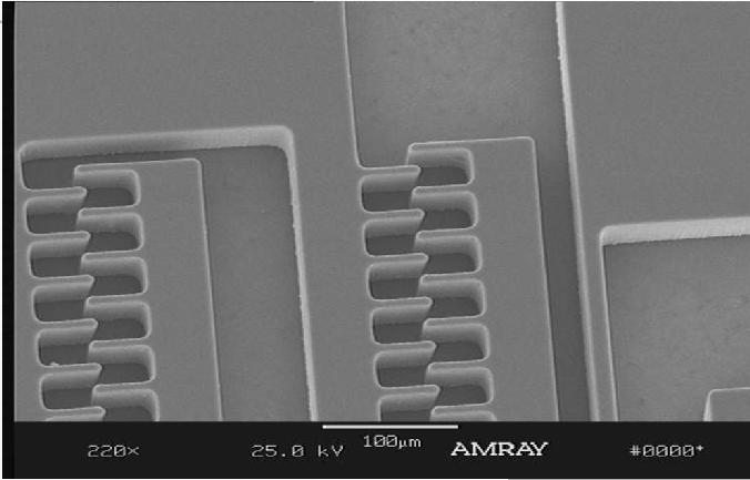
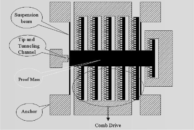
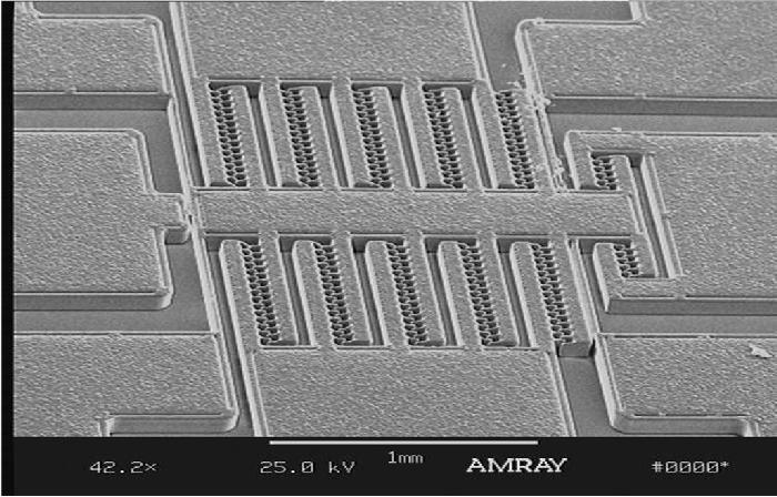
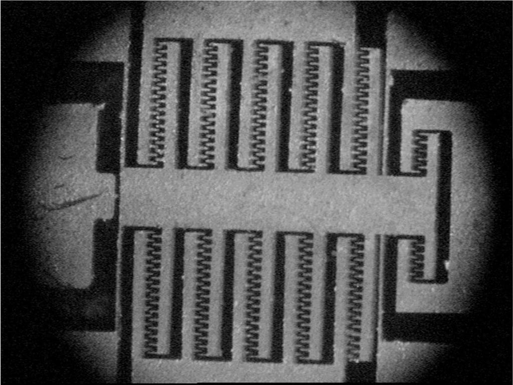
28 Comb Structure and Micro Tip

29 Hot Embossing Process
30 Movie
Soft Lithography: MIMIC. Micro Contact Printing. Microtransfer Molding. Soft Lithography: Replica Molding. Soft Lithography.
 Can We Measure Everything? Microfabrication Using Polymers Dr. Bruce K. Gale ENGR 494C and 594C Polymers for Microfabrication Examples diverse PDMS PMMA Polyurethane Polyimide Polystyrene Disadvantages
Outline. Introduction to the LIGA Microfabrication Process. What is LIGA? The LIGA Process. Dr. Bruce K. Gale Fundamentals of Microfabrication
 Outline Introduction to the LIGA Microfabrication Process Dr. Bruce K. Gale Fundamentals of Microfabrication What is LIGA? The LIGA Process Lithography Techniques Electroforming Mold Fabrication Analyzing
Microfabrication Using Silicon Mold Inserts and Hot Embossing
 Microfabrication Using Silicon Mold Inserts and Hot Embossing Liwei Lid), Chun-Jung Chiu'), Walter Bache?) and Mathias Heckele2) ')Institute of Applied Mechanics, National Taiwan University, Taipei, 106,
Mass Fabrication of Microstructured Parts with SR - Requirements to Throughput, Cost, and Quality
 Mass Fabrication of Microstructured Parts with SR - Requirements to Throughput, Cost, and Quality Markus Arendt 1, Pascal Meyer 2, Joachim Schulz 2 1 ANKA Angströmquelle Karlsruhe GmbH, P.O. Box 36 40,
General Introduction to Microstructure Technology p. 1 What is Microstructure Technology? p. 1 From Microstructure Technology to Microsystems
 General Introduction to Microstructure Technology p. 1 What is Microstructure Technology? p. 1 From Microstructure Technology to Microsystems Technology p. 9 The Parallels to Microelectronics p. 15 The
D Eggenstein-Leopoldshafen, Germany 2 University of Karlsruhe (TH), Institute for Microstructure Technology (IMT),
, Institute for Microstructure Technology (IMT),") Sub-µ structured Lotus Surfaces Manufacturing M. Worgull 1, M. Heckele 1, T. Mappes 2, B. Matthis 1, G. Tosello 3, T. Metz 4, J. Gavillet 5, P. Koltay 4, H. N. Hansen 3 1 Forschungszentrum Karlsruhe (FZK),
Sub-µ structured Lotus Surfaces Manufacturing M. Worgull 1, M. Heckele 1, T. Mappes 2, B. Matthis 1, G. Tosello 3, T. Metz 4, J. Gavillet 5, P. Koltay 4, H. N. Hansen 3 1 Forschungszentrum Karlsruhe (FZK),
Polymer Microfabrication: Methods and Application
 Polymer Microfabrication: Methods and Application Institute for Applied Materials & Department of Microsystems Engineering (IMTEK) at University of Freiburg KIT University of the State of Baden-Wuerttemberg
Characterization of Friction during the Demolding of Microstructures Molded by Hot Embossing
 Characterization of Friction during the Demolding of Microstructures Molded by Hot Embossing M. Worgull, J.-F. Hétu*, K.K. Kabanemi*, M. Heckele Forschungszentrum Karlsruhe, Institut für Mikrostrukturtechnik,
FABRICATION OF SWTICHES ON POLYMER-BASED BY HOT EMBOSSING. Chao-Heng Chien, Hui-Min Yu,
 Stresa, Italy, 26-28 April 2006 FABRICATION OF SWTICHES ON POLYMER-BASED BY HOT EMBOSSING, Mechanical Engineering Department, Tatung University 40 Chung Shan N. Rd. Sec. 3 Taipei, Taiwan ABSTRACT In MEMS
Preface Preface to First Edition
 Contents Foreword Preface Preface to First Edition xiii xv xix CHAPTER 1 MEMS: A Technology from Lilliput 1 The Promise of Technology 1 What Are MEMS or MST? 2 What Is Micromachining? 3 Applications and
Micro and nano structuring of carbon based materials for micro injection moulding and hot embossing
 Micro and nano structuring of carbon based materials for micro injection moulding and hot embossing Victor Usov, Graham Cross, Neal O Hara, Declan Scanlan, Sander Paulen, Chris de Ruijter, Daniel Vlasveld,
MEMS Fabrication. Beyond Integrated Circuits. MEMS Basic Concepts
 MEMS Fabrication Beyond Integrated Circuits MEMS Basic Concepts Uses integrated circuit fabrication techniques to make mechanical as well as electrical components on a single chip. Small size 1µm 1mm Typically
Micromachining AMT 2505
 Micromachining AMT 2505 Shanmuga Raja.B (BVB0912004) Module leader : Mr. Raja Hussain Introduction Micromachining are inherently connected to the evolution of Micro Electro Mechanical Systems (MEMS). Decades
Fundamentals of Manufacturing. EXAM 2 Dec 6, 2008 Name Open Book, (~75 min.) You are allowed a 5x7 card, a calculator and a pencil. Show all work.
 You are allowed a 5x7 card, a calculator and a pencil. Show all work.") MEEN 3349 001 Fundamentals of Manufacturing EXAM 2 Dec 6, 2008 Name Open Book, (~75 min.) You are allowed a 5x7 card, a calculator and a pencil. Show all work. Select the best definition, some may be used
MEEN 3349 001 Fundamentals of Manufacturing EXAM 2 Dec 6, 2008 Name Open Book, (~75 min.) You are allowed a 5x7 card, a calculator and a pencil. Show all work. Select the best definition, some may be used
Bulk Material Micro-structuring and Surface Modifications
 Bulk Material Micro-structuring and Surface Modifications Micro-structuring mechanical electrical (EDM) chemical irradiation electrochemical Surface modification electrodeposition PVD/CVD Materials metals
A Novel Extrusion Microns Embossing Method of Polymer Film
 Modern Mechanical Engineering, 2012, 2, 35-40 http://dx.doi.org/10.4236/mme.2012.22005 Published Online May 2012 (http://www.scirp.org/journal/mme) A Novel Extrusion Microns Embossing Method of Polymer
Study on stress evolution in the cooling process of micro hot embossing
 Gomez et al. International Journal of Mechanical and Materials Engineering 2014, 9:20 ORIGINAL PAPER Open Access Study on stress evolution in the cooling process of micro hot embossing Juan A Gomez 1,
UV15: For Fabrication of Polymer Optical Waveguides
 CASE STUDY UV15: For Fabrication of Polymer Optical Waveguides Master Bond Inc. 154 Hobart Street, Hackensack, NJ 07601 USA Phone +1.201.343.8983 Fax +1.201.343.2132 main@masterbond.com CASE STUDY UV15:
Micro Fabrication : Soft Lithography
 Micro Fabrication : Soft Lithography Last Class: 1. Electrowetting on Dielectric (EWOD) 2. Setup in EWOD 3. Basic Manipulations : Mixing Splitting, Translation 4. Optoelectrowetting (OEW) Today s Contents:
Tutorial on Micro Electro Mechanical Systems (MEMS)
") Tutorial on Micro Electro Mechanical Systems (MEMS) Bruce Kim Department of Electrical, 1 ! What is MEMS! Why MEMS! Applications! MEMS Fabrication! MEMS Packaging! Conclusion MEMS 2 WHAT IS MEMS! MEMS
Tutorial on Micro Electro Mechanical Systems (MEMS) Bruce Kim Department of Electrical, 1 ! What is MEMS! Why MEMS! Applications! MEMS Fabrication! MEMS Packaging! Conclusion MEMS 2 WHAT IS MEMS! MEMS
Micro Injection Molding of Micro Fluidic Platform
 Micro Injection Molding of Micro Fluidic Platform S. C. Chen, J. A. Chang, Y. J. Chang and S. W. Chau Department of Mechanical Engineering, Chung Yuan University, Taiwan, ROC Abstract In this study, micro
Nanoimprinting in Polymers and Applications in Cell Studies. Albert F. YEE Chemical Engineering & Materials Science UC Irvine
 Nanoimprinting in Polymers and Applications in Cell Studies Albert F. YEE Chemical Engineering & Materials Science UC Irvine Presentation outline Motivation Reversal imprinting Soft inkpad imprinting on
Laser-assisted chemical micromachining of metals and alloys
 RIKEN Review No. 43 (January, 2002): Focused on 2nd International Symposium on Laser Precision Microfabrication (LPM 2001) Laser-assisted chemical micromachining of metals and alloys Andreas Stephen, Thorsten
Precision Electroforming in High-Strength NiColoy
 Taking the Stress out of Electroforming www.nicoform.com Precision Electroforming in High-Strength NiColoy Copyright 2007 NiCoForm, Inc. (Rochester, NY) Electroforming What is it? What is it good for?
Manufacturing Technologies for MEMS and SMART SENSORS
 4 Manufacturing Technologies for MEMS and SMART SENSORS Dr. H. K. Verma Distinguished Professor (EEE) Sharda University, Greater Noida (Formerly: Deputy Director and Professor of Instrumentation Indian
Fabrication Technology, Part II
 EEL5225: Principles of MEMS Transducers (Fall 2003) Fabrication Technology, Part II Agenda: Process Examples TI Micromirror fabrication process SCREAM CMOS-MEMS processes Wafer Bonding LIGA Reading: Senturia,
Today s Class. Materials for MEMS
 Lecture 2: VLSI-based Fabrication for MEMS: Fundamentals Prasanna S. Gandhi Assistant Professor, Department of Mechanical Engineering, Indian Institute of Technology, Bombay, Recap: Last Class What is
Micro powder-injection moulding of metals and ceramics
 Sādhanā Vol.28,Parts1&2, February/April 2003, pp. 299 306. Printed in India Micro powder-injection moulding of metals and ceramics VOLKER PIOTTER, THOMAS GIETZELT and LOTHAR MERZ Forschungszentrum Karlsruhe
Surface Micromachining
 Surface Micromachining Micro Actuators, Sensors, Systems Group University of Illinois at Urbana-Champaign Outline Definition of surface micromachining Most common surface micromachining materials - polysilicon
Thin. Smooth. Diamond.
 UNCD Wafers Thin. Smooth. Diamond. UNCD Wafers - A Family of Diamond Material UNCD is Advanced Diamond Technologies (ADT) brand name for a family of thin fi lm diamond products. UNCD Aqua The Aqua series
Lecture 6. Through-Wafer Interconnect. Agenda: Through-wafer Interconnect Polymer MEMS. Through-Wafer Interconnect -1. Through-Wafer Interconnect -2
 Agenda: EEL6935 Advanced MEMS (Spring 2005) Instructor: Dr. Huikai Xie Lecture 6 Through-wafer Interconnect EEL6935 Advanced MEMS 2005 H. Xie 1/21/2005 1 Motivations: Wafer-level packaging CMOS 3D Integration
Thin. Smooth. Diamond.
 UNCD Wafers Thin. Smooth. Diamond. UNCD Wafers - A Family of Diamond Material UNCD is Advanced Diamond Technologies (ADT) brand name for a family of thin fi lm diamond products. UNCD Aqua The Aqua series
AML. AML- Technical Benefits. 4 Sept Wafer Bonding Machines & Services MEMS, IC, III-Vs.
 AML AML- Technical Benefits 4 Sept 2012 www.aml.co.uk AML In-situ Aligner Wafer Bonders Wafer bonding capabilities:- Anodic Bonding Si-Glass Direct Bonding e.g. Si-Si Glass Frit Bonding Eutectic Bonding
4. Process Integration: Case Studies
 Case Study #2: FCantilevered Microgripper Surface Machined MEMS Case Study #2: FCantilevered Microgripper Sandia Lucent Sandia Integrated Accelerometers Optomechanical Systems Integrated Sensors 1 Bulk
Vacuum casting, a new answer for manufacturing biomicrosystems
 1 Vacuum casting, a new answer for manufacturing biomicrosystems M Denoual 1 *, P Mognol 2, and B Lepioufle 1 1 Biomis-SATIE ENS-Cachan antenne de Bretagne, Bruz, France 2 IRCCyN Nantes, France The manuscript
Polymer-based Microfabrication
 Polymer-based Microfabrication PDMS SU-8 PMMA Hydrogel 1 Soft Lithography Developed by Whitesides, et. al A set of techniques for microfabrication based on the use of lithography, soft substrate materials
Applications of LIGA on Micro-punching Process for Metallic Materials
 Materials Science Forum Vols. 505-507 (2006) pp. 55-60 online at http://www.scientific.net (2006) Trans Tech Publications, Switzerland Applications of LIGA on Micro-punching Process for Metallic Materials
"Beyond Silicon," Feature Article, July beyond silicon
 Page 1 of 13 FEATURE FOCUS: Next-Generation Materials beyond silicon Engineers are expanding their material world to reduce the cost and tailor performance of microdevices. by John DeGaspari, Associate
ME 189 Microsystems Design and Manufacture. Chapter 9. Micromanufacturing
 ME 189 Microsystems Design and Manufacture Chapter 9 Micromanufacturing This chapter will offer an overview of the application of the various fabrication techniques described in Chapter 8 in the manufacturing
Thin Films: Sputtering Systems (Jaeger Ch 6 & Ruska Ch 7,) Can deposit any material on any substrate (in principal) Start with pumping down to high
 Can deposit any material on any substrate (in principal) Start with pumping down to high") Thin Films: Sputtering Systems (Jaeger Ch 6 & Ruska Ch 7,) Can deposit any material on any substrate (in principal) Start with pumping down to high vacuum ~10-7 torr Removes residual gases eg oxygen from
Thin Films: Sputtering Systems (Jaeger Ch 6 & Ruska Ch 7,) Can deposit any material on any substrate (in principal) Start with pumping down to high vacuum ~10-7 torr Removes residual gases eg oxygen from
ULTRAPRECISION MICROMACHINING OF MICROFLUIDIC DEVICES BY USE OF A HIGH-SPEED AIRBEARING SPINDLE
 ULTRAPRECISION MICROMACHINING OF MICROFLUIDIC DEVICES BY USE OF A HIGH-SPEED AIRBEARING SPINDLE Chunhe Zhang 1, Allen Y. Yi 1, Lei Li 1, L. James Lee 1, R. Ryan Vallance 2, Eric Marsh 3 1 The Ohio State
Soft Fabrication and Polymers
 Introduction to BioMEMS & Medical Microdevices Soft Fabrication and Polymers Companion lecture to the textbook: Fundamentals of BioMEMS and Medical Microdevices, by Prof., http://saliterman.umn.edu/ R012408
Holographix LLC Overview. High quality custom replicated optics and surface relief patterns in production volumes
 Holographix LLC Overview 2018 High quality custom replicated optics and surface relief patterns in production volumes One location in Marlborough, MA. 15,000 sq. ft. facility with additional space available
Thin Films: Sputtering Systems (Jaeger Ch 6 & Ruska Ch 7,) Sputtering: gas plasma transfers atoms from target to substrate Can deposit any material
 Sputtering: gas plasma transfers atoms from target to substrate Can deposit any material") Thin Films: Sputtering Systems (Jaeger Ch 6 & Ruska Ch 7,) Sputtering: gas plasma transfers atoms from target to substrate Can deposit any material on any substrate (in principal) Start with pumping down
Thin Films: Sputtering Systems (Jaeger Ch 6 & Ruska Ch 7,) Sputtering: gas plasma transfers atoms from target to substrate Can deposit any material on any substrate (in principal) Start with pumping down
Soft Lithography. Jin-Goo Park. Materials and Chemical Engineering Hanyang University, Ansan. Electronic Materials and Processing Lab.
 Hanyang University Soft Lithography Jin-Goo Park Materials and Chemical Engineering Hanyang University, Ansan Electronic Materials and Processing Lab. Introduction to Soft Lithography Research Micro- Electro-
Alternative MicroFabrication and Applications in Medicine and Biology
 Alternative MicroFabrication and Applications in Medicine and Biology Massachusetts Institute of Technology 6.152 - Lecture 15 Fall 2003 These slides prepared by Dr. Hang Lu Outline of Today s Materials
High Throughput Laser Processing of Guide Plates for Vertical Probe Cards Rouzbeh Sarrafi, Dana Sercel, Sean Dennigan, Joshua Stearns, Marco Mendes
 High Throughput Laser Processing of Guide Plates for Vertical Probe Cards Rouzbeh Sarrafi, Dana Sercel, Sean Dennigan, Joshua Stearns, Marco Mendes IPG Photonics - Microsystems Division Outline Introduction
DIE RECONFIGURATION AND RESTORATION USING LASER-BASED DEPOSITION. T.W. Skszek and M. T. J. Lowney. Abstract. DMD Process Overview
 DIE RECONFIGURATION AND RESTORATION USING LASER-BASED DEPOSITION T.W. Skszek and M. T. J. Lowney Abstract POM Company, Inc., located in Plymouth, Mich., has successfully commercialized the laser-based,
Silicon and Non-Silicon Materials for BioMEMS Fabrication
 Silicon and Non-Silicon Materials for BioMEMS Fabrication M. Gheorghe, M. Dinca, P. Galvin* * Tyndall National Institute, Cork, Ireland maringhe@tyndall.ie Short presentation of the Tyndall National Institute,
Micro-Nano Fabrication Research
 Micro-Nano Fabrication Research Technical Education Quality Improvement Programme 22-23 December 2014 Dr. Rakesh G. Mote Assistant Professor Department of Mechanical Engineering IIT Bombay rakesh.mote@iitb.ac.in;
Applications of High-Performance MEMS Pressure Sensors Based on Dissolved Wafer Process
 Applications of High-Performance MEMS Pressure Sensors Based on Dissolved Wafer Process Srinivas Tadigadapa and Sonbol Massoud-Ansari Integrated Sensing Systems (ISSYS) Inc., 387 Airport Industrial Drive,
Analysis of micro-structuring polymer replication by micro-injection moulding and hot embossing
 4M2007 Conference on Multi-Material Micro Manufacture 3-5 October 2007 Borovets Bulgaria Analysis of micro-structuring polymer replication by micro-injection moulding and hot embossing M. Sahli, C. Millot,
GLM General information. Technical Datasheet
 GLM 2060 Nanocomposite SU-8-negative tone photo-epoxy for layers from 6.0 to 50µm Technical Datasheet Gersteltec Sarl. Générale Guisan 26, 1009, Pully Switzerland Switzerland / Israel / Taiwan Contact:
Laser Micromachining for Industrial Applications and R&D. 3D-Micromac AG. Symposium on Smart Integrated Systems in Chemnitz. 3D-Micromac AG
 3D-Micromac AG Symposium on Smart Integrated Systems in Chemnitz 1 1 microdice - TLS-Dicing for separation of SiC 2 microprep - for high-throughput microstructure diagnostics 3 About 3D-Micromac AG 2 microdice
Evaluation of surface roughness and geometrical characteristic of additive manufacturing inserts for precision injection moulding
 Downloaded from orbit.dtu.dk on: Sep 29, 2018 Evaluation of surface roughness and geometrical characteristic of additive manufacturing inserts for precision injection moulding Davoudinejad, Ali; Charalambis,
LINE CARD. 877 No1 REPS. toll free : RepExact, LLC. 417 Second Street Annapolis, MD USA
 PRECISION COMPONENTS FOR MEDICAL AND LIFE SCIENCES LINE CARD 877 No1 REPS toll free : 877-661- 7377 Britt Manufacturing Co. (USA) ISO 13485 certified MIM/CIM Metal and Ceramics Powder Injection Molder.
Evolution of MEMS Technology
 Evolution of MEMS Technology 1 Raksha Sahadev Hukkeri, 2 Shreya Madapurmath, 3 Shreelekha Navale 1,2,3 UG Student, Department of ECE, SDMCET Dharwad Abstract Micro-Electro-Mechanical Systems (MEMS) is
Copyright Notice. HCL Technologies Ltd. All rights reserved. A DEFINITIVE GUIDE TO DESIGN FOR MANUFACTURING SUCCESS
 Title Subtitle Copyright Notice HCL Technologies Ltd. All rights reserved. No part of this document (whether in hardcopy or electronic form) may be reproduced, stored in a retrieval system, or transmitted,
Injection Moulding and Heat Treatment of Ni-Cr-Si-B Alloy Powder
 Injection Moulding and Heat Treatment of Ni-Cr-Si-B Alloy Powder M. Y. Anwar 1, M. Ajmal 1, M. T. Z. Butt 2 and M. Zubair 1 1. Department of Met. & Materials Engineering, UET Lahore. 2. Faculty of Engineering
MATERIALS. Silicon Wafers... J 04 J 01. MATERIALS / Inorganics & thin films guide
 J MATERIALS SUBSTRATES Silicon Wafers... J 04 J J 01 MATERIALS SUBSTRATES NEYCO has a complete range of crystal substrates for a wide variety of applications, including Semiconductor, Biotechnology, Nanotechnology,
FABRICATION ENGINEERING MICRO- NANOSCALE ATTHE AND. Fourth Edition STEPHEN A. CAMPBELL. of Minnesota. University OXFORD UNIVERSITY PRESS
 AND FABRICATION ENGINEERING ATTHE MICRO- NANOSCALE Fourth Edition STEPHEN A. CAMPBELL University of Minnesota New York Oxford OXFORD UNIVERSITY PRESS CONTENTS Preface xiii prrt i OVERVIEW AND MATERIALS
Advanced Manufacturing Choices
 Advanced Manufacturing Choices Table of Content Mechanical Removing Techniques Ultrasonic Machining (USM) Sputtering and Focused Ion Beam Milling (FIB) Ultrasonic Machining In ultrasonic machining (USM),
m-mold SHAPE DEPOSITION MANUFACTURING OF CERAMIC PARTS
 m-mold SHAPE DEPOSITION MANUFACTURING OF CERAMIC PARTS S.W. NAM, J. STAMPFL, H.C. LIU, S. KANG, F. B. PRINZ Rapid Prototyping Laboratory, Building 530, Room 226, Stanford University, Stanford CA 94305,
Advanced Polymers And Resists For Nanoimprint Lithography
 Q U A L I T Y A S S U R A N C E MICROSYSTEMS & NANOSYSTEMS SPECIAL REPORT Advanced Polymers And Resists For Nanoimprint Lithography Numerous polymer systems specifically designed for nanoimprint lithography
Meso A/SMP Approach. Abstract
 Abstract Additive/Subtractive Material Processing for Mesoscopic Parts Yih-Lin Cheng, Jurgen Stampfl, Rudolf Leitgeb, and Fritz B. Prinz Stanford University, Stanford, CA Mesoscopic additive/subtractive
3D Laser Lithography in Biotechnology and Medical Technology
 3D Laser Lithography in Biotechnology and Medical Technology High-Precision, Piezo-Based Nanopositioning Systems Advance Technology Page 1 of 6 Laser technology makes it possible to create even very complex
Metal extrusion. Metal stamping
 Metal extrusion Answer the following questions 1. In which of the following extrusion operation is friction a factor in determining the extrusion force (one best answer): (a) direct extrusion or (b) indirect
LASER MICROMACHINING A New Tool for Precision Engineers
 LASER MICROMACHINING A New Tool for Precision Engineers Nadeem Rizvi UK Laser Micromachining Centre Laser Applications for Micro and Nano Engineering AILU Workshop 14 June 2006 (Oxford) FOCUS ON MICRO
Fall 2008 EE 410/510: Microfabrication and Semiconductor Processes M W 12:45 PM 2:20 PM EB 239 Engineering Bldg.
 Fall 2008 EE 410/510: Microfabrication and Semiconductor Processes M W 12:45 PM 2:20 PM EB 239 Engineering Bldg. Instructor: John D. Williams, Ph.D. Assistant Professor of Electrical and Computer Engineering
Surface Micromachining
 Surface Micromachining Outline Introduction Material often used in surface micromachining Material selection criteria in surface micromachining Case study: Fabrication of electrostatic motor Major issues
Enabling Technology in Thin Wafer Dicing
 Enabling Technology in Thin Wafer Dicing Jeroen van Borkulo, Rogier Evertsen, Rene Hendriks, ALSI, platinawerf 2G, 6641TL Beuningen Netherlands Abstract Driven by IC packaging and performance requirements,
TSV Processing and Wafer Stacking. Kathy Cook and Maggie Zoberbier, 3D Business Development
 TSV Processing and Wafer Stacking Kathy Cook and Maggie Zoberbier, 3D Business Development Outline Why 3D Integration? TSV Process Variations Lithography Process Results Stacking Technology Wafer Bonding
Thermal Spray Coatings in Severe Service Elaine Motyka 3/2/2017
 Thermal Spray Coatings in Severe Service Elaine Motyka 3/2/2017 In this session Basics of Thermal Spray Coatings Defining Thermal Spray Common processes Coating microstructures Properties affected by process
Laser Micromilling :
 Laser Micromilling : An Enabling Technology for MicroComponent Replication Martyn Knowles Oxford Lasers Ltd. Unit 8, Moorbrook Park Didcot, Oxon OX11 7HP Tel: +44-1235-814433 Outline Introduction Process
Lithography Independent Fabrication of Nano-MOS-Transistors with W = 25 nm and L = 25 nm
 Lithography Independent Fabrication of Nano-MOS-Transistors with W = 25 nm and L = 25 nm J. T. Horstmann John_Horstmann@ieee.org C. Horst Christian.Horst@udo.edu K. F. Goser goser@ieee.org Abstract The
FULL-DENSIFICATION OF SLS PARTS BY RE-MELTING. Abstract
 FULL-DENSIFICATION OF SLS PARTS BY RE-MELTING T. NIINO and H. YAMADA Institute of Industrial Science, The University of Tokyo 4-6-1 Komaba Meguro Tokyo, 153-8505 Japan Reviewed, accepted August 4, 2004
Chapter 7 Evaluation of Injection-Molding Phenomena Part 1: Measurement of temperature distribution in the molded materials
 Chapter 7 Evaluation of Injection-Molding Phenomena Part 1: Measurement of temperature distribution in the molded materials 1. Evaluation of Injection-Molding Phenomena It is effective to evaluate the
Mikrosensorer. Microfabrication 1
 Mikrosensorer Microfabrication 1 Literature Introductory MEMS Fabrication and Applications Thomas M. Adams and Richard A. Layton Available as ebook on http://www.lub.lu.se/en/search/lubsearch.html This
SINGLE CRYSTAL SAPPHIRE
 SINGLE CRYSTAL SAPPHIRE Single Crystal Sapphire plays an everincreasingly important role as a material for high reliability Opto-Electronics today due to excellent mechanical characteristics, chemical
Micro-Electro-Mechanical Systems (MEMS) Fabrication. Special Process Modules for MEMS. Principle of Sensing and Actuation
 Fabrication. Special Process Modules for MEMS. Principle of Sensing and Actuation") Micro-Electro-Mechanical Systems (MEMS) Fabrication Fabrication Considerations Stress-Strain, Thin-film Stress, Stiction Special Process Modules for MEMS Bonding, Cavity Sealing, Deep RIE, Spatial forming
Micro-Electro-Mechanical Systems (MEMS) Fabrication Fabrication Considerations Stress-Strain, Thin-film Stress, Stiction Special Process Modules for MEMS Bonding, Cavity Sealing, Deep RIE, Spatial forming
Micromachining vs. Soft Fabrication
 Introduction to BioMEMS & Medical Microdevices Silicon Microfabrication Part 1 Companion lecture to the textbook: Fundamentals of BioMEMS and Medical Microdevices, by Prof., http://saliterman.umn.edu/
Dr. M. Medraj Mech. Eng. Dept. - Concordia University Mech 421/6511 lecture 12/2
 POWDER METALLURGY Characterization of Engineering Powders Production of Metallic Powders Conventional Pressing and Sintering Alternative Pressing and Sintering Techniques Materials and Products for PM
MEMS technology for production of different micro- and nanodevices
 P6.4 MEMS technology for production of different micro- and nanodevices A.M. Kudanovich, N.I. Mukhurov, L.R. Paleuskaya, Y.V. Mironchyk Laboratory of Micro- Electronics, Mechanics and Sensorics, Institute
Laboratory-Platen-Presses Types P/M
 Laboratory-Platen-Presses Types P/M Laboratory machines for the processing of polymers Collin laboratory platen presses offer Uniform temperature distribution over the platen surface Maximum heating/cooling
LASER MICROFABRICATION OF MULTIFUNCTIONAL DEVICES
 LASER MICROFABRICATION OF MULTIFUNCTIONAL DEVICES Andy Goater, Gary Owen, Julian Burt & Nadeem Rizvi UK Laser Micromachining Centre Laser Microprocessing of Challenging Materials and Architectures AILU
Laser Machining Processes Laser heat processing divided into 3 regions Heating Melting Vaporization
 Laser Machining Processes Laser heat processing divided into 3 regions Heating Melting Vaporization Laser Surface Treatment Annealing or Transformation Hardening Surface hardness Surface Melting Homogenization,
An intro to Liquidmetal
 An intro to Liquidmetal Challenging parts an example Manufacturing metal parts often leads to obstacles A common example is precision assemblies that closely fit together Devices often go into the body,
II. A. Basic Concept of Package.
 Wafer Level Package for Image Sensor Module Won Kyu Jeung, Chang Hyun Lim, Jingli Yuan, Seung Wook Park Samsung Electro-Mechanics Co., LTD 314, Maetan3-Dong, Yeongtong-Gu, Suwon, Gyunggi-Do, Korea 440-743
Combinatorial Multilevel Mold Insert Using Micromachining and X-ray Lithography
 Summary Combinatorial Multilevel Mold Insert Using Micromachining and X-ray Lithography V. Singh 1, J. Goettert 1, O. Jinka 1,2,* 1 Center for Advanced Microstructures and Devices (CAMD) 2 Mechanical Engineering,
Three-Dimensional Laser Writing on the Nanometer Scale
 Three-Dimensional Laser Writing on the Nanometer Scale Piezo Drives are Driving Technology Forward Page 1 of 5 The best possible positioning accuracy is now mandatory in many fields of application. The
KrF Excimer Laser Micromachining of Silicon for Micro- Cantilever Applications
 OPEN ACCESS Conference Proceedings Paper Sensors and Applications www.mdpi.com/journal/sensors KrF Excimer Laser Micromachining of Silicon for Micro- Cantilever Applications A.F.M. Anuar 1*, Y. Wahab,
A simple method for microlens fabrication by the modified LIGA process
 INSTITUTE OF PHYSICS PUBLISHING JOURNAL OF MICROMECHANICS AND MICROENGINEERING J. Micromech. Microeng. 12 (22) 334 34 PII: S96-1317(2)3292-6 A simple method for microlens fabrication by the modified LIGA
GE Sensing & Inspection Technologies MEMS. Global Solutions for Microsystems
 GE Sensing & Inspection Technologies MEMS Global Solutions for Microsystems g Global research, development and manufacturing excellence Groby, United Kingdom MEMS Design and Manufacturing Center Advanced
Laser Surface Melting Want to melt the surface locally Melt & rapid solidification get fine homogeneous structures (recrystallize) Little thermal
 Little thermal") Laser Surface Melting Want to melt the surface locally Melt & rapid solidification get fine homogeneous structures (recrystallize) Little thermal penetration thus small thermal distortion for sensitive
Laser Surface Melting Want to melt the surface locally Melt & rapid solidification get fine homogeneous structures (recrystallize) Little thermal penetration thus small thermal distortion for sensitive
A discussion of crystal growth, lithography, etching, doping, and device structures is presented in
 Chapter 5 PROCESSING OF DEVICES A discussion of crystal growth, lithography, etching, doping, and device structures is presented in the following overview gures. SEMICONDUCTOR DEVICE PROCESSING: AN OVERVIEW
Solid State Sensors. Microfabrication 8/22/08 and 8/25/08
 Solid State Sensors Microfabrication 8/22/08 and 8/25/08 Purpose of This Material To introduce the student to microfabrication techniques as used to fabricate MEMS Sensors Understand concepts not specifics
Thermal Nanoimprinting Basics
 Thermal Nanoimprinting Basics Nanoimprinting is a way to replicate nanoscale features on one surface into another, like stamping copies are made by traditional fabrication techniques (optical/ebeam lith)
Cost Effective 3D Glass Microfabrication for Advanced Packaging Applications
 Cost Effective 3D Glass Microfabrication for Advanced Packaging Applications Authors: Jeb. H Flemming, Kevin Dunn, James Gouker, Carrie Schmidt, Roger Cook ABSTRACT Historically, while glasses have many
We get small. Micron-scale Circuits and Structures from Prototype through Production
 We get small. Micron-scale Circuits and Structures from Prototype through Production Smaller, tighter, better. When you need to produce ultra-small electrical, mechanical and optical components to extreme
Plasma Etching Rates & Gases Gas ratios affects etch rate & etch ratios to resist/substrate
 Plasma Etching Rates & Gases Gas ratios affects etch rate & etch ratios to resist/substrate Development of Sidewalls Passivating Films Sidewalls get inert species deposited on them with plasma etch Creates