Spectrometer gratings based on direct-write e-beam lithography
|
|
|
- Tiffany McKenzie
- 5 years ago
- Views:
Transcription


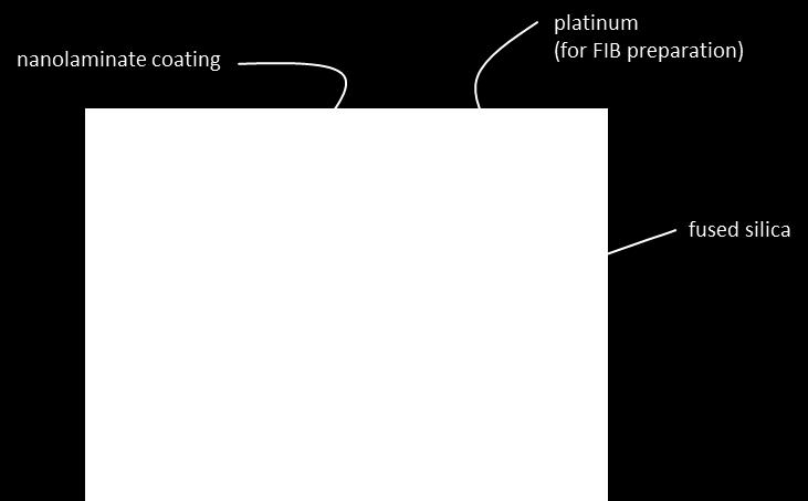
1 Spectrometer gratings based on direct-write e-beam lithography U.D. Zeitner, T. Flügel-Paul, T. Harzendorf, M. Heusinger, E.-B. Kley Fraunhofer Institut für Angewandte Optik und Feinmechanik Jena, Germany 10. October 2017 Electron-beam lithography for grating fabrication Examples of astro-gratings: CUBES UV-transmission grating CarbonSat high-resolution gratings Sub- structures for ultra-wide-band gratings 3µm

 compressed Pulse chirped Pulse relevant")

2 High Performance Applications of Gratings Spectrometers for Astronomy and Earth Observation Manipulation/Compression of Ultra-Short Laser Pulses Sentinel 4 (ESA) compressed Pulse chirped Pulse relevant parameters: spectral dispersion bandwidth efficiency / polarization wavefront straylight size, often extreme demands to obtain required performance
3 Grating Technology at the IOF 1. Resist exposure with e-beam lithography 2. Resist development e - resist Cr-layer SiO 2 -Substrate 3. Chromium etching (RIE) 4. Deep etching into substrate (ICP) 5. Removal of Cr-layer optional: multiple iterations of the process for multi-level elements


4 Gratings on dielectric layer stacks -1 st order 0 th order grating HR layer stack substrate 1µm highly efficient reflection gratings transmission gratings with tailored polarization properties
: <50nm address grid: 1nm stitching error: < 12nm")

5 The Vistec SB350 OS e-beam writer max. writing field: 300mm x 300mm max. substrate thickness: 15mm resolution (direct write): <50nm address grid: 1nm stitching error: < 12nm P-V / < 2.2nm RMS placement error: < 14nm P-V writing strategy: variable shaped beam / cell projection huge flexibility to tailor the structure parameters! e-beam angular apertures electron optics very fast writing process! SB350 OS (Vistec)
![period variation [pm] 50mm Key Performance: Writing Accuracy wave-front measurement (1µm period grating + technology, Littrow-Mount) 19mm + 6.3nm wavefront - 6.6nm placement PV 12.8nm <10.](/docs-images/82/86254368/images/6-2.jpg "3 nm rms 1.4nm <1.")
6 period variation [pm] 50mm Key Performance: Writing Accuracy wave-front measurement (1µm period grating + technology, Littrow-Mount) 19mm + 6.3nm wavefront - 6.6nm placement PV 12.8nm <10.3 nm rms 1.4nm <1.1 nm Applications requiring this accuracy position [mm] period variation < 5 pm - Asphere-Test CGH - Puls compression gratings - Spectrometer gratings (space application)


![[sr -1 ] 10 0 10-1 optimized writing process significant reduction of](/docs-images/82/86254368/images/7-6.jpg "peak number and intensity 10-2 0 2 4 6 8 10 angle wrt.")
7 Accuracy of writing process: straylight BSDF of -1 st DO: Optimization of e-beam writing process sr conventional e-beam #22 8Pass, Std I reflex from FIMAS_uze147e_3 writing process Wein-Formula with =2nm substrate 10 1 FIMAS EBB BSDF [sr -1 ] optimized writing process significant reduction of peak number and intensity angle wrt. -1 st diffraction order [ ]
8 Examples of realized spectrometer gratings
9 CUBES UV Transmission Grating CUBES (Cassegrain U-Band Brazilian ESO-Spectrograph Requirements: spectral band: 300nm 400nm line density: 3448 lines/mm p=290nm AOI: 31 grating size: 250 x 250 mm² ; mosaic of 2x [250mm x 130mm] Challenges: commercial VPH gratings difficult in the UV Solution: Binary fused silica gratings
![526nm efficiency [%] 706nm](/docs-images/82/86254368/images/10-5.jpg "efficiency [%] ESO Cubes")


10 526nm efficiency [%] 706nm efficiency [%] ESO Cubes Spectrometer Grating parameters: wavelength: 300nm nm period: 290nm SiO 2 -option: 100nm ALD-option: Al 2 O 3 221nm

11 Atomic-Layer-Deposition (ALD) precursor pulse 1 ALD-layer purge repeat ALD cycles N times purge precursor pulse 2 1µm surface activated chemical reactions conformal overcoating of surface reliefs large number of materials possible, e.g. TiO 2, Ta 2 O 5, Al 2 O 3, HfO 2

12 CUBES UV Transmission Grating design best fit of measurement data realized grating during efficiency measurement grating size: 250mm x 130mm


13 Tiling for Larger Gratings single grating 210mm x 210mm active alignment for wave-front optimization also possible for transmission gratings arrangement of 2 reflection gratings (420mm x 210mm)
 mean angle of diffraction 63.6 55.5 Transmission Gratings in -1. order Littrow configuration Angular dispersion 0.3 / nm 0.1 /nm polarization avg.")
14 Carbon Monitoring Satellite (CarbonSat) instrument concept: NIR SWIR-1 SWIR-2 Parameter NIR SWIR-1 747nm 1590nm wavelength 773nm 1675nm grating period 423nm 991nm angle of incidence to the grating (equivalent in air) mean angle of diffraction Transmission Gratings in -1. order Littrow configuration Angular dispersion 0.3 / nm 0.1 /nm polarization avg. efficiency >70% >70% polarization sensitivity <10% <10%
15 NIR High Resolution Transmission Grating

 coating to")
16 NIR High Resolution Transmission Grating use high-refractive-index (dielectric) coating to reduce depth
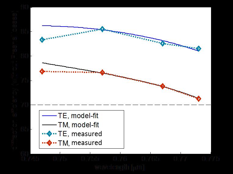

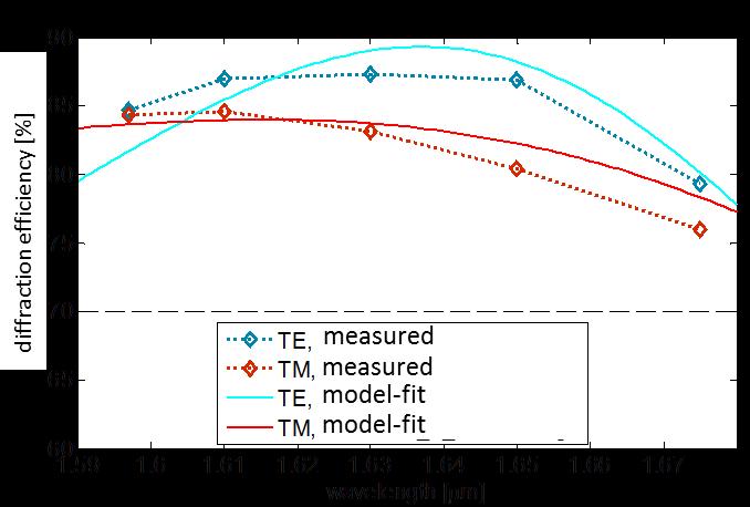
17 Optical Performance SWIR-1-grating NIR-grating AOI: 64 AOI: 55

18 Direct Glass-to-Glass Bonding Advantages: adhesive free glass-to-glass connection no additional optical interface achieved alignment accuracy: 0.25mrad (< 1 arcmin) bond strength up to 2/3 of bulk fused silica current TRL: 6
 80% 60% 40% 20% 0% 340 440 540 640 740 840 940 1040")
19 efficiency Wide-Band Gratings typical requirements for a low-resolution, broad-band disperser spectral range: several 100nm AOI: near-perpendicular incidence period: few µm Blaze-Grating 100% classical approach blazed-grating in low order (saw-tooth profile) 80% 60% 40% 20% 0% wavelength [nm]

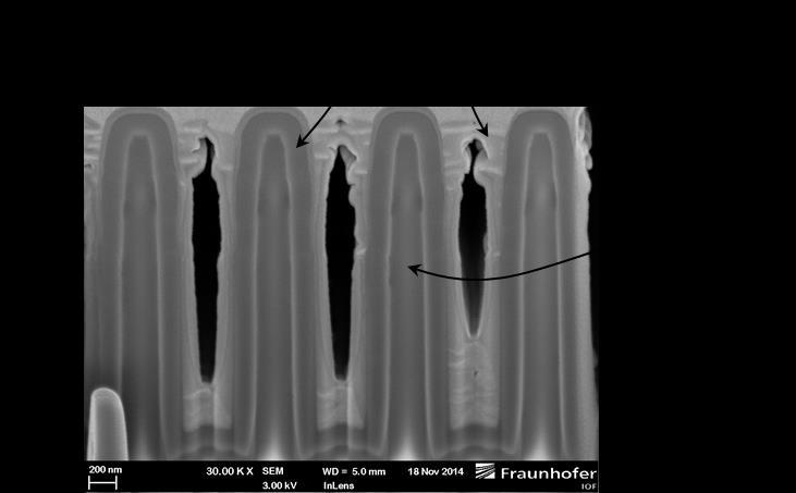
20 Echelle or Echellette Structures Electron Beam Lithography Ion Beam Etching of Mask Wet Chemical Etching of Silicon Blaze Angle can be adjusted by crystalline orientation of Silicon substrate


21 Echelle or Echellette Structures period = 30µm period = 2µm also lower line densities possible currently shown on 6 size substrates (up to 12 possible) integrated crossdispersion grating by direct-write structuring

22 Alternative: Effective Index Gratings sub-wavelength pattern with varying fill factor blazed grating local effective index sub-wavelength structures = local fill-factor variation Ph. Lalanne et al Advantages: only one lithography step tailoring of dispersion properties

; [500nm")
![800nm] GAIA (global](/docs-images/82/86254368/images/23-6.jpg "astrometic")
;")
23 Effective Medium Gratings FLEX (fluorescence explorer); [500nm 800nm] GAIA (global astrometic interferometer for astrophysics); [750nm 800nm] top view grating period
 effective medium approach pillars air voids bulk aluminum side view top view SiO 2 TE diffraction eff.")
24 Wide-Band Reflection Grating typical requirements based on a concave grating spectral range: 340nm 1050nm AOI: 0.5 period: 30µm Al 2 O 3 (30nm) effective medium approach pillars air voids bulk aluminum side view top view SiO 2 TE diffraction eff. [%] wavelength [nm] 30µm

25 Wide-Band Reflection Grating realized by E-beam lithography measured diffraction efficiency: including reduced UV reflectivity of Al-layer very weak spectral dependency of diffraction efficiency

")


26 Summary Direct write electron-beam lithography has a huge potential for the realization of high-performance gratings It offers Sub-period a unique engineering flexibility and by combining the accuracy to meet even extreme E-Beam requirements lithography and Atomic-Layer-Deposition To make use of the large flexibility and the Atomic-Layer-Deposition advantageous optical properties (ALD) considerably requires talking extends with the flexibility the grating to access manufacturer the full potential already of during advanced the design grating of designs the instrument!!! (not after PDR ) L Realization of GRISMs by direct bonding Examples are: high resolution gratings with low polarization sensitivity echelle-type gratings with integrated cross-disperser ultra-wide-band gratings for lower resolution spectrometers L
Micro- and Nano-Technology... for Optics
 Micro- and Nano-Technology...... for Optics 3.2 Lithography U.D. Zeitner Fraunhofer Institut für Angewandte Optik und Feinmechanik Jena Electron Beam Column electron gun beam on/of control magnetic deflection
Low aberration monolithic diffraction gratings for high performance optical spectrometers
 Low aberration monolithic diffraction gratings for high performance optical spectrometers P. Triebel 1, T. Diehl 1, M. Burkhardt 2, L. Erdmann 2, A. Kalies 2,A. Pesch 2, A. Gatto 2 1 Carl Zeiss Spectroscopy
State of the art in silicon immersed gratings for space - Aaldert van Amerongen, Hélène Krol, Catherine Grèzes-Besset, Tonny Coppens, Ianjit Bhatti,
 State of the art in silicon immersed gratings for space - Aaldert van Amerongen, Hélène Krol, Catherine Grèzes-Besset, Tonny Coppens, Ianjit Bhatti, Dan Lobb, Bram Hardenbol, Ruud Hoogeveen Climate research
PATTERNING OF OXIDE THIN FILMS BY UV-LASER ABLATION
 Journal of Optoelectronics and Advanced Materials Vol. 7, No. 3, June 2005, p. 1191-1195 Invited lecture PATTERNING OF OXIDE THIN FILMS BY UV-LASER ABLATION J. Ihlemann * Laser-Laboratorium Göttingen e.v.,
Coatings. Ion Assisted Deposition (IAD) process Advance Plasma Source (APS) plasma-ion assisted Deposition. Coatings on Optical Fibers
 process Advance Plasma Source (APS) plasma-ion assisted Deposition. Coatings on Optical Fibers") Anti-Reflection Custom Ion Assisted Deposition (IAD) process Advance Plasma Source (APS) plasma-ion assisted Deposition Anti-Reflection on Optical Fibers OptoSigma supplies a wide selection of optical
Anti-Reflection Custom Ion Assisted Deposition (IAD) process Advance Plasma Source (APS) plasma-ion assisted Deposition Anti-Reflection on Optical Fibers OptoSigma supplies a wide selection of optical
Deep-etched fused silica grating as a (de)multiplexer for DWDM application at the wavelength of 1.55µm
multiplexer for DWDM application at the wavelength of 1.55µm") Deep-etched fused silica grating as a (de)multiplexer for DWDM application at the wavelength of 1.55µm Yanyan Zhang*, Changhe Zhou, Huayi Ru, Shunquan Wang Shanghai Institute of Optics and Fine Mechanics,
Deep-etched fused silica grating as a (de)multiplexer for DWDM application at the wavelength of 1.55µm Yanyan Zhang*, Changhe Zhou, Huayi Ru, Shunquan Wang Shanghai Institute of Optics and Fine Mechanics,
Photonics made in jena. Micro-Assembly and
 Photonics made in jena Fraunhofer Institute for Applied Optics and Precision Engineering Micro-Assembly and System Integration 2 www.iof.fraunhofer.com Solutions with Light Expertise in Optical System
Figure 6. Rare-gas atom-beam diffraction patterns. These results were obtained by Wieland Schöllkopf and Peter Toennies at the Max-Planck Institute
 Figure 6. Rare-gas atom-beam diffraction patterns. These results were obtained by Wieland Schöllkopf and Peter Toennies at the Max-Planck Institute in Göttingen, Germany, using a freestanding, 100nm-period
Deep-etched high-density fused-silica transmission gratings with high efficiency at a wavelength of 1550 nm
 Deep-etched high-density fused-silica transmission gratings with high efficiency at a wavelength of 1550 nm Shunquan Wang, Changhe Zhou, Yanyan Zhang, and Huayi Ru We describe the design, fabrication,
Properties of Inverse Opal Photonic Crystals Grown By Atomic Layer Deposition
 Properties of Inverse Opal Photonic Crystals Grown By Atomic Layer Deposition J.S. King 1, C. W. Neff 1, W. Park 2, D. Morton 3, E. Forsythe 3, S. Blomquist 3, and C. J. Summers 1 (1) School of Materials
At wavelength characterization of EUV and soft X-ray gratings
 At wavelength characterization of EUV and soft X-ray gratings F. Scholze, A, Haase, C. Laubis, V. Soltwisch, J. Wernecke, M. Krumrey Physikalisch-Technische Bundesanstalt, Abbestraße 2-12, 10587 Berlin,
Introduction to Lithography
 Introduction to Lithography G. D. Hutcheson, et al., Scientific American, 290, 76 (2004). Moore s Law Intel Co-Founder Gordon E. Moore Cramming More Components Onto Integrated Circuits Author: Gordon E.
PRECISION OPTICAL FILTERS BY EOSS - ENHANCED OPTICAL SPUTTERING SYSTEM. Fraunhofer
 PRECISION OPTICAL FILTERS BY EOSS - ENHANCED OPTICAL SPUTTERING SYSTEM EOSS ENHANCED OPTICAL SPUTTERING SYSTEM Fraunhofer IST, Braunschweig Contact: Dr. M. Vergöhl +49 531 2155 640 EOSS Coating System
NIR High-Efficiency Subwavelength DiEractive Structures In Semiconductors.
 c NIR High-Efficiency Subwavelength DiEractive Structures In Semiconductors. R.E. Smith, M.E. Warren, J.R. Wendt and G.A. Vawter Sandia National Laboratories Albuquerque, NM 87185-0603 Abstract: We have
Thin Film Micro-Optics
 Thin Film Micro-Optics New Frontiers of Spatio-Temporal Beam Shaping Ruediger Grunwald Max Born Institut for Nonlinear Optics and Short Pulse Spectroscopy Berlin, Germany ELSEVIER Amsterdam Boston Heidelberg
Optical Coatings. Photonics 4 Luxury Coatings , Genève. Dr. Andreas Bächli Head of Optical Coatings at RhySearch, Buchs (SG)
") Optical Coatings Photonics 4 Luxury Coatings 21.06.2017, Genève Dr. Andreas Bächli Head of Optical Coatings at RhySearch, Buchs (SG) RhySearch The Research- and Innovation Center in the Rhine Valley RhySearch
Optical Coatings Photonics 4 Luxury Coatings 21.06.2017, Genève Dr. Andreas Bächli Head of Optical Coatings at RhySearch, Buchs (SG) RhySearch The Research- and Innovation Center in the Rhine Valley RhySearch
EUV Transmission Lens Design and Manufacturing Method
 1 EUV Transmission Lens Design and Manufacturing Method Kenneth C. Johnson kjinnovation@earthlink.net 7/16/2018 http://vixra.org/abs/1807.0188 Abstract This paper outlines a design for an EUV transmission
Detectors and Coatings for Efficient Systems for Future UV Astronomy
 Detectors and Coatings for Efficient Systems for Future UV Astronomy John Hennessy M. E. Hoenk, A. Carver, T.J. Jones, A. Jewell, E. Hamden, T. Goodsall, S. Nikzad Jet Propulsion Laboratory, California
Manipulation and control of spatial ALD layers for flexible devices. Aimcal Memphis 2016; Edward Clerkx
 Manipulation and control of spatial ALD layers for flexible devices Meyer Burger Netherlands Equipment manufacturer Functional inkjet printing Based in Eindhoven, the Netherlands Part of world-wide Meyer
Single-digit-resolution nanopatterning with. extreme ultraviolet light for the 2.5 nm. technology node and beyond
 Electronic Supplementary Material (ESI) for Nanoscale. This journal is The Royal Society of Chemistry 205 Supplementary Information for: Single-digit-resolution nanopatterning with extreme ultraviolet
Characterisation of Fe-Ni amorphous thin films for possible magnetostrictive sensor applications
 Characterisation of Fe-Ni amorphous thin films for possible magnetostrictive sensor applications Contents 9.1 Introduction 9.2 Experiment 9.3 Results and Discussions 9.4 Conclusion 9.1 Introduction Magnetostrictive
Precision Optical Engineering
 Precision Optical Engineering Products: Prisms Windows Mirrors Flats and Master angles Sight Glasses Key Features: Prisms (Contacted, Cemented, AR coated, Mounted) Windows (Flat, wedged, curved, drilled,
In-situ laser-induced contamination monitoring using long-distance microscopy
 In-situ laser-induced contamination monitoring using long-distance microscopy Paul Wagner a, Helmut Schröder* a, Wolfgang Riede a a German Aerospace Center (DLR), Institute of Technical Physics, Pfaffenwaldring
EECS130 Integrated Circuit Devices
 EECS130 Integrated Circuit Devices Professor Ali Javey 9/13/2007 Fabrication Technology Lecture 1 Silicon Device Fabrication Technology Over 10 15 transistors (or 100,000 for every person in the world)
Investigation on High Efficiency Volume Bragg gratings performances for spectrometry in space environment
 Investigation on High Efficiency Volume Bragg gratings performances for spectrometry in space environment Jérôme Loicq, Y. Stockman, Marc Georges Centre spatial de Liège-University of Liège Liege, Belgium
Understanding Optical Coatings For Military Applications
 Understanding Optical Coatings For Military Applications By Trey Turner, Chief Technology Officer, REO Virtually all optical components used in military applications, such as target designation, rangefinding
ATOMIC LAYER DEPOSITION FOR PHOTONIC CRYSTAL DEVICES
 ATOMIC LAYER DEPOSITION FOR PHOTONIC CRYSTAL DEVICES E. Graugnard, J. S. King, D. Heineman, and C. J. Summers School of Materials Science and Engineering, Georgia Institute of Technology, Atlanta, GA,
ALD systems and SENTECH Instruments GmbH
 ALD systems and processes @ SENTECH Instruments GmbH H. Gargouri, F. Naumann, R. Rudolph and M. Arens SENTECH Instruments GmbH, Berlin www.sentech.de 1 2 Agenda 1. Company Introduction 2. SENTECH-ALD-Systems
EUV Transmission Lens Design and Manufacturing Method
 1 EUV Transmission Lens Design and Manufacturing Method Kenneth C. Johnson kjinnovation@earthlink.net 7/9/2018 Abstract This paper outlines a design for an EUV transmission lens comprising blazed, phase-
Compact hybrid plasmonic-si waveguide structures utilizing Albanova E-beam lithography system
 Compact hybrid plasmonic-si waveguide structures utilizing Albanova E-beam lithography system Introduction Xu Sun Laboratory of Photonics and Microwave Engineering, Royal Institute of Technology (KTH),
Dielectric II-VI and IV-VI Metal Chalcogenide Thin Films in Hollow Glass Waveguides (HGWs) for Infrared Spectroscopy and Laser Delivery
 for Infrared Spectroscopy and Laser Delivery") Dielectric II-VI and IV-VI Metal Chalcogenide Thin Films in Hollow Glass Waveguides (HGWs) for Infrared Spectroscopy and Laser Delivery Carlos M. Bledt * a, Daniel V. Kopp a, and James A. Harrington a
Dielectric II-VI and IV-VI Metal Chalcogenide Thin Films in Hollow Glass Waveguides (HGWs) for Infrared Spectroscopy and Laser Delivery Carlos M. Bledt * a, Daniel V. Kopp a, and James A. Harrington a
Solutions with Light. Energy and environment, Information and communication, Healthcare and medical technology, Safety and mobility.
 Fraunhofer Institute for Applied Optics and Precision Engineering Solutions with Light EXPERTISE in Optical system technology 2 Solutions with Light The Fraunhofer IOF conducts application oriented research
THIN METALLIC LAYERS STRUCTURED BY E-BEAM LITHOGRAPHY. Miroslav HORÁČEK, Vladimír KOLAŘÍK, Michal URBÁNEK, František MATĚJKA, Milan MATĚJKA
 THIN METALLIC LAYERS STRUCTURED BY E-BEAM LITHOGRAPHY Miroslav HORÁČEK, Vladimír KOLAŘÍK, Michal URBÁNEK, František MATĚJKA, Milan MATĚJKA Ústav přístrojové techniky AV ČR, v. v. i., Královopolská 147,
Lecture 5. SOI Micromachining. SOI MUMPs. SOI Micromachining. Silicon-on-Insulator Microstructures. Agenda:
 EEL6935 Advanced MEMS (Spring 2005) Instructor: Dr. Huikai Xie SOI Micromachining Agenda: SOI Micromachining SOI MUMPs Multi-level structures Lecture 5 Silicon-on-Insulator Microstructures Single-crystal
Supporting Information for
 Electronic Supplementary Material (ESI) for Nanoscale. This journal is The Royal Society of Chemistry 2015 Supporting Information for Large-Scale Freestanding Nanometer-thick Graphite Pellicle for Mass
High Performance Optical Coatings Deposited Using Closed Field Magnetron Sputtering
 High Performance Optical Coatings Deposited Using Closed Field Magnetron Sputtering D.R. Gibson, I.T. Brinkley, and J.L. Martin Applied Multilayers LLC, 1801 SE Commerce Avenue, Battle Ground, WA 98604
Abstract. Introduction. Key Words: Residual Film Stress Laser Damage Threshold
 Reducing the Stress of Hafnia/Silica Multilayers with Ion Assisted Deposition for Use in High-Power Diffraction Gratings D.J. Smith, C.M. Smith, D. Hillier and S.D. Smith Plymouth Grating Laboratory, Inc.,
Innovative Roll-to-Roll Equipment & Material Development Suite
 Innovative Roll-to-Roll Equipment & Material Development Suite For Next Generation Technology from Carpe Diem Technologies and the University of Massachusetts Amherst By John Berg, Dimitur Benchev, James
Production and analysis of optical gratings and nanostructures created by laser based methods
 Summary of the Ph.D. thesis Production and analysis of optical gratings and nanostructures created by laser based methods Kiss Bálint Supervisor: Dr. Vass Csaba Research fellow Doctoral School in Physics
PROCEEDINGS OF SPIE. Thin-film polarizer for high power laser system in China
 PROCEEDINGS OF SPIE SPIEDigitalLibrary.org/conference-proceedings-of-spie Thin-film polarizer for high power laser system in China Jianda Shao, Kui Yi, Meiping Zhu Jianda Shao, Kui Yi, Meiping Zhu, "Thin-film
Improved LIDT values for dielectric dispersive compensating mirrors applying ternary composites
 Improved LIDT values for dielectric dispersive compensating mirrors applying ternary composites b T. Willemsen* a,b ; S. Schlichting b ; M. Gyamfi; M. Jupé b ; H. Ehlers b ; U. Morgner a and D. Ristau
Suprasil and Infrasil Material Grades for the Infrared Spectrum
 and Material Grades for the Infrared Spectrum Operation @946 nm @64 nm @39 nm Suprasil and Infrasil Material Grades for the Infrared Spectrum Operation @946 nm @64 nm @39 nm The growing need for Infrared
R&D ACTIVITIES AT ASSCP-BHEL,GURGAON IN SOLAR PV. DST-EPSRC Workshop on Solar Energy Research
 R&D ACTIVITIES AT -BHEL,GURGAON IN SOLAR PV at the DST-EPSRC Workshop on Solar Energy Research (22 nd 23 rd April, 2009) by Dr.R.K. Bhogra, Addl. General Manager & Head Email: cpdrkb@bhel.co.in Dr.A.K.
Recent Progress on 2012 SAT for UVOIR Coatings
 Recent Progress on 2012 SAT for UVOIR Coatings By Manuel Quijada Outline Project Objectives Methods & Facilities Results Conclusions & Future Plans Acknowledgements 2 Enhanced FUV Coating Applications
TEMPERATURE-DEPENDENT REFRACTIVE INDICES OF OPTICAL PLANAR WAVEGUIDES
 TEMPERATURE-DEPENDENT REFRACTIVE INDICES OF OPTICAL PLANAR WAVEGUIDES Aiman Kassir a, Abang Annuar Ehsan b, Noraspalelawati Razali b, Mohd Kamil Abd Rahman a and Sahbudin Shaari b Faculty of Applied Sciences,
FIBRE-COUPLED HIGH-INDEX PECVD SILICON- OXYNITRIDE WAVEGUIDES ON SILICON
 FIBRE-COUPLED HIGH-INDEX PECVD SILICON- OXYNITRIDE WAVEGUIDES ON SILICON Maxim Fadel and Edgar Voges University of Dortmund, High Frequency Institute, Friedrich-Woehler Weg 4, 44227 Dortmund, Germany ABSTRACT
Polymer-based optical interconnects using nano-imprint lithography
 Polymer-based optical interconnects using nano-imprint lithography Arjen Boersma,Sjoukje Wiegersma Bert Jan Offrein, Jeroen Duis, Jos Delis, Markus Ortsiefer, Geert van Steenberge, MikkoKarppinen, Alfons
TECHNICAL PAPER. UNDERSTANDING SPECIAL MATERIAL REQUIREMENTS FOR DEEP ULTRA VIOLET COATINGS Author: Samuel Pellicori Materion Coating Materials News
 TECHNICAL PAPER UNDERSTANDING SPECIAL MATERIAL REQUIREMENTS FOR DEEP ULTRA VIOLET COATINGS Author: Samuel Pellicori Materion Coating Materials News Introduction The wavelength of light imposes a limit
Chapter 3 Silicon Device Fabrication Technology
 Chapter 3 Silicon Device Fabrication Technology Over 10 15 transistors (or 100,000 for every person in the world) are manufactured every year. VLSI (Very Large Scale Integration) ULSI (Ultra Large Scale
ALD of Scandium Oxide from Tris(N,N -diisopropylacetamidinato)scandium and Water
scandium and Water") ALD of Scandium Oxide from Tris(N,N -diisopropylacetamidinato)scandium and Water Philippe P. de Rouffignac, Roy G. Gordon Dept. of Chemistry,, Cambridge, MA gordon@chemistry.harvard.edu (617) 495-4017
ALD of Scandium Oxide from Tris(N,N -diisopropylacetamidinato)scandium and Water Philippe P. de Rouffignac, Roy G. Gordon Dept. of Chemistry,, Cambridge, MA gordon@chemistry.harvard.edu (617) 495-4017
PEAK EFFICIENCIES WITH FALLING MANUFACTURING COSTS
 PEAK EFFICIENCIES WITH FALLING MANUFACTURING COSTS Simple and cost-effective introduction of PERC technology into the mass production of solar cells Kerstin Strauch, Florian Schwarz, Sebastian Gatz 1 Introduction
Laser damage threshold of AR coatings on phosphate glass
 Laser damage threshold of AR coatings on phosphate glass Optical Coatings for Laser Applications Wednesday, 12 th April 2017, Buchs SG, Switzerland dirk.apitz@schott.com, SCHOTT Suisse SA, Advanced Optics,
Multilayer Silver / Dielectric Thin-Film Coated Hollow Waveguides for Sensor and Laser Power Delivery Applications
 Multilayer Silver / Dielectric Thin-Film Coated Hollow Waveguides for Sensor and Laser Power Delivery Applications Theory, Design, and Fabrication Carlos M. Bledt a, James A. Harrington a, and Jason M.
Enhancement of extreme ultraviolet emission from laser irradiated targets by surface nanostructures
 Enhancement of extreme ultraviolet emission from laser irradiated targets by surface nanostructures EXTATIC WELCOME WEEK Ellie Floyd Barte, M.Sc 23 September 2017 Outline Introduction and Motivation Experiments
Fraunhofer ENAS Current results and future approaches in Wafer-level-packaging FRANK ROSCHER
 Fraunhofer ENAS - Current results and future approaches in Wafer-level-packaging FRANK ROSCHER Fraunhofer ENAS Chemnitz System Packaging Page 1 System Packaging Outline: Wafer level packaging for MEMS
3 Pulsed laser ablation and etching of fused silica
 3 Pulsed laser ablation and etching of fused silica 17 3 Pulsed laser ablation and etching of fused silica Material erosion caused by short laser pulses takes place far from equilibrium and may be based
Potassium Titanyl Phosphate (KTP) Crystals
 Crystals") CASIX, Inc. Crystals Potassium Titanyl Phosphate (KTP) Crystals CASIX s KTP crystals feature high purity, low absorption at fundamental and second harmonic generation wavelengths. We supply super grade
CASIX, Inc. Crystals Potassium Titanyl Phosphate (KTP) Crystals CASIX s KTP crystals feature high purity, low absorption at fundamental and second harmonic generation wavelengths. We supply super grade
OPTICS AND COATINGS. MADE in GERMANY
 OPTICS AND COATINGS MADE in GERMANY INTRODUCTION PRECISION OPTICS OPTICAL COATINGS SELECTION OF OPTICAL COMPONENTS FOR COMMON LASER TYPES CONTENTS INTRODUCTION ABOUT LAYERTEC 2 PRECISION OPTICS 3 SPUTTERING
Presented at the 28th European PV Solar Energy Conference and Exhibition, 30 September 4 October, 2013, Paris, France
 INTEGRATING DIFFRACTIVE REAR SIDE STRUCTURES FOR LIGHT TRAPPING INTO CRYSTALLINE SILICON SOLAR CELLS J. Eisenlohr 1*, H. Hauser 1, J. Benick 1, A. Mellor 2, B. Bläsi 1, J.C. Goldschmidt 1, M. Hermle 1
Self Organized Silver Nanoparticles for Three Dimensional Plasmonic Crystals
 Self Organized Silver Nanoparticles for Three Dimensional Plasmonic Crystals Methods Nanocrystal Synthesis: Octahedra shaped nanocrystals were prepared using a polyol reduction of silver ions. Silver nitrate
BBO Crystals. Features. Broad phase-matchable second-harmonic-generation (SHG) range from nm to 2500 nm
 range from nm to 2500 nm") BBO Crystals Broad phase-matchable second-harmonic-generation (SHG) range from 409.6 nm to 2500 nm Wide transparency range from 189 nm to 2600 nm High damage threshold of 10 J/cm 2 for 10 ns pulse-width
BBO Crystals Broad phase-matchable second-harmonic-generation (SHG) range from 409.6 nm to 2500 nm Wide transparency range from 189 nm to 2600 nm High damage threshold of 10 J/cm 2 for 10 ns pulse-width
Low-cost, deterministic quasi-periodic photonic structures for light trapping in thin film silicon solar cells
 Low-cost, deterministic quasi-periodic photonic structures for light trapping in thin film silicon solar cells The MIT Faculty has made this article openly available. Please share how this access benefits
Review of CMOS Processing Technology
 - Scaling and Integration Moore s Law Unit processes Thin Film Deposition Etching Ion Implantation Photolithography Chemical Mechanical Polishing 1. Thin Film Deposition Layer of materials ranging from
Chapter 7 NANOIMPRINTED CIRCULAR GRATING DISTRIBUTED FEEDBACK DYE LASER
 Chapter 7 66 NANOIMPRINTED CIRCULAR GRATING DISTRIBUTED FEEDBACK DYE LASER 7.1 Introduction In recent years, polymer dye lasers have attracted much attention due to their low-cost processing, wide choice
Click here to continue >
 Capability Matrix Please click on any of the blue or green circles contained in the matrix below to progress to more specific CVI Infrared Optics capability Optical components Optical Glass Silicon Ge
PlasmaPro TM System100 & System133. Modular tools for wafer processing100
 TM System100 & System133 Modular tools for wafer processing100 System100 & System133 Plasma etch & deposition process modules Oxford Instruments System100 and System133 process modules are built on 200mm
Application note. Quality control of beam splitters and quarterwave-mirrors using the Agilent Cary 7000 Universal Measurement Spectrophotometer (UMS)
") Quality control of beam splitters and quarterwave-mirrors using the Agilent Cary Universal Measurement Spectrophotometer (UMS) Application note Materials testing and research Authors David Death Farinaz
Quality control of beam splitters and quarterwave-mirrors using the Agilent Cary Universal Measurement Spectrophotometer (UMS) Application note Materials testing and research Authors David Death Farinaz
Effects of Thin Film Depositions on the EUV mask Flatness
 Effects of Thin Film Depositions on the EUV mask Flatness Kyoung-Yoon Bang, Jinback Back, Hwan-Seok Seo, Dongwan Kim, DongHoon Chung, SeongSue Kim, Sang-Gyun Woo, and HanKu Cho Photomask Team Semiconductor
Power Vision Ltd. PV Research. Power Vision Ltd. Unit R2, Herald Park, Crewe, Cheshire, CW1 6EA, UK Tel:
 Power Vision Ltd PV Research Power Vision Ltd Unit R2, Herald Park, Crewe, Cheshire, CW1 6EA, UK www.pvoptical.com Tel: +44 1270 253000 Flexible Whether it be fast AR coating onto temperature sensitive
An innovative approach to coatings on large optics
 An innovative approach to coatings on large optics OpTIC Strategic Conference 16 th -17 th November 2010 "Photographie: Philippe Bourgeois" CILAS - Établissement Marseille Z.I. St Mitre 15 avenue de la
Inductive Coupled Plasma (ICP) Textures as Alternative for Wet Chemical Etching in Solar Cell Fabrication
 Textures as Alternative for Wet Chemical Etching in Solar Cell Fabrication") Inductive Coupled Plasma (ICP) Textures as Alternative for Wet Chemical Etching in Solar Cell Fabrication 1 Motivation 2 Experimental setup 3 ICP textures as alternative technique 3.1 Surface morphology
Inductive Coupled Plasma (ICP) Textures as Alternative for Wet Chemical Etching in Solar Cell Fabrication 1 Motivation 2 Experimental setup 3 ICP textures as alternative technique 3.1 Surface morphology
Plasmonics using Metal Nanoparticles. Tammy K. Lee and Parama Pal ECE 580 Nano-Electro-Opto-Bio
 Plasmonics using Metal Nanoparticles Tammy K. Lee and Parama Pal ECE 580 Nano-Electro-Opto-Bio April 1, 2007 Motivation Why study plasmonics? Miniaturization of optics and photonics to subwavelength scales
Nanophotonics: principle and application. Khai Q. Le Lecture 11 Optical biosensors
 Nanophotonics: principle and application Khai Q. Le Lecture 11 Optical biosensors Outline Biosensors: Introduction Optical Biosensors Label-Free Biosensor: Ringresonator Theory Measurements: Bulk sensing
General Introduction to Microstructure Technology p. 1 What is Microstructure Technology? p. 1 From Microstructure Technology to Microsystems
 General Introduction to Microstructure Technology p. 1 What is Microstructure Technology? p. 1 From Microstructure Technology to Microsystems Technology p. 9 The Parallels to Microelectronics p. 15 The
SELECTION OF OPTICAL COMPONENTS FOR COMMON LASER TYPES
 FEMTOSECOND LASER OPTICS SELECTED SPECIAL COMPONENTS METALLIC COATINGS FOR LASER AND ASTRONOMICAL APPLICATIONS 41 SELECTION OF OPTICAL COMPONENTS FOR COMMON LASER TYPES INTRODUCTION PRECISION OPTICS OPTICAL
micro resist technology
 Characteristics Processing guidelines Negative Tone Photoresist Series ma-n 2400 ma-n 2400 is a negative tone photoresist series designed for the use in micro- and nanoelectronics. The resists are available
Fiber Lasers: Technology, Applications and Associated Laser Safety
 Fiber Lasers: Technology, Applications and Associated Laser Safety Presentation to 2012 LSO Workshop Dr. Jay W. Dawson Fiber Laser Group Leader National Ignition Facility and Photon Sciences Directorate
Mirrors, Lenses, and IR Components
 Mirrors, Lenses, and IR Components High performance optical components and coating services PLEIGER Laseroptik A benchmark for quality - CO 2 mirrors - ZnSe lenses - IR components - Coating services PLEIGER
Adhesion enhancement of DLC hard coatings by HiPIMS metal ion etching pretreatment and its tribological properties José Antonio Santiago Varela
 Adhesion enhancement of hard coatings by HiPIMS metal ion etching pretreatment and its tribological properties José Antonio Santiago Varela Bilbao, October 19 th 2016 E-mail: jose.santiago@imdea.org Aim
IMMERSION HOLOGRAPHIC RECORDING OF SUBWAVELENGTH GRATINGS IN AMORPHOUS CHALCOGENIDE THIN FILMS
 Journal of Optoelectronics and Advanced Materials Vol. 7, No. 5, October 2005, p. 2581-2586 IMMERSION HOLOGRAPHIC RECORDING OF SUBWAVELENGTH GRATINGS IN AMORPHOUS CHALCOGENIDE THIN FILMS J. Teteris *,
Optical Coatings. Phone: Fax: Domostroitelnaya str St. Petersburg, Russia
 The Fresnel reflection at the boundary of media with different refractive indices and interference in thin films allow the optical components reflecting and transmitting properties to be selectively and
Active Composite Membrane Mirrors
 Active Composite Membrane Mirrors William F. Hoffmann and Patrick M. Woida Steward Observatory - University of Arizona, Tucson, AZ James H. Burge Optical Sciences Center - University of Arizona, Tucson,
SUPPLEMENTARY INFORMATION
 Large-area, flexible 3D optical negative index metamaterial formed by nanotransfer printing DebashisChanda 1, KazukiShigeta 1, Sidhartha Gupta 1, Tyler Cain 1, Andrew Carlson 1, Agustin Mihi 1, Alfred
Call for Expression of Interest (EoI)
") Call for Expression of Interest (EoI) For the Supply of Grisms for Faint Object Spectrograph and Camera (FOSC) for ARIES 3.6m optical telescope at Devasthal, India 1. Background (i) Aryabhatta Research
Call for Expression of Interest (EoI) For the Supply of Grisms for Faint Object Spectrograph and Camera (FOSC) for ARIES 3.6m optical telescope at Devasthal, India 1. Background (i) Aryabhatta Research
Nanoscale Plasmonic Interferometers for Multi-Spectral, High-Throughput Biochemical Sensing
 Supporting Online Information for Nanoscale Plasmonic Interferometers for Multi-Spectral, High-Throughput Biochemical Sensing Jing Feng (a), Vince S. Siu (a), Alec Roelke, Vihang Mehta, Steve Y. Rhieu,
Fabrication Process. Crystal Growth Doping Deposition Patterning Lithography Oxidation Ion Implementation CONCORDIA VLSI DESIGN LAB
 Fabrication Process Crystal Growth Doping Deposition Patterning Lithography Oxidation Ion Implementation 1 Fabrication- CMOS Process Starting Material Preparation 1. Produce Metallurgical Grade Silicon
A discussion of crystal growth, lithography, etching, doping, and device structures is presented in
 Chapter 5 PROCESSING OF DEVICES A discussion of crystal growth, lithography, etching, doping, and device structures is presented in the following overview gures. SEMICONDUCTOR DEVICE PROCESSING: AN OVERVIEW
Journal of Advanced Mechanical Design, Systems, and Manufacturing
 Fabrication of the X-Ray Mask using the Silicon Dry Etching * Hiroshi TSUJII**, Kazuma SHIMADA**, Makoto TANAKA**, Wataru YASHIRO***, Daiji NODA** and Tadashi HATTORI** **Laboratory of Advanced Science
Introduction to Micro/Nano Fabrication Techniques. Date: 2015/05/22 Dr. Yi-Chung Tung. Fabrication of Nanomaterials
 Introduction to Micro/Nano Fabrication Techniques Date: 2015/05/22 Dr. Yi-Chung Tung Fabrication of Nanomaterials Top-Down Approach Begin with bulk materials that are reduced into nanoscale materials Ex:
NANO-FABRICATION FOR MESOSCOPIC PHYSICS
 NANO-FABRICATION FOR MESOSCOPIC PHYSICS Frédéric Pierre CNRS, Laboratory of Photonics and Nanostructures (LPN), Marcoussis, France ϕ Nano Team LPN PLAN Overview Electron beam lithography Step by step realization
ALD Film Characterization Rachel Brown 5/13/14
 ALD Film Characterization Rachel Brown 5/13/14 Objective The following set of tests was performed to determine the characteristics of films created by the Atomic Layer system and how they varied with the
Holographix LLC Overview. High quality custom replicated optics and surface relief patterns in production volumes
 Holographix LLC Overview 2018 High quality custom replicated optics and surface relief patterns in production volumes One location in Marlborough, MA. 15,000 sq. ft. facility with additional space available
New approaches to classical Silicon Solar Cells
 New approaches to classical Silicon Solar Cells The SSTEP Project Solar-grade Silicon by Transfer and EPitaxy G.Amato - INRIM, Torino G. Borionetti- MEMC, Novara Contents 1. What s the porous Si? 2. Epitaxy
Activities in Plasma Process Technology at SENTECH Instruments GmbH, Berlin. Dr. Frank Schmidt
 Activities in Plasma Process Technology at SENTECH Instruments GmbH, Berlin Dr. Frank Schmidt The Company Company Private company, founded 1990 80 employees ISO 9001 Location Science & Technology Park,
Low temperature deposition of thin passivation layers by plasma ALD
 1 Low temperature deposition of thin passivation layers by plasma ALD Bernd Gruska, SENTECH Instruments GmbH, Germany 1. SENTECH in brief 2. Low temperature deposition processes 3. SENTECH SI ALD LL System
EE 143 FINAL EXAM NAME C. Nguyen May 10, Signature:
 INSTRUCTIONS Read all of the instructions and all of the questions before beginning the exam. There are 5 problems on this Final Exam, totaling 143 points. The tentative credit for each part is given to
ise J. A. Woollam Ellipsometry Solutions
 ise J. A. Woollam Ellipsometry Solutions Capabilities The ise is a new in-situ spectroscopic ellipsometer developed for real-time monitoring of thin film processing. Using our proven technology, the ise
Oxide Growth. 1. Introduction
 Oxide Growth 1. Introduction Development of high-quality silicon dioxide (SiO2) has helped to establish the dominance of silicon in the production of commercial integrated circuits. Among all the various
PELHAM RESEARCH OPTICAL L.L.C.
 Specializing in Precision VUV/UV Optical Coating and Service Thank you for your interest in Pelham Research Optical (PRO), we are proud to offer our complete catalog of standard fi lters and broadband
RIE lag in diffractive optical element etching
 Microelectronic Engineering 54 (2000) 315 322 www.elsevier.nl/ locate/ mee RIE lag in diffractive optical element etching Jyh-Hua Ting *, Jung-Chieh Su, Shyang Su a, b a,c a National Nano Device Laboratories,