NPL REPORT MAT 10. Reliability of Electronic Substrates After Processing at Lead-free Soldering Temperatures. M Wickham, M Dusek and C Hunt
|
|
|
- Emil Sims
- 6 years ago
- Views:
Transcription
1 NPL REPORT MAT 1 Reliability of Electronic Substrates After Processing at Lead-free Soldering Temperatures M Wickham, M Dusek and C Hunt NOT RESTRICTED DECEMBER 27
2
3 ABSTRACT Reliability of Electronic Substrates After Processing at Lead-free Soldering Temperatures Martin Wickham, Milos Dusek and Christopher Hunt Industry and Innovation Division The requirement to comply with European RoHS regulations which ban the use of lead, is driving the adoption of new materials both in PCB assembly and bare board manufacture. The alloy traditionally used for soldering in electronics manufacture, SnPb, can no longer be used. But the preferred replacement (a tin/silver/copper alloy) has a higher melting point of ~217 O C, and concern has been expressed that the higher stresses involved during leadfree processing may affect the reliability of the PC substrates. In consequence this collaborative study aimed to (i) provide the electronics manufacturing industry with a test method for measuring the effect of the higher temperatures associated with lead-free soldering on the reliability of electronic substrates (ii) improve industry confidence in the reliability of PCB substrates during and after the change to lead-free processes. This study investigated the reliability of daisy-chained vias in four commonly used types of laminate materials - both standard and high glass transition temperature (Tg) epoxy systems, with both dicy and phenolic curing agents. The assemblies were conditioned prior to thermal cycling using reflow soldering profiles with peak soldering temperatures of 23, 245 or 26 o C, for up to 8 reflows. The fatigue failures were dominated by barrel cracking, generally in the mid-part of the barrel. Micro-sectioning of failed vias highlighted heavy concertina-like collapsing of barrels, and fatigue cracks through the plated copper walls. These failures were mostly in vias where the stress during reflow was highest (i.e. materials with a high z-axis, high aspect ratio vias, and/or high number of reflow profiles). Electroless nickel and immersion gold (ENIG) finishes were used, and the results show that the electroless nickel was significantly stronger than the copper. In many cases in which copper failures occurred the nickel remained intact. Clear differences in performance were noted between the four laminates; phenolic materials were better than the dicy-cured laminates. All were sensitive to the peak reflow temperature and the number of passes. The z-axis CTE was a better indicator of susceptibility than Tg, for example, it was observed that high Tg and high z-axis CTE samples failed before low Tg and low CTE laminates. The higher the via aspect ratio, the greater was the susceptibility to failure. Failure was monitored as a loss in electrical continuity of the daisy via chains. The electrical resistance was monitored either periodically (every 5 cycles) or continuously with an event detector having a 2nsec response time. The continuous monitoring detected failures at an earlier stage, typically at 5% to 75% of the fatigue life for the first failures for periodic monitoring. This is thought to be related to contraction effects closing fatigue cracks during continuous monitoring - periodic monitoring is carried out only at room temperature.
4 Crown copyright 27 Reproduced with the permission of the Controller of HMSO and Queen s Printer for Scotland ISSN National Physical Laboratory Hampton Road, Teddington, Middlesex, TW11 LW Extracts from this report may be reproduced provided the source is acknowledged and the extract is not taken out of context. Approved on behalf of the Managing Director, NPL, by Dr M G Cain, Knowledge Leader, Materials Team authorised by Director, Industry and Innovation Division
5 CONTENTS 1 INTRODUCTION METHODOLOGY: TEST BOARD TEST BOARD MATERIALS TYPES CONDITIONING OF TEST BOARDS Z-AXIS CO-EFFICIENT OF THERMAL EXPANSION (CTE) MEASUREMENTS DYNAMIC MECHANICAL ANALYSIS (DMA) OF TG THERMAL GRAVIMETRIC ANALYSIS (TGA) OF DECOMPOSITION TEMPERATURE SCANNING ACOUSTIC MICROSCOPY (SAM) THERMAL CYCLING AND ELECTRICAL TEST RESULTS Z-AXIS CO-EFFICIENT OF THERMAL EXPANSION (CTE) MEASUREMENTS Standard Tg Dicy Cured (SD) Material Results Standard Tg Phenolic Cured (SP) Material Results High Tg Dicy Cured (HD) Material Results High Tg Phenolic Cured (HP) Material Results DYNAMIC MECHANICAL ANALYSIS (DMA) OF GLASS TRANSITION TEMPERATURE (TG) THERMAL GRAVIMETRIC ANALYSIS (TGA) OF DECOMPOSITION TEMPERATURE SCANNING ACOUSTIC MICROSCOPY PERIODIC RESISTANCE MEASUREMENT DURING THERMAL CYCLING CONTINUITY MONITORING DATA DISCUSSION Z-AXIS CTE MEASUREMENTS DYNAMIC MECHANICAL ANALYSIS OF TG THERMAL GRAVIMETRIC ANALYSIS OF DECOMPOSITION TEMPERATURE PERIODIC MONITORING THERMAL CYCLING CONTINUITY MONITORING DATA CONCLUSIONS ACKNOWLEDGEMENTS REFERENCES...35
6
7 1 INTRODUCTION The requirement to comply with the European regulations in 26 banning lead is driving the adoption of new materials both in PCB assembly and bare board manufacture. The electronics manufacturing industry has been using SnPb-based solders for electrical and electronic interconnection for more than 6 years and the European ban on lead effectively discards all that experience of the reliability of soldered assemblies. Many organisations, including NPL, are working to improve the knowledge and experience of lead-free processing reliability, but many questions are still unanswered. The alloy traditionally used for soldering in electronics manufacture has been changed from SnPb, and the preferred choice is a tin/silver/copper alloy, which has a higher melting point of approximately 217 o C. Several workers have reported concerns that the increased processing temperatures associated with these new alloys, may affect the reliability of the printed circuit substrate. In consequence, this project was developed to study any reduction in the reliability of substrates during and after the transition to a completely lead-free assembly process. The replacement solders for tin-lead are all high tin alloys with significantly higher melting points than conventional tin-lead materials. Substrate technology has been developed around reinforced resin materials, and any degradation at the higher process temperatures required by the new alloys, may be an issue. Reliability of plated-through holes and micro -vias may be degraded, the propensity for multi-layer substrates to delaminate may be increased, and electrical insulation properties may be disrupted, due to increased breakdown by cathodic or anodic electro-migration. These factors are compounded by the closer proximity of the conducting elements, necessitated by miniaturisation-driven advances. The removal of non-functional pads to facilitate signal routing and improve drilling of fine vias, may also affect substrate reliability at lead-free soldering temperatures. The objectives of this joint DTI/industry project were: o To provide the electronics manufacturing industry with a test method and data to measure the effect of the higher temperatures associated with lead-free soldering on the reliability of electronics substrate structures. o To improve industry confidence in the reliability of PCB substrates during and after the change over to lead-free solders. This report covers Phase 1 of the project, which comprised an initial assessment of PCB reliability after lead-free processing and an evaluation of the comparative performance of interconnection stress testing (IST) and thermal cycle testing. Phase 1 was based on three aspects: The effect of via pitches and aspect ratios for through-holes and micro-vias The effect of lead-free processing on PCB reliability including via performance, delamination and electrical isolation properties An evaluation of the relative performance of IST and thermal cycle testing 1
 finish. The overall size was 3mm x 2mm.")
8 2 METHODOLOGY: 2.1 TEST BOARD A test panel was designed that included seven coupons with various features, and is shown in Figure 1. The board was a 2.5mm thick, 1 layer structure with an electroless nickel/immersion gold (ENIG) finish. The overall size was 3mm x 2mm. The letters on the image designate the different test coupons as follows: A - 1:1, 8:1, 6:1 and micro-vias for thermal cycling B - 8:1 vias for thermal shock testing C - 6:1 vias for interconnection stress testing D - 8:1 vias for interconnection stress testing E - 8:1 vias for interconnection stress testing F - 1:1 vias for interconnection stress testing G - 8:1 for delamination testing Hence a 1:1 via in a 2.5mm board has a finished diameter of 25µm. The via-chain patterns were identical for both the thermal cycling coupon and the IST coupons reported in Ref 1. Figure 1: Test board showing individual test patterns 2
9 2.2 TEST BOARD MATERIALS TYPES Four different basic laminate types from a single supplier were chosen for phase 1. These were: SD - A standard glass transition temperature (Tg) material, dicy cured, with a Tg of ~14 o C SP - A standard Tg material, phenolic cured with a Tg ~15 o C HD - A high Tg material, dicy cured with a Tg ~17 o C HP - A high Tg material, phenolic cured with a Tg ~17 o C 2.3 CONDITIONING OF TEST BOARDS To determine the effects of lead-free reflow soldering on the reliability of the PCBs, test boards were reflowed in a 1-zone reflow oven with three different profiles representing peak reflow temperatures of 23, 245 and 26 C, and molten solder times between 1min and 1min 25seconds. These profiles are illustrated in Figures 2 to 4. The PCBs were reflowed up to 8 times, with the boards allowed to cool for 15 minutes before being re-profiled. Profiling was halted after 8 reflows as the HD material samples blistered. A summary of the conditioning undertaken is given in Table 1. Table 1: Summary of Reflow Conditioning Batch Laminate Type Peak Reflow Temp No. of Passes A High Tg phenolic cured (HP) 26 C 3 B High Tg phenolic cured (HP) 26 C 6 C High Tg phenolic cured (HP) 26 C 8 D Standard Tg dicy cured (SD) 26 C 6 E Standard Tg dicy cured (SD) 245 C 6 F Standard Tg dicy cured (SD) 23 C 6 G Standard Tg phenolic cured (SP) 26 C 6 H High Tg dicy cured (HD) 26 C 6 J Standard Tg dicy cured (SD) 26 C 3 K Standard Tg dicy cured (SD) 26 C 8 3
10 Front Right Internal Back Left Internal Back Centre Internal Front Right External Back Left External Middle Centre Internal Figure 2: Thermal profile with 23 o C peak temperature Front Right Internal Back Left Internal Back Centre Internal Front Right External Back Left External Middle Centre Internal Figure 3: Thermal profile with 245 o C peak temperature 4
11 Front Right Internal Back Left Internal Back Centre Internal Front Right External Back Left External Middle Centre Internal Figure 4: Thermal profile with 26 o C peak temperature 2.4 Z-AXIS CO-EFFICIENT OF THERMAL EXPANSION (CTE) MEASUREMENTS The CTE measurements were undertaken using a calibrated Linseis alumina dilatometer (Figure 5) on a stack of six 6mm x 6mm coupons. The temperature range of the CTE measurements was varied from room temperature to 25 C. The measurements were repeated three times: the first cycle allows for annealing effects, and any settling and bedding-in effects in response to the heating cycle. Averaged expansion coefficients were then computed for the second and third cycles. A 1 C/min heating and cooling rate was used to a maximum temperature of about 185 C, with no hold at the peak temperature. The tests were conducted on as-manufactured material (i.e. before profiling). For the SD material, measurements were also undertaken after 6 reflow profiles at 26 o C. 5
 OF TG DMA measurements were undertaken (Ref: 2) on a TA Instruments DMA 298 machine according to IPC-TM-65 2.4.24.2 in single cantilever bending mode.")
12 Figure 5: Dilatometer equipment used for measuring z-axis CTE 2.5 DYNAMIC MECHANICAL ANALYSIS (DMA) OF TG DMA measurements were undertaken (Ref: 2) on a TA Instruments DMA 298 machine according to IPC-TM in single cantilever bending mode. The heating rate was 2 o C/min with the tests being conducted on as-manufactured material (i.e. before profiling). Based on research undertaken by NPL in collaboration with industry (Ref: 2), the inflection point in the storage modulus curve is the preferred point (Ref: 3) for Tg analysis. 2.6 THERMAL GRAVIMETRIC ANALYSIS (TGA) OF DECOMPOSITION TEMPERATURE TGA provides a measure of the mass loss during a temperature ramp in a furnace. Tests conducted in this work were undertaken according to ASTM D385 (Ref: 4), using asmanufactured material (i.e. before profiling) 2.7 SCANNING ACOUSTIC MICROSCOPY (SAM) SAM images were acquired using a SONIX Scanning Acoustic Microscope. 2.8 THERMAL CYCLING AND ELECTRICAL TEST Thermal cycling was carried out in a single chamber system, up to 3 cycles, -55 to 125 o C, with 5min dwells, ramps of 1 o C per minute, giving a total cycle time of ~ 1 hour. 6
13 Thermal cycling was undertaken on coupon A, which consisted of two chains each of 1:1, 8:1 and 6:1 through-vias, and two chains of micro-vias connected to edge connectors so that the resistance of the chains could be monitored. During the thermal cycling periodic electrical monitoring was undertaken on all PCBs at regular intervals. Boards were removed from the thermal cycling oven for the periodic monitoring and inserted into an edge connector of the switching system and DVM. Failure was considered to be an increase in resistance to above 1Ω. A limited number of circuits were continuously monitored electrically in the chamber by connection to event detectors. The latter registered a failure when the chain resistance increased to > 5kΩ for a period greater than 2ns. Continuous monitoring was undertaken on batches B, D, F, G and H. 3 RESULTS 3.1 Z-AXIS CO-EFFICIENT OF THERMAL EXPANSION (CTE) MEASUREMENTS Standard Tg Dicy Cured (SD) Material Results The results of the Z-axis measurements for this material are given in Table 2 with a typical graphical representation in Figure 6. For the SD material, measurements were taken before and after conditioning using the 26 o C peak reflow profile for 6 reflows. Table 2: Z-axis CTE results for SD materials Range Before Profiling After Profiling CTE (ppm/degc) CTE (ppm/degc) 5-12 C C C to 5 C
 Material Results The results of the Z-axis measurements for this material in the as-received condition are given in Table 3 with a typical graphical representation")
14 Figure 6: Typical dilatometer results for SD material before profiling Standard Tg Phenolic Cured (SP) Material Results The results of the Z-axis measurements for this material in the as-received condition are given in Table 3 with a typical graphical representation in Figure 7. Table 3: Z-axis CTE results for SP materials CTE Range (ppm/degc) 5-12 C C C to 5 C 65 8
15 25 E5245 'B' run 3 Fractional length change, ppm Heat Cool Temperature, C Figure 7: Typical dilatometer results for SP material High Tg Dicy Cured (HD) Material Results The result of the Z-axis measurements for this material in the as-received condition are given in Table 4 with a typical graphical representation in Figure 8. Table 4: Z-axis CTE results for HD materials Range CTE(ppm/degC) 5-12 C C C to 5 C 69 9
16 E5248 'A' rpt, run 3 2 Fractional length change, ppm Heat Cool Temperature, C Figure 8: Typical dilatometer results for HD material High Tg Phenolic Cured (HP) Material Results The results of the Z-axis measurements for this material are given in Table 4 with a typical graphical representation in Figure 9. For the HP material, measurements were taken before and after conditioning using the 26 o C peak reflow profile for 6 reflows. Table 5: Z-axis CTE results for HP materials Range Before Profiling After Profiling CTE (ppm/degc) CTE (ppm/degc) 5-12 C C C to 5 C
17 3 E5429 'D' rpt, run 2 25 Fractional length change, ppm Heat Cool Temperature, C Figure 9: Typical dilatometer results for HP material 3.2 DYNAMIC MECHANICAL ANALYSIS (DMA) OF GLASS TRANSITION TEMPERATURE (TG) The results of the DMA Tg analyses are given in Table 6 with the full plots for each material in the as-received condition, presented in Figures 1 to 13. The preferred method of determining Tg is the inflection point in the storage modulus. Table 6: The results of Tg Analyses Material Storage modulus C Loss modulus peak C Tan delta peak C SD SP HD HP
18 Sample: PCL24 Instrument: 298 DMA V1.7B C C C.8 15 Storage Modulus (MPa) 6 4 PCL24 2 C/minute heating rate Single cantilever bending mode C(I) Tan Delta Loss Modulus (MPa) C Temperature ( C) Figure 1: Typical DMA resultts for SD material Universal V4.2E TA Instruments Sample: PCL25HR Instrument: 298 DMA V1.7B C C C.4 15 Storage Modulus (MPa) PCL25HR 2 C/minute heating rate Single cantilever bending mode C(I) Tan Delta Loss Modulus (MPa) C Temperature ( C) Figure 11: Typical DMA results for SP material Universal V4.2E TA Instruments 12
19 Sample: PCL37 Instrument: 298 DMA V1.7B C C C Storage Modulus (MPa) 6 4 PCL37 2 C/minute heating rate Single cantilever bending mode C(I) Tan Delta Loss Modulus (MPa) C Temperature ( C) Figure 12: Typical DMA results for HD material Universal V4.2E TA Instruments Sample: PCL37HR Instrument: 298 DMA V1.7B C C.4 1 Storage Modulus (MPa) 6 4 PCL37HR 2 C/minute heating rate Single cantilever bending mode 18.9 C C(I) Tan Delta Loss Modulus (MPa) C Temperature ( C) Universal V4.2E TA Instruments Figure 13: Typical DMA results for HP material 13
20 3.3 THERMAL GRAVIMETRIC ANALYSIS (TGA) OF DECOMPOSITION TEMPERATURE The decomposition temperature (Td) was calculated as the point at which a 5% weight loss had occurred. A summary of the measured values is given in Table 7, and examples of TGA scans are represented in Figures 14 to 17. Table 7: Measured decomposition temperature Material Decomposition Temperature SD 295 C SP 31 C HD 295 C HP 315 C Sample: PCL24 Size: 9.52 mg Method: Ramp 12 TGA File: M:...\TGA\Martin Wickham\658_TGA.1 Operator: SG Run Date: 8-May-26 15:52 Instrument: TGA Q5 V6.2 Build Weight (%) % Temperature ( C) Figure 14: Typical TGA scan for SD material Universal V4.2E TA Instruments 14
21 Sample: PCL25 HR Size: mg Method: Ramp 11 TGA File: M:...\TGA\Martin Wickham\658_TGA.2 Operator: SG Run Date: 17-May-26 15:1 Instrument: TGA Q5 V6.2 Build Weight (%) % Temperature ( C) Figure 15: Typical TGA scan for SP material Universal V4.2E TA Instruments Sample: PCL37 Size: mg Method: Ramp 11 TGA File: M:...\Brunel\TGA\Martin Wickham\Data.2 Operator: SG Run Date: 17-May-26 18:39 Instrument: TGA Q5 V6.2 Build Weight (%) % Temperature ( C) Figure 16: Typical TGA scan for HD material Universal V4.2E TA Instruments 15
22 Sample: PCL37 HR Size: mg Method: Ramp 11 TGA File: M:...\TGA\Martin Wickham\658_TGA.4 Operator: SG Run Date: 16-May-26 11:36 Instrument: TGA Q5 V6.2 Build Weight (%) % Temperature ( C) Figure 17: Typical TGA scan for HP material Universal V4.2E TA Instruments 3.4 SCANNING ACOUSTIC MICROSCOPY SAM and enhanced SAM images of a blistered HD material PCB after 6 profiles at 26 o C (see Figure 18) were complex and unsuitable for investigation of delamination. Figure 18: SAM and enhanced SAM images of HD material after 6 profiles at 26ºC 3.5 PERIODIC RESISTANCE MEASUREMENT DURING THERMAL CYCLING Cumulative electrical failure development for samples up to 3 thermal cycles, and for a range of materials for 1:1, 8:1 and 6:1 through vias and micro-vias, is summarised in Figures 19 to 22. The coding used for these samples were given in Table 8. 16
23 Table 8 : Thermal cycling electrical failure codes Code Variable SD Standard Tg, dicy cured material SP Standard Tg, phenolic cured material HD High Tg, dicy cured material HP High Tg, phenolic cured material L 23 o C peak reflow M 245 o C peak reflow H 26 o C peak reflow 3 3 profiles 6 6 profiles 8 8 profiles W 6:1 aspect ratio M 8:1 aspect ratio T 1:1 aspect ratio U micro-via S sense circuit Thus SDH8TS refers to: SD standard Tg, dicy-cured material (see Section 2.2) H 26ºC peak reflow 8 8 reflows T 1:1 through-vias S sense circuit of test pattern All resistance measurements were undertaken on the sense circuits of the via chains, these being daisy chains through the complete via. Periodic Thermal Cycling Data 1:1 Vias 1 % Cumulative Failures SDH8TS SDH6TS SDH3TS SDM6TS SDL6TS HPH8TS HPH6TS HPH3TS HPM6TS HPL6TS SPH6TS HDH6TS Thermal Cycles Figure 19: Cumulative periodic electrical test failures during thermal cycling for 1:1 vias, for four material types (SD, HP, SP & HD), three conditioning Profiles (23, 245 & 26 O C), and for 3, 6 and 8 reflows 17
24 Periodic Thermal Cycling Data 8:1 Vias % Cumulative Failures SDH8MS SDH6MS SDH3MS SDM6MS SDL6MS HPH8MS HPH6MS HPH3MS HPM6MS HPL6MS SPH6MS HDH6MS Thermal Cycles Figure 2: Cumulative periodic electrical test failures during thermal cycling for 8:1 vias, for four material types (SD, HP, SP & HD), three conditioning profiles (23, 245 & 26 O C) and for 3, 6 and 8 reflows Periodic Thermal Cycling Data 6:1 Vias 1 % Cumulative Failures SDH8WS SDH6WS SDH3WS SDM6WS SDL6WS HPH8WS HPH6WS HPH3WS HPM6WS HPL6WS SPH6WS HDH6WS Thermal Cycles Figure 21: Cumulative periodic electrical test failures during thermal cycling for 6:1 vias, for four material types (SD, HP, SP & HD), three conditioning profiles (23, 245 & 26 O C) and for 3, 6 and 8 reflows 18
25 Periodic Thermal Cycling Data μvias % Cumulative Failures SDH8US SDH6US SDH3US SDM6US SDL6US HPH8US HPH6US HPH3US HPM6US HPL6US SPH6US HDH6US Thermal Cycles Figure 22: Cumulative periodic electrical test failures during thermal cycling for micro-vias, for four material types (SD, HP, SP & HD), three conditioning profiles (23, 245 & 26 O C) and for 3, 6 and 8 reflows 3.6 CONTINUITY MONITORING DATA Cumulative electrical failure development for samples up to 3 thermal cycles, and for a range of materials for 1:1, 8:1 and 6:1 through-vias, is summarised in Figures 23 to 27. The codes for these samples were as given in Table 8 above. It should be noted that whilst all HDH6TS samples failed before 143 cycles, none of the SPH6MS, SPH6WS, HDH6WS and HPH6WS coupons failed before 3 cycles were completed. 19
26 Probability Plot for SDL6TS-SDH6TS Weibull Distribution - LSXY Estimates Type 1 (Time) Censored at 3. SDL6TS Percent Decreasing reflow temp. HDH6TS HPH6TS SPH6TS SDH6TS Shape Scale r F/C / / / / / Time to Failure 1 Figure 23: Cumulative continuity monitoring electrical test failures during thermal cycling for 1:1 vias, for four material types (SD, HP, SP & HD), two conditioning profiles (23 & 26 O C) and for 6 reflows Probability Plot for SDL6MS-SDH6MS Weibull Distribution - LSXY Estimates Type 1 (Time) Censored at 3. SDL6MS Percent Decreasing reflow temp. SD Low Tg, High TCE HDH6MS HPH6MS SDH6MS Shape Scale r F/C / / / / HP High Tg, Low TCE HD High Tg, Med TCE Time to Failure 1 Figure 24: Cumulative continuity monitoring electrical test failures during thermal cycling for 8:1 vias, for four material types (SD, HP, SP & HD), two conditioning profiles (23 & 26 O C) and for 6 reflows 2
27 Probability Plot for SDL6WS-SDH6WS Weibull Distribution - LSXY Estimates Type 1 (Time) Censored at 3. Percent Decreasing reflow temp. SDL6WS SDH6WS Shape Scale r F/C / / Time to Failure 1 Figure 25: Cumulative continuity monitoring electrical test failures during thermal cycling for 6:1 vias, for SD material, two conditioning profiles (23 & 26 O C) and for 6 reflows Probability Plot for SDL6TS-SDL6W S Weibull Distribution - LSXY Estimates Type 1 (Time) Censored at 3. Percent Decreasing aspect ratio SDL6TS SDL6MS SDL6WS Shape Scale r F/C / / / Time to Failure 1 Figure 26: Cumulative continuity monitoring electrical test failures during thermal cycling for 1:1, 8:1 and 6:1 vias, for SD material, 23 o C conditioning profile and for 6 reflows 21
28 Probability Plot for SDH6TS-SDH6WS W eibull Distribution - LSXY Estimates Type 1 (Time) Censored at 3. Percent SDH6TS SDH6MS SDH6W S Shape Scale r F/C / / / 1 1 Time to Failure 1 Figure 27: Cumulative continuity monitoring electrical test failures during thermal cycling for 1:1, 8:1 and 6:1 vias, for SD material, 26 o C conditioning profile, and for 6 reflows 4 DISCUSSION 4.1 Z-AXIS CTE MEASUREMENTS A comparison between the measured CTE values and typical values quoted by the laminate supplier is given in Table 9. In all cases, the measured CTEs were above the manufacturers quoted values. Whilst the CTEs were typically 2ppm above the quoted values for materials measured below Tg, the difference varied between 1 and 1ppm for materials measured above Tg. The CTEs above Tg were in the range 256 to 347 ppm/degc. Significantly higher measured values were obtained from the two dicycured materials (SD/HD), with the SD material having a 39% higher value than the HP material. It should be noted that the manufacturers values relate to the basic laminate, not the built multilayer board on which these measurements were made. The built board could involve different resin contents and glass styles to those taken by the laminate manufacturer. Table 9: Comparison of measured CTE values and the typical values quoted by the laminate supplier (ppm/ C) SD SP HD HP 5-12 C Measured Quoted Typical C Measured Quoted Typical
29 The effect of these differences in CTE can clearly be seen in Figure 28, in which the expansion for the high CTE SD material is compared with that of the low CTE HP material. As the temperature of the PCB moves above the Tg of the base material, the higher z-axis of expansion of the SD material (36% higher than the HP material) will result in a greater stress on the barrel of the vias. Additionally, because the SD material has a lower Tg, this increased stress will occur for a longer period as indicated by the red area on the graph. Thus the SD material suffers doubly from a low Tg and high z- axis expansion above the Tg, leading to higher stressing of the vias during reflow soldering. During thermal cycling, only the CTEs below the Tg are significant as the upper temperatures reached during the cycling are below the Tg of the materials in this study. Again the SD material had a high z-axis CTE as measured between room temperature and 125 o C. On average this was 17% higher than the HP material and would again result in greater stress on the vias during thermal cycling. A comparison over the temperature range concerned is presented in Figure 29. It is also worth noting that the z- axis expansion for the HD material was also 1% higher than for the SP or HP materials. 6 5 HP SD Fractional length change, ppm Temperature, C Figure 28: Comparison of expansion differences during reflow for SD (high CTE) and HP (low CTE) materials 23
30 14 12 HP SD Fractional length change, ppm Temperature, C Figure 29: Comparison of expansion differences during thermal cycling for SD (high CTE) and HP (low CTE) materials 4.2 DYNAMIC MECHANICAL ANALYSIS OF TG A comparison between measured values of Tg and supplier s quoted values (Table 1), indicates there is good agreement between the two sets of values. Table 1: Comparison of measured Tg values by different parameters and the typical values quoted by the laminate supplier Material Storage modulus C Loss modulus peak C Tan delta peak C Typical suppliers quoted value SD SP HD HP THERMAL GRAVIMETRIC ANALYSIS OF DECOMPOSITION TEMPERATURE A comparison between measured values of Td and supplier s quoted typical values Table 11) indicates that the measured values are lower than the quoted values. However, all the decomposition temperatures were significantly higher than the upper reflow temperatures of lead-free profiles. It should also be noted that whilst the measured values varied by 2 C, the quoted values had a larger (x2) variation i.e. 4 C. 24
31 Table 11: Comparison of measured Td values and the typical values quoted by the laminate supplier Material Decomposition temperature Typical suppliers' quoted value SD 295 C 32 C SP 31 C 35 C HD 295 C 31 C HP 315 C 35 C 4.4 PERIODIC MONITORING THERMAL CYCLING For periodic electrical resistance monitoring the failures were mainly restricted to the standard Tg dicy-cured material. This material gave a significantly lower performance than alternative materials tested because, as detailed previously, it suffered from a high CTE both above and below the glass transition temperature, as well as a low Tg. Results for 1:1 vias in boards of this material are presented in Figure 3. Clearly boards processed at the higher reflow temperatures had a significantly higher failure rate, with a possible step function associated with raising the reflow peak temperature above 245 o C. This is illustrated by the better performance of boards subjected to 6 passes at 245 o C compared to those conditioned for 3 profiles at 26 o C. The trends in improving fatigue life by reducing the number of reflow passes or by reducing the peak reflow temperatures, are clearly indicated for the SD material. Periodic Thermal Cycling Data SD 1:1 1 9 % Cumulative Failures Decreasing reflow passes Decreasing reflow temp. SDH8TS SDH6TS SDH3TS SDM6TS SDL6TS Thermal Cycles Figure 3: Comparison of cumulative periodic monitoring electrical test failures during thermal cycling for 1:1 vias in SD material with three conditioning profiles (23, 245 & 26 O C), and for 3, 6 and 8 reflows Figure 31 demonstrates similar results for the 8:1 vias with the SD material. Again, boards processed at the higher reflow temperatures had significantly higher failure 25
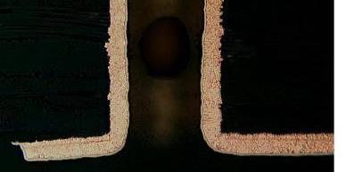
32 rates associated with raising the reflow peak temperature above 245 o C. Again, boards subjected to 6 passes at 245 o C performed significantly better compared to those conditioned for 3 profiles at 26 o C. Similar trends in improving fatigue life by reducing the number of reflow passes or by reducing the peak reflow temperatures, are again clearly indicated. Periodic Thermal Cycling Data SD 8:1 Vias 1 9 % Cumulative Failures Thermal Cycles Decreasing reflow passes Decreasing reflow temp. SDH8MS SDH6MS SDH3MS SDM6MS SDL6MS Figure 31: Comparison of cumulative periodic monitoring electrical test failures during thermal cycling for 8:1 vias in SD material with three conditioning profiles (23, 245 & 26 O C), and for 3, 6 and 8 Reflows A comparison of the cumulative failures for 1:1 vias thermally cycled after 6 reflows at 26 C in all four board materials, is provided in Figure 32. The two materials exhibiting the worst performance were SD and HD, the materials with the highest CTE above and below their glass transition temperatures. The HD material has the higher Tg, and therefore slightly improved performance over the SD material. Figures 33 to 36 present images of typical 1:1 vias after thermal cycling. In all sections, concertina-like collapsing of the vias was present, with fatigue cracks in all copper barrels. Failures were generally through the centre of the via barrel. However, with the HP and SP materials, the concertina-like collapsing was less heavy and the nickel outer plating on these vias was not ruptured, maintaining the electrical continuity of the via. If these boards had been finished without the nickel plate (as in the case of OSP or silver finish), these boards would have exhibited significantly more failures. 26


33 Periodic Thermal Cycling Data SD/SP/HD/HP 26 6 reflows 1:1 Vias % Cu m ul ati ve Fa ilu re s SD Low Tg, High CTE HD High Tg, Med/High CTE HP High Tg, Low CTE SP Med Tg, Med TCE Thermal Cycles SDH6T HPH6T SPH6T HDH6T Figure 32: Comparison of cumulative periodic electrical test failures during thermal cycling for 1:1 vias, for four material types (SD, SP, HD & HP), for 6 reflows and a peak reflow temperature of 26 o C 1mm 4μm Figure 33: Micro-sections of typical 1:1 via in SD material after 2 thermal cycles showing heavy concertina-like collapsing of vias, and failure of copper and nickel in the via wall 27


34 2μm 4μm 4μm Figure 34: Micro-sections of typical 1:1 via in HD material after 2 thermal cycles showing heavy concertina-like collapsing of vias, and failure of copper and nickel in the via wall 2μm 4μm 4μm Figure 35: Micro-sections of typical 1:1 via in SP material after 2 thermal cycles showing heavy concertina-like collapsing of vias, and failure of copper but intact nickel at the via wall 28


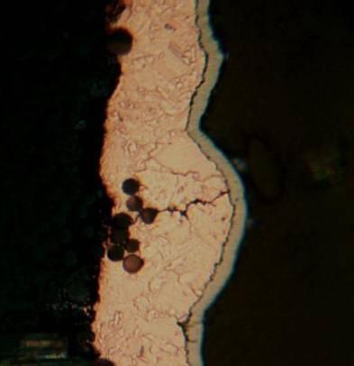
35 2μm 4μm 4μm Figure 36: Micro-sections of typical 1:1 via in HP material after 2 thermal cycles showing concertina-like collapsing of vias, and failure of copper but intact nickel in the via wall Figure 37 provides a comparison of the cumulative failures for 8:1 vias thermally cycled after 6 reflows at 26 C on all four board materials. Comparing these data with those of the 1:1 failures, there is little difference for the SD material. Its high CTE again produced increased stress on the vias and earlier failures. However, for these larger aspect vias, the HD material exhibited much improved fatigue life performance. As with the 1:1 results, there were few failures for the SP material. However, for the HP material, there were increased failures compared with the 1:1 via data. The probable cause for these premature failures is highlighted in Figure 38. The nickel layer, which was intact for the 1:1 HP vias in Figure 36, had been fractured for the equivalent 8:1 via shown on the right in Figure 38. It should be noted that compared to the thickness of the nickel of the SP material shown in the left of Figure 38, that for the HP material was significantly less, resulting in the earlier failure i.e fewer thermal cycling failures. The 1:1 vias did not contain the thinner nickel layer. Again, in the SP material, fracturing of the copper barrel was evident, but the nickel barrier was intact, maintaining the electrical continuity of the vias. 29

 and HP (right) showing differences in nickel thickness on 8:1")
36 Periodic Thermal Cycling Data SD/SP/HD/HP 26 6 reflows 8:1 Vias 1 9 SD Low Tg, High TCE 8 % Cumulative Failures HP High Tg, Low TCE SDH6MS HPH6MS SPH6MS HDH6MS 2 1 HD High Tg, Med TCE SP Med Tg, Med TCE Thermal Cycles Figure 37: Comparison of cumulative periodic electrical test failures during thermal cycling for 8:1 vias, for four material types (SD, SP, HD & HP), for 6 reflows and a peak reflow temperature of 26 O C 4μm Figure 38: Comparison of micro-sections for SP (left) and HP (right) showing differences in nickel thickness on 8:1 via walls 3
37 For 6:1 vias and micro-vias, the only significant failures occurred in the SD material (Figure 21 and 22). In both cases, more failures occurred with higher processing temperatures and with a greater number of reflow profiles. The annotated data for the 6:1 via data are shown in Figure 39. Indeed, for the micro-vias, significant failures only occurred for six and eight reflows at the 26 o C peak temperature profile. Periodic Thermal Cycling Data 6:1 Vias 1 % Cumulative Failures Decreasing number of profiles Decreasing reflow temp SDH8WS SDH6WS SDH3WS SDM6WS SDL6WS HPH8WS HPH6WS HPH3WS HPM6WS HPL6WS SPH6WS 1 HDH6WS Thermal Cycles Figure 39: Annotated cumulative periodic electrical test failures during thermal cycling for 6:1 vias, for four material types (SD, SP, HD & HP), three conditioning profiles (23, 245 & 26 O C) and for 3, 6 and 8 reflows 4.5 CONTINUITY MONITORING DATA For those samples continuously monitored, failures were restricted to the larger aspect ratio samples. There were no failures in the 6:1 vias for the SP, HD or HP materials for 6 reflows at 26 O C. Moreover, the SP material did not exhibit any failures for 8:1 vias. Continuous monitoring was not undertaken on micro-via samples.. The annotated data shown in Figures 23 to 27 exhibited similar trends to those of the periodically monitored data - decreasing via aspect ratio or decreasing peak reflow temperature, resulted in increased cycles to failure. The poorer performance of the SD material can again be attributed to its high CTE and low Tg. There were few differences in the trends in performance between samples having different aspect ratios for the SD material reflowed at 26 C peak reflow temperature. 31
38 Table 12 and again display the trends highlighted after periodic monitoring; the SD material performs poorer than the HD, SP and HP materials, the higher aspect ratio samples perform better, as do samples subjected to lower peak reflow temperatures. Table 12: Calculated N (1%) failure values Material Reflow O C Passes 1:1 8:1 6:1 SD SD * 45 SP HD HP A comparison between periodic monitoring data and continuity monitoring data for the same data sets, is presented in Figure 4. In the case of periodic monitoring, the failures clearly develop at a later stage even though the failure criterion (>1Ω) is less than that for the continuous monitoring (>3KΩ). The first failure with the periodic monitoring occurs at approximatley double the number of cycles observed in the continuous monitoring. The via failures intially develop as intermittent contacts (captured by the continuous monitoring), and are generally observed above 6 C on the positive ramp. When the vias have cooled to room temperature (where periodic monitoring is undertaken), the vias have contracted, and the small fatigue cracks have closed, thus reviving the continuity through the via. Periodic Thermal Cycling Data 8:1 Vias Probability Plot for SDL6MS-SDH6MS Weibull Distribution - LSXY Estimates Type 1 (Time) Censored at 3. 1 SDL6MS % Cumulative Failures Thermal Cycles SDH8MS SDH6MS SDH3MS SDM6MS SDL6MS HPH8MS HPH6MS HPH3MS HPM6MS HPL6MS SPH6MS HDH6MS Percent Time to Failure 1 HDH6MS HPH6MS SDH6MS Shape Scale r F/C / / / / Figure 4: Comparison of periodic monitoring data and continous monitoring data 32
39 5 CONCLUSIONS PCBs have been fabricated using four different base laminate materials commonly used by the electronic industry. These materials were both standard and high glass transition temperature (Tg) epoxy systems, with both dicy and phenolic curing agents. The assemblies were conditioned using reflow soldering profiles with peak soldering temperatures of 23, 245 and 26 o C, for up to 8 reflows. After conditioning, the assemblies were thermally cycled for up to 3 cycles and the electrical resistance of 1:1, 8:1, 6:1 and micro-vias was monitored. The fatigue failures generated by thermal cycling were dominated by barrel cracking. Micro-sectioning of failed vias showed heavy concertina-like collapsing of barrels, and fatigue cracks through the copper walls. In the vias where the stress during reflow was highest (i.e. materials with a high z-axis CTE, high aspect ratio vias, and/or higher number of reflow profiles), the nickel over-plate was also fractured causing via failure. In other cases, copper failures were still present but the nickel was intact. These thermal cycling failures generally occurred at the mid-point through the board, within the barrel. For the standard Tg dicy-cured material, the majority of via chains conditioned with a peak reflow temperature of 26 o C, had failed by 1 thermal cycles, irrespective of via aspect ratio. Lowering the peak reflow temperature to 245 o C extended the fatigue life to around 2 cycles. When the reflow temperatures were further lowered to SnPb processing levels (23 o C peak) then some SD via chains remained intact after 3 cycles. For the other materials, the majority of via chains survived 3 thermal cycles, even for 1:1 aspect ratio vias. The exception was the 1:1 vias in the HD (high Tg dicy-cured) material. Although this material had a high Tg, its z-axis CTE was higher than that of the SP (standard Tg phenolic-cured) or HP (high Tg phenolic-cured) materials, and this resulted in earlier failures. Significant failures were also noted for the HP material for 8:1 vias conditioned with a 26 o C peak reflow temperature. Microsections of failed joints highlighted thinner nickel plating on these vias, which may have contributed to their earlier failure. Comparison between the batches of PCBs allowed the following conclusions: Higher processing temperatures result in earlier failures Increasing peak reflow temperature above 245 o C may significantly increase the failure rate, and may result in a step function decrease in lead-free reliability Increasing the number of profiles results in earlier failures Higher aspect ratio vias fail earlier than lower aspect ratio vias Materials with high z-axis CTE performed worst during thermal cycling Increasing Tg improves via reliability, but lower Tg, lower CTE materials have been shown to out perform higher Tg, higher CTE materials Some samples were monitored for electrical resistance both periodically (every 5 cycles) or continuously. In the case of periodic monitoring, the failures clearly developed at a later stage even though the failure criterion (>1Ω) was greater than 33
40 that for the continuous monitoring (>3KΩ). In the case of continuous monitoring typically failures initiate at 5% to 75% of the fatigue life for the first failures for periodic monitoring. The failures first develop as intermittent contacts which are measurable as short duration open circuits, generally on the positive ramp, approximately at 8 C. By the time the vias have cooled to room temperature (where the periodic monitoring measurements are undertaken), the vias have contracted, closing the small fatigue cracks and reviving the continuity through the via. The first phase of this work has shown that a test method for testing these materials is achievable. The test is sensitive for measuring the effect of the higher temperatures associated with lead-free soldering on the reliability of electronic substrates. The results from these tests will improve industry confidence in the reliability of PCB substrates during and after the change to lead-free processes. 6 ACKNOWLEDGEMENTS The work was carried out as part of a project in the Materials Processing Metrology Programme of the UK Department for Innovation, Universities and Skills. We gratefully acknowledge the support and co-operation of the following companies without whose help this project would not have been possible. BAE (INSYTE) Circatex Limited Dolby Laboratories Inc. (UK) Fujitsu Telecommunications Europe Ltd Goodrich Engine Controls Graphic Plc Isola Werke UK Limited MBDA (UK) Ltd NEC Panda Europe Polar Instruments UK Ltd Polyclad Europe PWB Interconnect Solutions Inc Rockwell Collins Rolls Royce Marine Substrate Systems Limited (SSL) Thales Missile Electronics Ltd TRW Automotive Technical Centre, Solihull In addition, we would like to acknowledge the material support provided by the following individuals and companies, which made the project possible. Gerald Rutter and Peter Franklin, BTU Europe Paul Comer and Kerry Hewlett, Graphic Plc Sam Gnaniah, Roger Morrell, Madeleine Peck and Ling Zou, National Physical Laboratory Bill Birch and Jason Furlong, PWB Interconnect Solutions Inc Dave Hillman and Bob Miller, Rockwell Collins for some of the sectioning Mark Newton and Mick White, Thales Missile Electronics Ltd 34
41 7 REFERENCES (1) PWB Corp. IST report, private communication (2) Glass transition temperature of organic films - DMA Method IPC-TM (3) Thermal analysis techniques for composites and adhesives D R Mulligan, S J P Gnaniah, G D Sims, NPL Good Practice Guide GPG (4) Standard test method for rapid thermal degradation of solid electrical insulating materials by thermogravimetric method (TGA). D
Lead Free Assembly: A Practical Tool For Laminate Materials Selection
 Lead Free Assembly: A Practical Tool For Laminate Materials Selection Erik J. Bergum David Humby Isola Abstract: The impending European RoHS legislation, restricting the use of lead containing solders,
BASE MATERIALS Through Assembly
 Thermal Analysis of BASE MATERIALS Through Assembly Can current analytical techniques predict and characterize differences in laminate performance prior to exposure to thermal excursions during assembly?
Low CTE / High Tg FR-4 with High Heat Resistance
 Low CTE / High Tg FR-4 with High Heat Resistance Laminate: EM-827 Prepreg: EM-827B 1 Features Tg(DSC) > 170 Z direction CTE < 3.0% (50~260 ) High thermal degradation temperature: Td > 340 Excellent thermal
NPL Report MATC(A)91 An Assessment of the Suitability of Current PCB Laminates to Withstand Lead-free Reflow Profiles
91 An Assessment of the Suitability of Current PCB Laminates to Withstand Lead-free Reflow Profiles") An Assessment of the Suitability of Current PCB Laminates to Withstand Lead-free Reflow Profiles Martin Wickham, Ling Zou & Christopher Hunt April 2002 Crown copyright 2002 Reproduced by permission of
An Assessment of the Suitability of Current PCB Laminates to Withstand Lead-free Reflow Profiles Martin Wickham, Ling Zou & Christopher Hunt April 2002 Crown copyright 2002 Reproduced by permission of
Component Palladium Lead Finish - Specification Approved by Executive Board 1997-xx-xx August 22 Version
 Component Palladium Lead Finish - Specification Approved by Executive Board 1997-xx-xx August 22 Version Appendices 1. User Commitment Form 2. Supplier Compliance Form Table of contents 1. Background 2.
PCB Production Process HOW TO PRODUCE A PRINTED CIRCUIT BOARD
 NCAB Group Seminars PCB Production Process HOW TO PRODUCE A PRINTED CIRCUIT BOARD NCAB GROUP PCB Production Process Introduction to Multilayer PCBs 2 Introduction to multilayer PCB s What is a multilayer
Characterizing the Lead-Free Impact on PCB Pad Craters
 Characterizing the Lead-Free Impact on PCB Pad Craters Brian Roggeman and Wayne Jones Advanced Process Lab Universal Instruments Corp. Binghamton, NY 13902 Abstract Pad cratering in Printed Circuit Boards
Composition/wt% Bal SA2 (SABI) Bal SA3 (SABI + Cu) Bal
 Bal SA3 (SABI + Cu) Bal") Improving Thermal Cycle and Mechanical Drop Impact Resistance of a Lead-free Tin-Silver-Bismuth-Indium Solder Alloy with Minor Doping of Copper Additive Takehiro Wada 1, Seiji Tsuchiya 1, Shantanu Joshi
Improving Thermal Cycle and Mechanical Drop Impact Resistance of a Lead-free Tin-Silver-Bismuth-Indium Solder Alloy with Minor Doping of Copper Additive Takehiro Wada 1, Seiji Tsuchiya 1, Shantanu Joshi
c/bach, 2-B Pol. Ind Foinvasa Montcada i Reixac (Barcelona) SPAIN Tel FAX
 SPAIN Tel FAX") 1- What is 2- How does it work? 3- How do we make it? 4- Applications 5- Processing? WHAT IS? Thick aluminium based substrate, cladded in ED copper foil. Designed for an effective thermal dissipation and
1- What is 2- How does it work? 3- How do we make it? 4- Applications 5- Processing? WHAT IS? Thick aluminium based substrate, cladded in ED copper foil. Designed for an effective thermal dissipation and
Test Methods for Evaluating the Reliability of PCB Finishes using Lead-Free Alloys - A Guide
 NPL Report MATC(A) 107 Test Methods for Evaluating the Reliability of PCB Finishes using Lead-Free Alloys - A Guide Milos Dusek & Christopher Hunt April 2002 Test Methods for Evaluating the Reliability
GRAPHIC MANUFACTURING CAPABILITY Q217-18
 All features are design dependent and may not be achievable in combination Reduced Yield / Special values up ( or down ) to the standard limit are design and application dependent Standard features only
SOLDER JOINT RELIABILITY TEST SUMMARY
 Project Number: SJR Tracking Code: TC0623-SEAF-SJR-1059 Requested by: Jeremy Wooldridge Date: 05/20/2008 Product Rev: D (SEAF), C (SEAM) Part #: SEAF-50-5.0-S-10-2-A/ SEAM-50-2.0-S-10-2-A SEAF-50-6.5-S-10-1-A/
Lead-Free Solder Bump Technologies for Flip-Chip Packaging Applications
 Lead-Free Solder Bump Technologies for Flip-Chip Packaging Applications Zaheed S. Karim 1 and Jim Martin 2 1 Advanced Interconnect Technology Ltd. 1901 Sunley Centre, 9 Wing Yin Street, Tsuen Wan, Hong
WF6317. A superactive low-volatile/high heat-resistant water-soluble flux for ball soldering
 WF637 A superactive low-volatile/high heat-resistant water-soluble flux for ball soldering Low viscosity and high tacking power stabilize ball holding force and ensures excellent solder wettability Easy
System Level Effects on Solder Joint Reliability
 System Level Effects on Solder Joint Reliability Maxim Serebreni 2004 2010 Outline Thermo-mechanical Fatigue of solder interconnects Shear and tensile effects on Solder Fatigue Effect of Glass Style on
Ultralow Residue Semiconductor Grade Fluxes for Copper Pillar Flip-Chip
 Ultralow Residue Semiconductor Grade Fluxes for Copper Pillar Flip-Chip SzePei Lim (Presenter), Jason Chou, Maria Durham, and Dr. Andy Mackie Indium Corporation 1 Outline of Presentation Roadmaps and challenges
New Pb-Free Solder Alloy for Demanding Applications. Presented by Karl Seelig, VP Technology, AIM
 New Pb-Free Solder Alloy for Demanding Applications Presented by Karl Seelig, VP Technology, AIM Why REL? The evolution and expansion of electronics into more harsh operating environments performing more
Reliability of Interconnects in LED Lighting Assemblies Utilizing Metal Clad Printed Circuit Boards Stefano Sciolè BDM I.M.S.
 Reliability of Interconnects in LED Lighting Assemblies Utilizing Metal Clad Printed Circuit Boards Stefano Sciolè BDM I.M.S. Henkel Electronic Materials Agenda 1. Introduction 2. Motivation 3. Interconnect
Simulation of Embedded Components in PCB Environment and Verification of Board Reliability
 Simulation of Embedded Components in PCB Environment and Verification of Board Reliability J. Stahr, M. Morianz AT&S Leoben, Austria M. Brizoux, A. Grivon, W. Maia Thales Global Services Meudon-la-Forêt,
LEAD FREE ALLOY DEVELOPMENT
 LEAD FREE ALLOY DEVELOPMENT Karl F. Seelig, VP of Technology AIM Cranston, RI. USA. kseelig@aimsolder.com Abstract. When lead-free solders were first introduced to the electronics industry in the early
Validated Test Method to Characterize and Quantify Pad Cratering Under Bga Pads on Printed Circuit Boards
 Validated Test Method to Characterize and Quantify Pad Cratering Under Bga Pads on Printed Circuit Boards Mudasir Ahmad, Jennifer Burlingame, Cherif Guirguis Technology and Quality Group Cisco Systems,
ThunderClad 2. TU-883 HF Very Low Loss Material. Laminates & Prepregs Mass Lamination Service Insulated Metal Substrate Materials
 ThunderClad 2 TU-883 HF Very Low Loss Material Laminates & Prepregs Mass Lamination Service Insulated Metal Substrate Materials TUC Product Roadmap 2 ULVP VLP HCF Ultra Low Void Prepreg Very Low Profile
1/2W, 0805 Low Resistance Chip Resistor (Lead / Halogen free)
") 1. Scope 1/2W, 0805 (Lead / Halogen free) This specification applies to 1.2mm x 2.0mm size 1/2W, fixed metal film chip resistors rectangular type for use in electronic equipment. 2. Type Designation RL
1. Scope 1/2W, 0805 (Lead / Halogen free) This specification applies to 1.2mm x 2.0mm size 1/2W, fixed metal film chip resistors rectangular type for use in electronic equipment. 2. Type Designation RL
Gage Series Stress Analysis Gages
 GAGE SERIES All Micro-Measurements strain gages incorporate precision foil grids mounted on organic backing materials. The strain-sensing alloys and backing materials cannot be arbitrarily combined in
UL PCB Recognition what is it & why do you need to know about it
 UL PCB Recognition what is it & why do you need to know about it Presented by Emma Hudson NCAB Customer Event March 2015 UL and the UL logo are trademarks of UL LLC 2015 Agenda What is UL and what are
TECHNICAL DATA SHEET 1 P a g e Revised January 9, 2014
 1 P age Revised January 9, 2014 TAIYO PSR-4000 CC01SE (UL Name: PSR-4000JV / CA-40JV) LIQUID PHOTOIMAGEABLE CURTAIN COAT SOLDER MASK Curtain Coat Application Aqueous Developing Solder Mask RoHS Compliant
Reflow Profiling: Time a bove Liquidus
 Reflow Profiling: Time a bove Liquidus AIM/David Suraski Despite much research and discussion on the subject of reflow profiling, many questions and a good deal of confusion still exist. What is clear
How to select PCB materials for highfrequency
 How to select PCB materials for highfrequency apps Find out how to simplify that choice when striving for the best tradeoff between ease of fabrication and best electrical performance. By John Coonrod
contaminated, or if the location of the assembly house is well above sea level.
 VAPOR PHASE REFLOW S EFFECT ON SOLDER PASTE RESIDUE SURFACE INSULATION RESISTANCE Karen Tellefsen. Mitch Holtzer, Corne Hoppenbrouwers Alpha Assembly Solutions South Plainfield, NJ, USA Roald Gontrum SmartTech
ROHS Reliability Impact
 ROHS Reliability Impact A Reality Check!!!! Presented by Larry Akre May 17, 2007 LAkre 2007 1 ROHS Reliability Impact RoHS Directive 2002/95/EC WEEE Directive 2002/96/EC Failure Mechanisms Tin Whiskers
Optimizing the Insulated Metal Substrate Application with Proper Material Selection and Circuit Fabrication
 Abstract Optimizing the Insulated Metal Substrate Application with Proper Material Selection and Circuit Fabrication Dave Sommervold, Chris Parker, Steve Taylor, Garry Wexler. The Bergquist Company Prescott,
Environmental Friendly PWB & Packaging Materials
 Environmental Friendly PWB & Packaging Materials May 7. 2009 Electronic Materials Business Unit Agenda 2 1. Brief Introduction of Panasonic Electric Works (PEW) 1) Corporate and EMBU (Electronic Materials
Becoming Lead Free. Automotive Electronics. Antonio Aires Soldering Technical Specialist Visteon Corporation - Palmela Plant
 Automotive Electronics Becoming Lead Free Antonio Aires Soldering Technical Specialist Visteon Corporation - Palmela Plant 1 Agenda 1. Leadfree Electronics Drivers 2. Requirements 3. Areas of Impact 4.
High Frequency Circuit Materials Attributes John Coonrod, Rogers Corporation
 High Frequency Circuit Materials Attributes John Coonrod, Rogers Corporation Specialty high frequency circuit materials have been used in the PCB industry for decades and for many different reasons. There
DEVELOPMENT OF LEAD-FREE ALLOYS WITH ULTRA-HIGH THERMO- MECHANICAL RELIABILITY
 As originally published in the SMTA Proceedings. DEVELOPMENT OF LEAD-FREE ALLOYS WITH ULTRA-HIGH THERMO- MECHANICAL RELIABILITY Pritha Choudhury, Ph.D., Morgana Ribas, Ph.D., Ranjit Pandher, Ph.D., Anil
A New Approach for Early Detection of PCB Pad Cratering Failures
 A New Approach for Early Detection of PCB Pad Cratering Failures Anurag Bansal, Gnyaneshwar Ramakrishna and Kuo-Chuan Liu Cisco Systems, Inc., San Jose, CA anurbans@cisco.com Abstract Pad cratering refers
Newsletter. Test Services & Failure Analysis Laboratory. April The Reality of Flip-Chip Solder Bump Electromigration Failure INSIDE THIS ISSUE
 Test Services & Failure Analysis Laboratory April 2008 Newsletter INSIDE THIS ISSUE Features Solder Bump Electromigration Failure Solder Joint Failure Criteria External Inspection of PCBs Hollow Fibers
Highly Accelerated Thermal Shock Reliability Testing
 Highly Accelerated Thermal Shock Reliability Testing by Bob E. Neves Microtek Laboratories, Inc. Anaheim CA and Rick B. Snyder Delphi Delco Electronics Systems, Inc. Kokomo IN and Timothy A. Estes Conductor
Process & Capability Manual (Vol )
") Process & Capability Manual (Vol. 12-2015) Seite 1 von 13 1 CHAPTER OVERVIEW 1 CHAPTER OVERVIEW... 2 2 MICROCIRTEC A SHORT PROFILE... 3 2.1 WHO WE ARE... 3 2.2 OBJECTIVES & MARKETS... 3 2.3 DECLARATION
Process & Capability Manual (Vol. 12-2015) Seite 1 von 13 1 CHAPTER OVERVIEW 1 CHAPTER OVERVIEW... 2 2 MICROCIRTEC A SHORT PROFILE... 3 2.1 WHO WE ARE... 3 2.2 OBJECTIVES & MARKETS... 3 2.3 DECLARATION
RoHS Compliance Document
 D2-Pak RoHS Compliance Document Contents: 1. 2. Solder Reflow 3. Tin Whisker Report D2-pak (3 or 5 Lead) BOM 1 90598-46-2 0.05808 11% 3.8% Lead Frame Copper 0.94840 Die Attach Soft Solder 0.01200 Cu 7440-50-8
Eliminating Wave Soldering with Low Melting Point Solder Paste ABSTRACT Process Cost Reduction INTRODUCTION
 Eliminating Wave Soldering with Low Melting Point Solder Paste Mitch Holtzer and Tuck Weng Mok Alpha, an Alent plc Company 109 Corporate Blvd., South Plainfield, NJ 07080 USA Email: mholtzer@alent.com;
Welcome to the Real World of Lead Free Soldering
 Welcome to the Real World of Lead Free Soldering Metallic Resources, Inc. Howard Stevens Nimal Liyanage,, Ph.D Objective: to Provide Education Regarding the Effects of Various Lead Free Soldering Alloys
Critical Use Conditions and their Effect on the Reliability of Soldered Interconnects in Under the Hood Application
 1 Fraunhofer ISIT, Itzehoe Critical Use Conditions and their Effect on the Reliability of Soldered Interconnects in Under the Hood Application Dr. T. Ahrens and Mr. F. W. Wulff, CEM GmbH, Mr. S. Wiese,
Offshore Wind Turbines Power Electronics Design and Reliability Research
 Offshore Wind Turbines Power Electronics Design and Reliability Research F. P. McCluskey CALCE/Dept. Of Mechanical Engineering University of Maryland, College Park, MD (301) 405-0279 mcclupa@umd.edu 1
FLEXIBLE & RIGID-FLEX CIRCUITS TECHNICAL ENGINEERING GUIDE. Delivering Quality Since 1952.
 FLEXIBLE & RIGID-FLEX CIRCUITS TECHNICAL ENGINEERING GUIDE Delivering Quality Since 1952. DELIVERING QUALITY SINCE 1952. Epec Engineered Technologies designs and manufactures customized, built-to-print,
Atmosphere Effect on Soldering of Flip Chip Assemblies. C. C. Dong Air Products and Chemicals, Inc. U.S.A.
 Atmosphere Effect on Soldering of Flip Chip Assemblies C. C. Dong Air Products and Chemicals, Inc. U.S.A. Atmosphere Effect on Soldering of Flip Chip Assemblies Abstract An experimental study was conducted
Qualification and Performance Specification for Flexible Printed Boards
 Qualification and Performance Specification for Flexible Printed Boards Developed by the Flexible Circuits Performance Specifications Subcommittee (D-12) of the Flexible Circuits Committee (D-10) of IPC
ALTERNATIVES TO SOLDER IN INTERCONNECT, PACKAGING, AND ASSEMBLY
 ALTERNATIVES TO SOLDER IN INTERCONNECT, PACKAGING, AND ASSEMBLY Herbert J. Neuhaus, Ph.D., and Charles E. Bauer, Ph.D. TechLead Corporation Portland, OR, USA herb.neuhaus@techleadcorp.com ABSTRACT Solder
INFLUENCE OF ELECTRICALLY CONDUCTIVE ADHESIVE AMOUNT ON SHEAR STRENGTH OF GLUED JOINTS ON FLEXIBLE SUBSTRATES
 INFLUENCE OF ELECTRICALLY CONDUCTIVE ADHESIVE AMOUNT ON SHEAR STRENGTH OF GLUED JOINTS ON FLEXIBLE SUBSTRATES ABSTRACT: Martin Hirman and František Steiner Department of Technologies and Measurement Faculty
ROLINX Laminated Busbar. Design Rules Version 01 (12/2015)
") ROLINX Laminated Busbar Design Rules Version 01 (12/2015) Content 1. Introduction... 03 7. Features... 13 2. Configuration...03 8. Thermal parameters... 14 3. Products... 04 9. General parameters... 14
ROLINX Laminated Busbar Design Rules Version 01 (12/2015) Content 1. Introduction... 03 7. Features... 13 2. Configuration...03 8. Thermal parameters... 14 3. Products... 04 9. General parameters... 14
The hand soldering process can therefore be defined by the following steps ;
 Hand Soldering with Lead Free Alloys Introduction As companies start to implement lead free soldering processes, hand soldering and associated techniques have been identified as key functions in the manufacturing
Recent Advances in Die Attach Film
 Recent Advances in Die Attach Film Frederick Lo, Maurice Leblon, Richard Amigh, and Kevin Chung. AI Technology, Inc. 70 Washington Road, Princeton Junction, NJ 08550 www.aitechnology.com Abstract: The
Conductive Anodic Filament Growth Failure
 Presented at IPC Printed Circuits Expo www.ipcprintedcircuitexpo.org Conductive Anodic Filament Growth Failure Tarun Amla Isola Abstract With increasing focus on reliability and miniaturized designs, Conductive
3D-WLCSP Package Technology: Processing and Reliability Characterization
 3D-WLCSP Package Technology: Processing and Reliability Characterization, Paul N. Houston, Brian Lewis, Fei Xie, Ph.D., Zhaozhi Li, Ph.D.* ENGENT Inc. * Auburn University ENGENT, Inc. 2012 1 Outline Packaging
IMPACT OF MICROVIA-IN-PAD DESIGN ON VOID FORMATION
 IMPACT OF MICROVIA-IN-PAD DESIGN ON VOID FORMATION Frank Grano, Felix Bruno Huntsville, AL Dana Korf, Eamon O Keeffe San Jose, CA Cheryl Kelley Salem, NH Joint Paper by Sanmina-SCI Corporation EMS, GTS
ESPANEX L Series. Technical data sheet Nishigotanda Shinagawa Tokyo, , Japan TEL FAX
 ESPANEX L Series Technical data sheet This sheet will be changed without any information in advance. The data on this sheet are solely for your reference and are not to be constructed as constituting a
IPC-TM-650 TEST METHODS MANUAL
 3000 Lakeside Drive, Suite 309S Bannockburn, IL 60015-1249 TEST METHODS MNUL Number Conductive nodic Filament (CF) Resistance Test: X-Y xis Originating Task Group Electrochemical Migration Task Group (5-32e)
Cal-Chip Electronics, Incorporated Thick Film Chip Resistors - RM Series
 Thick Film Chip Resistors - RM Series Fixed Chip Resistors manufactured for more compact electronic components and automatic mounting system. These Chip Resistors have electrical stability and mechanical
14. Designing with FineLine BGA Packages
 14. Designing with FineLine BGA Packages S51014-1.0 Chapter 14, Designing with FineLine BGA Packages, replaces AN 114: Designing with FineLine BGA Packages. Introduction As programmable logic devices (PLDs)
High Tg Bromine-free Laminates for PWB Applications
 Presented at IPC Printed Circuits EXPO www.ipcprintedcircuitexpo.org High Tg Bromine-free Laminates for PWB Applications Marty Choate Isola Abstract The development of halogen free materials has been a
Flexible PCB Plating Through Hole Considerations, Experiences and Solutions
 Presented in the ECWC 10 Conference at IPC Printed Circuits Expo, SMEMA Council APEX and Designers Summit 05 Flexible PCB Plating Through Hole Considerations, Experiences and Solutions Neil Patton Atotech
Nano- And Micro-Filled Conducting Adhesives For Z-axis Interconnects
 Nano- And Micro-Filled Conducting Adhesives For Z-axis Interconnects We take a look at micro-filled epoxy-based conducting adhesives modified with nanoparticles for z- axis interconnections, especially
A STUDY OF THE ENEPIG IMC FOR EUTECTIC AND LF SOLDERS
 A STUDY OF THE ENEPIG IMC FOR EUTECTIC AND LF SOLDERS G.Milad, D.Gudeczauskas, G.Obrien, A.Gruenwald Uyemura International Corporation Southington, CT ABSTRACT: The solder joint formed on an ENEPIG surface
High Stability Resistor Chips (< 0.25 % at Pn at 70 C during 1000 h) Thick Film Technology
 Thick Film Technology") High Stability Resistor Chips (< 0.25 % at Pn at 70 C during 0 h) Thick Film Technology thick film resistor chips are specially designed to meet very stringent specifications in terms of reliability, stability
High Stability Resistor Chips (< 0.25 % at Pn at 70 C during 0 h) Thick Film Technology thick film resistor chips are specially designed to meet very stringent specifications in terms of reliability, stability
Lead-Free Connectors - An Overview
 Lead-Free Connectors - An Overview Pete Elmgren Molex Inc. 15 August 2003 Introduction For more than 50 years, lead-bearing solders have been used almost exclusively throughout the electronics industry
Effects of Solder Reflow Conditions on the Assembly of Electronics Packaging and Printed Circuit Boards
 Effects of Solder Reflow Conditions on the Assembly of Electronics Packaging and Printed Circuit Boards Gregory K. Arslanian, Minfa Lin, Amy Wressell, Tom Mebrahtu, Victor Wang Air Products and Chemicals
PCB Technologies for LED Applications Application note
 PCB Technologies for LED Applications Application note Abstract This application note provides a general survey of the various available Printed Circuit Board (PCB) technologies for use in LED applications.
Basic PCB Level Assembly Process Methodology for 3D Package-on-Package
 Basic PCB Level Assembly Process Methodology for 3D Package-on-Package Vern Solberg STC-Madison Madison, Wisconsin USA Abstract The motivation for developing higher density IC packaging continues to be
Flex and Rigid-Flex Printed Circuit Design
 Flex and Rigid-Flex Printed Circuit Design Old Content - visit altium.com/documentation Modified by on 29-Nov-2016 Related Videos Bending Lines Enhanced Layer Stack Management Layer Stack Regions A rigid-flex
1/2W, 0612 Low Resistance Chip Resistor (Lead / Halogen Free)
") 1/2W, 0612 (Lead / Halogen Free) 1. Scope This specification applies to 1.6mm x 3.2mm size 1/2W, fixed metal film chip resistors rectangular type for use in electronic equipment. 2. Type Designation RL1632W
1/2W, 0612 (Lead / Halogen Free) 1. Scope This specification applies to 1.6mm x 3.2mm size 1/2W, fixed metal film chip resistors rectangular type for use in electronic equipment. 2. Type Designation RL1632W
An Innovative High Throughput Thermal Compression Bonding Process
 An Innovative High Throughput Thermal Compression Bonding Process Li Ming 2 September 2015 Outline Introduction Throughput improved TCB Process Liquid Phase Contact (LPC) bonding Flux-LPC-TCB under inert
FYS4260/FYS9260: Microsystems and Electronics Packaging and Interconnect Printed Circuit Boards
 FYS4260/FYS9260: Microsystems and Electronics Packaging and Interconnect Printed Circuit Boards Interior detail from an Apple iphone 5 printed circuit board Learning objectives Understand how printed wiring/circuit
Impact of Intermetallic Growth on the Mechanical Strength of Pb-Free BGA Assemblies
 Impact of Intermetallic Growth on the Mechanical Strength of Pb-Free BGA Assemblies Patrick Roubaud, Grace Ng, Greg Henshall Hewlett Packard Ronald Bulwith, Robert Herber - Alpha Metals Swaminath Prasad,
DuPont Kapton FPC POLYIMIDE FILM
 DuPont FPC POLYIMIDE FILM Technical Data Sheet DuPont FPC polyimide film is treated on both sides and has the same excellent balance of physical, chemical and electrical properties over a wide temperature
Thermo-Mechanical FEM Analysis of Lead Free and Lead Containing Solder for Flip Chip Applications
 Thermo-Mechanical FEM Analysis of Lead Free and Lead Containing Solder for Flip Chip Applications M. Gonzalez 1, B. Vandevelde 1, Jan Vanfleteren 2 and D. Manessis 3 1 IMEC, Kapeldreef 75, 3001, Leuven,
Reference Only. Spec. No. JENF243D-0006K-01 P 1/ 8
 Spec. No. JENF243D-0006K-01 P 1/ 8 Chip EMIFIL LC Combined Monolithic NFL21SP X1C Reference Specification 1. Scope This reference specification applies to Chip EMIFIL LC Combined Monolithic Type NFL21S
Reference Only. Spec. No. JENF243E-0003Q-01 P 1 / 8. Chip EMIFIL LC Combined Type for Large Current NFE61PT 1H9 Reference Specification
 Spec. No. JENF243E-0003Q-01 P 1 / 8 Chip EMIFIL LC Combined Type for Large Current NFE61PT 1H9 Reference Specification 1. Scope This reference specification applies to Chip EMIFIL LC Combined Type for
Failure Modes in Wire bonded and Flip Chip Packages
 Failure Modes in Wire bonded and Flip Chip Packages Mumtaz Y. Bora Peregrine Semiconductor San Diego, Ca. 92121 mbora@psemi.com Abstract The growth of portable and wireless products is driving the miniaturization
Reliability Screening of Lower Melting Point Pb-Free Alloys Containing Bi
 Reliability Screening of Lower Melting Point Pb-Free Alloys Containing Bi Joseph M. Juarez, Jr., Michael Robinson, Joel Heebink Honeywell AZ, US mike.robinson6@honeywell.com joseph.juarez@honeywell.com
Visit
 UV Inspection and Thickness Measurement of Conformal Coatings Vimal Gopee, NPL Vimal.gopee@npl.co.uk Electronic & Magnetic Materials Group 1 Your Delegate Webinar Control Panel Open and close your panel
curamik CERAMIC SUBSTRATES AMB technology Design Rules Version #04 (09/2015)
") curamik CERAMIC SUBSTRATES AMB technology Design Rules Version #04 (09/2015) Content 1. Geometric properties 1.01. Available ceramic types / thicknesses... 03 1.02. thicknesses (standard)... 03 3. Quality
curamik CERAMIC SUBSTRATES AMB technology Design Rules Version #04 (09/2015) Content 1. Geometric properties 1.01. Available ceramic types / thicknesses... 03 1.02. thicknesses (standard)... 03 3. Quality
Black 1:1 Epoxy, Encapsulating & Potting Compound
 Technical Data Sheet Black 1:1 Epoxy, Encapsulating & Potting Compound Description 832HD potting and encapsulating compound is a general purpose, hard, black, two-part epoxy that offers extreme environmental,
Green Product. 2 nd level reliability of tin plated components. Dr. Marc Dittes CAT AIT PGP
 Green Product 2 nd level reliability of tin plated components Infineon Outline Experimental parameters Testboard, paste, components, T-cycling, Shear test Reflow profile SnPbAg Reflow profile SnAgCu Reliability
Novel Materials and Activities for Next Generation Package. Hitachi Chemical., Co.Ltd. Packaging Solution Center Hiroaki Miyajima
 Novel Materials and Activities for Next Generation Package Hitachi Chemical., Co.Ltd. Packaging Solution Center Hiroaki Miyajima 1. Activities of Packaging Solution Center 2. Novel Materials for Next Gen.
Chips Face-up Panelization Approach For Fan-out Packaging
 Chips Face-up Panelization Approach For Fan-out Packaging Oct. 15, 2015 B. Rogers, D. Sanchez, C. Bishop, C. Sandstrom, C. Scanlan, TOlson T. REV A Background on FOWLP Fan-Out Wafer Level Packaging o Chips
High Performance Alloys. Characteristics
 Alloy Designation EN DIN CEN/TS 13388 UNS High Performance Alloys Chemical Composition Weight percentage We have developed a wide range of high performance alloys with excellent properties regarding conductivity,
Discrete Capacitor & Resistor Issues. Anthony Primavera Boston Scientific CRM 11/13/06
 Discrete Capacitor & Resistor Issues Anthony Primavera Boston Scientific CRM 11/13/06 Goal: Drive the Industry towards common test methods and best practices in manufacturing to reduce and or eliminate
COMPONENT LEVEL RELIABILITY FOR HIGH TEMPERATURE POWER COMPUTING WITH SAC305 AND ALTERNATIVE HIGH RELIABILITY SOLDERS
 As originally published in the SMTA Proceedings. COMPONENT LEVEL RELIABILITY FOR HIGH TEMPERATURE POWER COMPUTING WITH SAC305 AND ALTERNATIVE HIGH RELIABILITY SOLDERS Thomas Sanders, Sivasubramanian Thirugnanasambandam
White Paper Quality and Reliability Challenges for Package on Package. By Craig Hillman and Randy Kong
 White Paper Quality and Reliability Challenges for Package on Package By Craig Hillman and Randy Kong Background Semiconductor technology advances have been fulfilling Moore s law for many decades. However,
SHAPE MEMORY EFFECT OF A THERMOSET POLYMER AND ITS FIBER REINFORCED COMPOSITES
 18 TH INTERNATIONAL CONFERENCE ON COMPOSITE MATERIALS SHAPE MEMORY EFFECT OF A THERMOSET POLYMER AND ITS FIBER REINFORCED COMPOSITES C. Ayranci 1, F. Ko 1*, T. Howie 2, M.Taya 2 1 Department Materials
STANDARD FERRITIC STAINLESS STEELS
 T e c h n i c a l B r o c h u r e STANDARD FERRITIC STAINLESS STEELS Unity AISI UNS EN U-40910 409 S40910 1.4512 U-430 430 S43000 1.4016 U-430DDQ 430 S43000 1.4016 U-439 439 S43035 1.4510 - S43940 U-1.4509
INTERFLUX ELECTRONICS NV
 Reflow soldering temperature profiling Min : 30sec Max : 120sec Max : +4 C/sec Max : 250 C Min : 230 C Min: +0,5 C/sec Min : +1 C/sec Max : +3 C/sec Max : +1 C/sec Max : -6 C/sec Min : -2 C/sec Min : +1
Low Profile 0.5mm Pitch Connectors For FPC
 Low Profile 0.5mm Pitch Connectors For FPC FH17 Series FH17 (on-board type) flip-lock mechanism Features 1. Low profile 0.5mm pitch FPC connectors As products become lighter/thinner/shorter/smaller, requests
Hitachi Anisotropic Conductive Film ANISOLM AC-8955YW. Issued 2007/03/30
 Hitachi Chemical Data Sheet Hitachi Anisotropic Conductive Film ANISOLM AC-8955YW Issued 27/3/3 1. Standard specification, bonding condition, storage condition and characteristic...1 2. Precautions in
Material Selection and Parameter Optimization for Reliable TMV Pop Assembly
 Selection and Parameter Optimization for Reliable TMV Pop Assembly Brian Roggeman, David Vicari Universal Instruments Corp. Binghamton, NY, USA Roggeman@uic.com Martin Anselm, Ph.D. - S09_02.doc Lee Smith,
DATA SHEET Metal Element Current Sensing Chip Resistor CLS Series
 DATA SHEET Metal Element Current Sensing Chip Resistor 0.5% TO 5%, TCR ±25 TO ±450 SIZE: 1206/2010/2512/2725/2728/4527/4527S RoHs Compliant 14 October, 2016 V.4 DS-ENG-007 23 Page: 2 of 1. SCOPE 1.1 This
Effects of SAC Alloy Copper Dissolution Rates on PTH Processes: Cost and performance justify use of certain alternatives to SAC305/405
 Effects of SAC Alloy Copper Dissolution Rates on PTH Processes: Cost and performance justify use of certain alternatives to SAC305/405 1 Craig Hamilton, Polina Snugovsky (Celestica) & Matthew Kelly (IBM)
ROUND ROBIN TESTING OF CREEP CORROSION DEPENDENCE ON RELATIVE HUMIDITY
 ROUND ROBIN TESTING OF CREEP CORROSION DEPENDENCE ON RELATIVE HUMIDITY Prabjit Singh and Larry Palmer Corporation, Poughkeepsie, New York, USA pjsingh@us.ibm.com Haley Fu International Electronics Manufacturing