High-end solutions for high-tech industries. Dr. Sebastian Gatz, Klaus Ruhmer
|
|
|
- Abraham Walton
- 6 years ago
- Views:
Transcription


1 High-end solutions for high-tech industries Dr. Sebastian Gatz, Klaus Ruhmer

2 Focus on technology Meyer Burger is a leading global technology company specializing in innovative systems and processes based on semiconductor technologies. The company s focus is on photovoltaics while its competencies and technologies also cover important areas of the semiconductor and the optoelectronic industries as well as other selected high-end markets based on semiconductor materials.


3 Global infrastructure at a glance The Netherlands Germany Manufacturing Support Office South Korea China Taiwan Portland Switzerland (HQ) India Singapore & Malaysia Meyer Burger Group 1,300 employees Leading global technology group


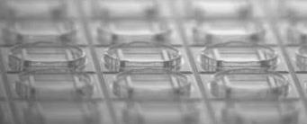
4 Serving high-tech industries Semiconductor Optical Optoelectronic Displays Touch Panels Printed Electronics & PCB Batteries Smart Glass Automotive Photovoltaics High-end solutions for high-tech industries


5 Meyer Burger s Specialized Technologies portfolio Cutting Slicing Ion Beam processing Plasma processing Inkjet Printing Extensive experience in cutting of high quality hard and brittle materials Advanced plasma and ion beam technologies for high-precision coating, structuring and processing of surfaces Innovative, multi-functional inkjet printing for today s and future applications Covering a broad range of applications available in high-end markets


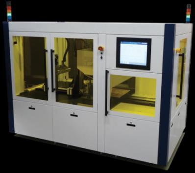
![trimming [nm] IonScan](/docs-images/77/75767753/images/6-5.jpg "Uptime > 95 % at")


6 Meyer Burger enables the future of wireless communication and IoT Thickness correction MEMS MOEMS Frequency trimming BAW SAW Pole trimming TFH pre trimming [nm] post trimming [nm] IonScan Uptime > 95 % at customer side > 50 installed base Reduction of standard deviation σ factor >10 Leading technology to trim surfaces in the 0.1nm range


7 IonScan Technology roadmap edge exclusion electrostatic mechanical Electrostatic clamping Replacing mechanical by electrostatic clamping No edge exclusion No mechanical stress More efficient cooling Increased process area (100%) Less breakage rate (> 99%) Higher uptime Reduced CoO by - 10% New Ionbeam source Redesign of standard source Adjustability of the grid potentials Precise positioning of the grids Robust components Improved long-term stability (+150%) No arcing Less wear of grids Enhanced control and monitoring during process Reduced CoO by - 20%


8 PECVD coating and etching systems Plasma sources Linear Microwave Pulsed DC RF ECR ICP Ion beam Medium scale production and R&D Widespread modular batch or inline system Substrate widths up to 500 mm Scalability processes, components, and technologies Large area, High throughput Industrially proven tray based Inline PECVD equipment SiNA / MAiA / HELiA Installed base > 800 Substrate widths up to 1000 mm Plasma experience for more than 30 years
9 Hardness (GPa) Microwave-PECVD hard coatings (transparent Si 3 N 4 layers) low rate high RF bias 1.9 refractive index n high rate high rate high RF bias no bias 1.8 doped < 1.9 high rate intermediate high rate RF bias no bias Temperature ( C) 400


10 Hardness (GPa) Microwave-PECVD hard coatings (transparent Si 3 N 4 layers) RF-biased enhanced PECVD at T < 100 C low rate high RF bias 1.9 refractive index n Deposition rate > 1.2 nm/s Hardness ~ 15 GPa Low absorption ε < 400 nm Low film stress +100 to -250 MPa for 2 µm high rate high rate high RF bias no bias 1.8 doped < 1.9 high rate intermediate high rate RF bias no bias Good grafting with peel strengths > 1 N On plastics, organics, epoxide resins, copper and tin alloys High breakdown voltage in salty water 20 V/µm Application Hard and scratch-resistant coatings for displays, windows, watches, lenses Insulating barrier layers in electronic devices (e. g. PCBs, panels) under humid condition Temperature ( C)
11 Hardness (GPa) Microwave-PECVD hard coatings (transparent Si 3 N 4 layers) low rate high RF bias 1.9 refractive index n Anti-reflective coatings with SiN x High variability of refractive index of SiN x films (up to 2.2) Low absorption ε < 400 nm high rate high RF bias 1.8 high rate intermediate RF bias high rate no bias doped < 1.9 high rate no bias Temperature ( C) 400 Hardness of up to 16 GPa for doped SiN x Low film stress +100 to -250 MPa Reduction of reflectivity Reflectivity Uncoated Coated Glass 8 % 3 % Sapphire 15 % 3 % Multi Si 27 % 9 % Mono Si 11 % 2 %


12 Microwave Plasma Etch Thin Film and Bulk material Key benefits Well-defined etch depth for typical layer thicknesses 50nm 1000nm Minimizing stress on sample Nitrides Si 3 N 4 Materials Oxides: SiO 2, ZnO, Ta 2 O 5, ITO, Phosphorus glass, Boron glass Silicon a-si, Si cryst., doped Si, et al. Carbon-based Graphit, diamant, organics, et al. Process gases Fluorine-based: NF 3, SF 6, CF 4,... Chlorine-based: N 2 O, Cl2, BCl 3,... Others: H 2, O 2, N 2,... RIE of quartz RIE of Si RIE of GaSb 2
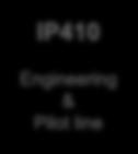


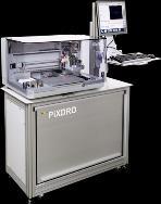

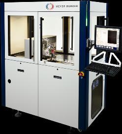

13 Functional Inkjet printing Semiconductors Printed Electronics Displays PCB LP50 R&D IP410 Engineering & Pilot line JETx Mass production Photovoltaics

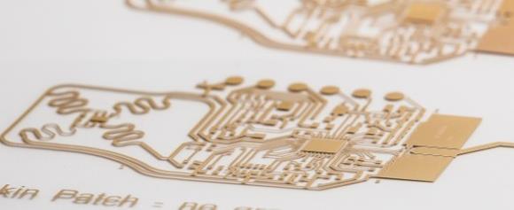
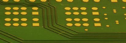
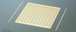
14 Focus applications for Inkjet printing Soldermask Printed Circuit Boards Engineering Versatile Photoresist Dams Semiconductor Pilot Production Flexible Mass Production Efficient Adhesive rqfn \ Flexible Hybrid PE Printed Electronics PV Barriers \


15 Integrated System Solutions Device Encapsulation Barrier for Foil CONx Microfab Complete encapsulation solution Includes plasma and inkjet tools Inert product handling Complete barrier film solution Based on innovative atomic layer deposition Includes foil pre-treatment and organic coating modules Integrated pilot manufacturing line for novel electronics Includes plasma and inkjet tools Integrated product handling and controlled environment


16 Advanced plasma coating Photovoltaics OLED Battery Flex Electronics Glass Application Key figures Process Process material PV OLED Battery Electronics Glass Encapsulation WVTR <1*10-6 g/m 2 /day in/organic coating SiH 4, NH 3, N 2 O, TMA High capacity anode >40% higher capacity amorphous silicon SiH 4, H 2 Etching/Stripping material removal CF 4, NF 3, O 2 Hardening on plastics > 15GPa, with T<100 C inorganic coating SiH 4, NH 3, H 2 AR coating Reflectivity 2% inorganic coating SiH 4, NH 3, H 2, N 2 O...

17 Many thanks for your attention. Visit us at: B and B3-178
18 Properties of selected PECVD- layer Layer typ Typical process Gases Deposition temperature [ C ] Refractive index Band gap [ ev ] Density [ g/cm 3 ] Vickers Hardness [GPa] Dielectric constant Breakdown field [MV/cm] Application Favoured plasma technique SiOx SiH 4 + N 2 O or silicon organics + N 2 O Optics, Electronics, PV Semiconductor, food, hard coating, protection µw, CCP, ETP, ICP SiOxNy SiH 4 + N 2 O + NH 3 or Si org N 2 O + NH 3 SiNx SiH 4 + NH 3 < 150 C SiNx SiH 4 + NH SiCxNy (SiH 4 ) + TMS + NH ? SiCx SiH 4 + CH ? a-si:h SiH 4 + H ? < ? ? PV, glass industry, moisture barrier, Optics, plastics, semiconductor, barrier, PV, Optics, semiconductor, barrier, architecture glass PV, ARC, mech. and chemical protection, PV, LED, sensors, protection, high temperature stable, PV, electronics, TFT, semiconductor. µw, CCP, ETP, ICP µw µw, CCP, ETP CCP, ICP, CCP, ICP µw, CCP, ETP, ICP µc-si:h SiH 4 + H ? ? ? PV, semiconductor, CCP AlOx TMA + N 2 O ? < ? 2-5 a-c:h (DLC) C 2 H 2 + Ar < < Diamond CH 4 + H PV, Optics, semiconductor, Optics, hardcoating, electronics, Electronics, hardcoating, µw, CCP, ETP, ICP CCP µw


19 Vacuum processes for surface modification COATING ETCHING FUNCTIONALISATION IMPLANTATION TREATMENT PECVD MOCVD, ALD, IAD, PICVD IBD, DIBD MSD evaporation (thermal, e- Beam) Reactive and nonreactive RIE, MERIE, ALE Chemical etching IBE, RIBE, CAIBE Change of binding properties of the surfaces Oxidation Nitriding Carbonating Hydrogen-diffusion Radiation (IR, UV) Ionen Implantation PBII PIII Doping Particle interaction with the substrate surface, Physical and/or chemical, Radiation Applications Antireflection, Reflection, Filter Protective coatings Electr. isolation Dielectrics semiconductors Contact-layer Barriere coating Structuring of surfaces of metals, dielectrics, semiconductor e.g. MEMS, Hydrophobic or hydrophilic printing Coloration water absorption hardening Hardening Change of conductivity Buried functional layers semiconductorfunctions (e.g. pnjunctions) Surface activation Improve of adhesion Inerting Germ and bacteria killing Cleaning
Low temperature deposition of thin passivation layers by plasma ALD
 1 Low temperature deposition of thin passivation layers by plasma ALD Bernd Gruska, SENTECH Instruments GmbH, Germany 1. SENTECH in brief 2. Low temperature deposition processes 3. SENTECH SI ALD LL System
Roll-to-roll Technology for Transparent High Barrier Films
 Roll-to-roll Technology for Transparent High Barrier Films Presented at the AIMCAL Fall Technical Conference, October 19-22, 2008, Myrtle Beach, SC, USA Nicolas Schiller, John Fahlteich, Matthias Fahland,
Applied Research for Vacuum Web Coating: What is Coming Next?
 Applied Research for Vacuum Web Coating: What is Coming Next? Matthias Fahland, John Fahlteich, Steffen Günther, Manuela Junghähnel, Claus Luber, Nicolas Schiller, Cindy Steiner, Steffen Straach, Michiel
Flexible functional devices at mass production level with the FLEx R2R sald platform
 Flexible functional devices at mass production level with the FLEx R2R sald platform D. Spee, W. Boonen, D. Borsa and E. Clerkx Meyer Burger (Netherlands) B.V. Meyer Burger Introduction to sald Challenges
Ultra High Barrier Coatings by PECVD
 Society of Vacuum Coaters 2014 Technical Conference Presentation Ultra High Barrier Coatings by PECVD John Madocks & Phong Ngo, General Plasma Inc., 546 E. 25 th Street, Tucson, Arizona, USA Abstract Silicon
Thin film silicon technology. Cosimo Gerardi 3SUN R&D Tech. Coordinator
 Thin film silicon technology Cosimo Gerardi 3SUN R&D Tech. Coordinator 1 Outline Why thin film Si? Advantages of Si thin film Si thin film vs. other thin film Hydrogenated amorphous silicon Energy gap
Atomic Layer Deposition(ALD)
") Atomic Layer Deposition(ALD) AlO x for diffusion barriers OLED displays http://en.wikipedia.org/wiki/atomic_layer_deposition#/media/file:ald_schematics.jpg Lam s market-leading ALTUS systems combine CVD
Atomic Layer Deposition(ALD) AlO x for diffusion barriers OLED displays http://en.wikipedia.org/wiki/atomic_layer_deposition#/media/file:ald_schematics.jpg Lam s market-leading ALTUS systems combine CVD
Micro-Electro-Mechanical Systems (MEMS) Fabrication. Special Process Modules for MEMS. Principle of Sensing and Actuation
 Fabrication. Special Process Modules for MEMS. Principle of Sensing and Actuation") Micro-Electro-Mechanical Systems (MEMS) Fabrication Fabrication Considerations Stress-Strain, Thin-film Stress, Stiction Special Process Modules for MEMS Bonding, Cavity Sealing, Deep RIE, Spatial forming
Micro-Electro-Mechanical Systems (MEMS) Fabrication Fabrication Considerations Stress-Strain, Thin-film Stress, Stiction Special Process Modules for MEMS Bonding, Cavity Sealing, Deep RIE, Spatial forming
Lecture Day 2 Deposition
 Deposition Lecture Day 2 Deposition PVD - Physical Vapor Deposition E-beam Evaporation Thermal Evaporation (wire feed vs boat) Sputtering CVD - Chemical Vapor Deposition PECVD LPCVD MVD ALD MBE Plating
Metallization deposition and etching. Material mainly taken from Campbell, UCCS
 Metallization deposition and etching Material mainly taken from Campbell, UCCS Application Metallization is back-end processing Metals used are aluminum and copper Mainly involves deposition and etching,
Plasma Activated EB-PVD of Titanium and its Compounds by Means of Large Area SAD
 AIMCAL 2005 Myrtle Beach, SC, USA, October 19th, 2005 Plasma Activated EB-PVD of Titanium and its Compounds by Means of Large Area SAD E. Reinhold, C. Steuer VON ARDENNE Anlagentechnik GmbH, Dresden, Germany
LOT. Contents. Introduction to Thin Film Technology. Chair of Surface and Materials Technology
 Introduction to Thin Film Contents 1. Introduction and Application Examples (2h) 2. Preparation of Thin Films by PVD (Physical Vapor Deposition) (6h) 2.1 Vacuum Technique (1h) 2.1.1 Kinetics of Gases 2.1.2
Amorphous Silicon Solar Cells
 The Birnie Group solar class and website were created with much-appreciated support from the NSF CRCD Program under grants 0203504 and 0509886. Continuing Support from the McLaren Endowment is also greatly
Productivity versus Profitability in Vacuum Web Coating
 Productivity versus Profitability in Vacuum Web Coating Liz Josephson, Applied Films Corp., Longmont, USA Dirk Hoffmann, Applied Films GmbH & Co KG, Alzenau, Germany Gerard Loebig, Applied Films GmbH &
Etching Mask Properties of Diamond-Like Carbon Films
 N. New Nawachi Diamond et al. and Frontier Carbon Technology 13 Vol. 15, No. 1 2005 MYU Tokyo NDFCT 470 Etching Mask Properties of Diamond-Like Carbon Films Norio Nawachi *, Akira Yamamoto, Takahiro Tsutsumoto
"Plasma CVD passivation; Key to high efficiency silicon solar cells",
 "Plasma CVD passivation; Key to high efficiency silicon solar cells", David Tanner Date: May 7, 2015 2012 GTAT Corporation. All rights reserved. Summary: Remarkable efficiency improvements of silicon solar
Semiconductor Manufacturing Technology. IC Fabrication Process Overview
 Semiconductor Manufacturing Technology Michael Quirk & Julian Serda October 00 by Prentice Hall Chapter 9 IC Fabrication Process Overview /4 Objectives After studying the material in this chapter, you
R&D ACTIVITIES AT ASSCP-BHEL,GURGAON IN SOLAR PV. DST-EPSRC Workshop on Solar Energy Research
 R&D ACTIVITIES AT -BHEL,GURGAON IN SOLAR PV at the DST-EPSRC Workshop on Solar Energy Research (22 nd 23 rd April, 2009) by Dr.R.K. Bhogra, Addl. General Manager & Head Email: cpdrkb@bhel.co.in Dr.A.K.
A Deep Silicon RIE Primer Bosch Etching of Deep Structures in Silicon
 A Deep Silicon RIE Primer Bosch Etching of Deep Structures in Silicon April 2009 A Deep Silicon RIE Primer 1.0) Etching: Silicon does not naturally etch anisotropically in fluorine based chemistries. Si
Supporting Information
 Supporting Information Fast-Response, Sensitivitive and Low-Powered Chemosensors by Fusing Nanostructured Porous Thin Film and IDEs-Microheater Chip Zhengfei Dai,, Lei Xu,#,, Guotao Duan *,, Tie Li *,,
Etching Etching Definitions Isotropic Etching: same in all direction Anisotropic Etching: direction sensitive Selectivity: etch rate difference
 Etching Etching Definitions Isotropic Etching: same in all direction Anisotropic Etching: direction sensitive Selectivity: etch rate difference between 2 materials Need strong selectivity from masking
EXCIMER LASER ANNEALING FOR LOW- TEMPERATURE POLYSILICON THIN FILM TRANSISTOR FABRICATION ON PLASTIC SUBSTRATES
 EXCIMER LASER ANNEALING FOR LOW- TEMPERATURE POLYSILICON THIN FILM TRANSISTOR FABRICATION ON PLASTIC SUBSTRATES G. Fortunato, A. Pecora, L. Maiolo, M. Cuscunà, D. Simeone, A. Minotti, and L. Mariucci CNR-IMM,
Corrosion Protect DLC Coating on Steel and Hastelloy
 Materials Transactions, Vol. 49, No. 6 (2008) pp. 1333 to 1337 #2008 The Japan Institute of Metals Corrosion Protect DLC Coating on Steel and Hastelloy Hironobu Miya and Jie Wang Semiconductor Equipment
Surface Preparation Challenges in Crystalline Silicon Photovoltaic Manufacturing
 Surface Preparation Challenges in Crystalline Silicon Photovoltaic Manufacturing Kristopher Davis 1,3, Andrew C. Rudack 2,3, Winston Schoenfeld 1,3 Hubert Seigneur 1,3, Joe Walters 1,3, Linda Wilson 2,3
Optical Coatings. Photonics 4 Luxury Coatings , Genève. Dr. Andreas Bächli Head of Optical Coatings at RhySearch, Buchs (SG)
") Optical Coatings Photonics 4 Luxury Coatings 21.06.2017, Genève Dr. Andreas Bächli Head of Optical Coatings at RhySearch, Buchs (SG) RhySearch The Research- and Innovation Center in the Rhine Valley RhySearch
Optical Coatings Photonics 4 Luxury Coatings 21.06.2017, Genève Dr. Andreas Bächli Head of Optical Coatings at RhySearch, Buchs (SG) RhySearch The Research- and Innovation Center in the Rhine Valley RhySearch
Process steps for Field Emitter devices built on Silicon wafers And 3D Photovoltaics on Silicon wafers
 Process steps for Field Emitter devices built on Silicon wafers And 3D Photovoltaics on Silicon wafers David W. Stollberg, Ph.D., P.E. Research Engineer and Adjunct Faculty GTRI_B-1 Field Emitters GTRI_B-2
"ITO Film Trend for Touch Panel Applications"
 AIMCAL Web Coating Conference 2011 October 23-26 Reno, Nevada USA 1 "ITO Film Trend for Touch Panel Applications" Teijin Chemicals Ltd. Haruhiko Itoh 2 Content 1. Structure and Features of TCF 2. Touch
LOW TEMPERATURE PHOTONIC SINTERING FOR PRINTED ELECTRONICS. Dr. Saad Ahmed XENON Corporation November 19, 2015
 LOW TEMPERATURE PHOTONIC SINTERING FOR PRINTED ELECTRONICS Dr. Saad Ahmed XENON Corporation November 19, 2015 Topics Introduction to Pulsed Light Photonic sintering for Printed Electronics R&D Tools for
Isolation of elements
 1 In an IC, devices on the same substrate must be isolated from one another so that there is no current conduction between them. Isolation uses either the junction or dielectric technique or a combination
Turn-key Production System for Solar Cells
 SOLARE Turn-key Production System for Solar Cells 02 Innovations for New Technologies provides technology solutions for both crystalline and thin-film highperformance solar cell platforms. Our production
Microwave Plasma Processing
 Microwave Plasma Processing MUEGGE GMBH Hochstraße 4-6 64385 Reichelsheim Fon +49 (0) 6164-93 07 11 Fax +49 (0) 6164-93 07 93 info@muegge.de www.muegge.de Microwave Plasma Processing Microwave Plasma Technology:
Atomic Oxygen-Resistant, Static-Dissipative, Pinhole-Free Coatings for Spacecraft
 Physical Sciences Inc. VG10-109 Atomic Oxygen-Resistant, Static-Dissipative, Pinhole-Free Coatings for Spacecraft Michelle T. Schulberg, Robert H. Krech, Frederick S. Lauten Physical Sciences Inc. Roy
5.8 Diaphragm Uniaxial Optical Accelerometer
 5.8 Diaphragm Uniaxial Optical Accelerometer Optical accelerometers are based on the BESOI (Bond and Etch back Silicon On Insulator) wafers, supplied by Shin-Etsu with (100) orientation, 4 diameter and
micro resist technology
 Characteristics Processing guidelines Negative Tone Photoresist Series ma-n 2400 ma-n 2400 is a negative tone photoresist series designed for the use in micro- and nanoelectronics. The resists are available
The Effects of Defects on the Moisture-Barrier Performance of Clear Coatings on Polymer Substrates.
 AIMCAL, CHARLESTON, SC, 2013 The Effects of Defects on the Moisture-Barrier Performance of Clear Coatings on Polymer Substrates. The National Centre for Printed Electronics ALF part SMITH of Centre for
IMRE/ETPL Flagship Project
 IMRE/ETPL Flagship Project Nanoparticulate Barrier Films & Gas Permeation Measurement Techniques for Thin Film Solar & Display Application Problems Senthil Ramadas Institute of Materials Research & Engineering
CMOS Manufacturing Process
 CMOS Manufacturing Process CMOS Process A Modern CMOS Process gate-oxide TiSi 2 AlCu Tungsten SiO 2 n+ p-well p-epi poly n-well p+ SiO 2 p+ Dual-Well Trench-Isolated CMOS Process Circuit Under Design V
From Vacuum to Atmosphere and back an in-house Process Chain for Different Products
 From Vacuum to Atmosphere and back an in-house Process Chain for Different Products Dr. Steffen Günther Vacuum coating low pressure 10-1 10-4 Pa (10-3 10-6 mbar) unhindered particle movement no unintended
Preparation and Characterization of Micro-Crystalline Hydrogenated Silicon Carbide p-layers
 Preparation and Characterization of Micro-Crystalline Hydrogenated Silicon Carbide p-layers Erten Eser, Steven S. Hegedus and Wayne A. Buchanan Institute of Energy Conversion University of Delaware, Newark,
Thin Films: Sputtering Systems (Jaeger Ch 6 & Ruska Ch 7,) Can deposit any material on any substrate (in principal) Start with pumping down to high
 Can deposit any material on any substrate (in principal) Start with pumping down to high") Thin Films: Sputtering Systems (Jaeger Ch 6 & Ruska Ch 7,) Can deposit any material on any substrate (in principal) Start with pumping down to high vacuum ~10-7 torr Removes residual gases eg oxygen from
Thin Films: Sputtering Systems (Jaeger Ch 6 & Ruska Ch 7,) Can deposit any material on any substrate (in principal) Start with pumping down to high vacuum ~10-7 torr Removes residual gases eg oxygen from
Processing guidelines
 Processing guidelines mr-uvcur21 series UV-curable Polymer for UV-based Nanoimprint Lithography Characteristics mr-uvcur21 is a liquid UV-curable polymer system with low viscosity and high curing rate
EE40 Lec 22. IC Fabrication Technology. Prof. Nathan Cheung 11/19/2009
 Suggested Reading EE40 Lec 22 IC Fabrication Technology Prof. Nathan Cheung 11/19/2009 300mm Fab Tour http://www-03.ibm.com/technology/manufacturing/technology_tour_300mm_foundry.html Overview of IC Technology
Freshure Coatings: Environmentally Friendly Barrier Coatings
 Freshure Coatings: Environmentally Friendly Barrier Coatings Shahab Jahromi Knowfort Technologies BV Urmonderbaan 20a 6160MD Geleen The Netherlands Email: s.jahromi@knowfort.com Introduction. Roll-to-roll
Photonic Drying Pulsed Light as a low Temperature Sintering Process
 Photonic Drying Pulsed Light as a low Temperature Sintering Process Lou Panico Xenon Corporation W E S T E R N M I C H I G A N U N I V E R S I T Y PRESENTATION OVERVIEW What is Printed Electronics Materials
Energy Efficient Glazing Design. John Ridealgh Off-Line Coatings Technology Group Pilkington European Technology Centre
 Energy Efficient Glazing Design John Ridealgh Off-Line Coatings Technology Group Pilkington European Technology Centre 2 John Ridealgh 30th November 2009 Talk Outline Pilkington Group Limited & NSG Group
Production of PV cells
 Production of PV cells MWp 1400 1200 Average market growth 1981-2003: 32% 2004: 67% 1000 800 600 400 200 0 1991 1992 1993 1994 1995 1996 1997 1998 1999 2000 2001 2002 2003 2004 rest 1.0 1.0 1.0 2.0 4.0
Lecture 8. Deposition of dielectrics and metal gate stacks (CVD, ALD)
") Lecture 8 Deposition of dielectrics and metal gate stacks (CVD, ALD) Thin Film Deposition Requirements Many films, made of many different materials are deposited during a standard CMS process. Gate Electrodes
Lecture 8 Deposition of dielectrics and metal gate stacks (CVD, ALD) Thin Film Deposition Requirements Many films, made of many different materials are deposited during a standard CMS process. Gate Electrodes
High Rate low pressure PECVD for barrier and optical coatings
 High Rate low pressure PECVD for barrier and optical coatings, Matthias Fahland, John Fahlteich, Björn Meyer, Steffen Straach, Nicolas Schiller Outline Introduction PECVD New developments magpecvd arcpecv
Study on Properties of Silicon Oxycarbide Thin Films Prepared by RF Magnetron Sputtering Tao Chen a, Maojin Dong, Jizhou Wang,Ling Zhang and Chen Li
 Study on Properties of Silicon Oxycarbide Thin Films Prepared by RF Magnetron Sputtering Tao Chen a, Maojin Dong, Jizhou Wang,Ling Zhang and Chen Li Science and Technology on Surface Engineering Laboratory,
Plasma..TI'1eITI1 I.P.
 Plasma..TI'1eITI1 I.P. RPPI..ICRTION NOTES PLASMA ETCHING OF SIUCON NITRIDE AND SIUCON DIOXIDE Silicon nitride and silicon dioxide thin films find e variety of uses in both semiconductor and nonsemiconductor
Lecture #9: Active-Matrix LCDs
 Lecture #9: Active-Matrix LCDs Introduction OUTLINE Active-matrix switching elements TFT performance requirements Active matrix processing constraints Amorphous silicon (a-si) TFT technology TFT fabrication
enabling tomorrow s technologies CVD Production Systems for Industrial Coatings powered by
 enabling tomorrow s technologies CVD Production Systems for Industrial Coatings powered by www.cvdequipment.com Equipment Design, Engineering, and Manufacturing Thin film deposition systems for industrial
Amorphous Oxide Transistor Electrokinetic Reflective Display on Flexible Glass
 Amorphous Oxide Transistor Electrokinetic Reflective Display on Flexible Glass Devin A. Mourey, Randy L. Hoffman, Sean M. Garner *, Arliena Holm, Brad Benson, Gregg Combs, James E. Abbott, Xinghua Li*,
Behavior of the parameters of microcrystalline silicon TFTs under mechanical strain. S. Janfaoui*, C. Simon, N. Coulon, T.
 Author manuscript, published in "Solid-State Electronics 93 (2014) 1-7" DOI : 10.1016/j.sse.2013.12.001 Behavior of the parameters of microcrystalline silicon TFTs under mechanical strain S. Janfaoui*,
Coatings. Ion Assisted Deposition (IAD) process Advance Plasma Source (APS) plasma-ion assisted Deposition. Coatings on Optical Fibers
 process Advance Plasma Source (APS) plasma-ion assisted Deposition. Coatings on Optical Fibers") Anti-Reflection Custom Ion Assisted Deposition (IAD) process Advance Plasma Source (APS) plasma-ion assisted Deposition Anti-Reflection on Optical Fibers OptoSigma supplies a wide selection of optical
Anti-Reflection Custom Ion Assisted Deposition (IAD) process Advance Plasma Source (APS) plasma-ion assisted Deposition Anti-Reflection on Optical Fibers OptoSigma supplies a wide selection of optical
CSI G SYSTEMS CSI GAS DELIVERY SUPPORT. Chemical Vapor Deposition (CVD)
") This page discusses the CVD processes often used for integrated circuits (ICs). Particular materials are deposited best under particular conditions. Facilitation recommendations are at the bottom of the
This page discusses the CVD processes often used for integrated circuits (ICs). Particular materials are deposited best under particular conditions. Facilitation recommendations are at the bottom of the
Alternative Methods of Yttria Deposition For Semiconductor Applications. Rajan Bamola Paul Robinson
 Alternative Methods of Yttria Deposition For Semiconductor Applications Rajan Bamola Paul Robinson Origin of Productivity Losses in Etch Process Aggressive corrosive/erosive plasma used for etch Corrosion/erosion
Advances in Intense Pulsed Light Solutions For Display Manufacturing. XENON Corporation Dr. Saad Ahmed Japan IDW 2016
 Advances in Intense Pulsed Light Solutions For Display Manufacturing XENON Corporation Dr. Saad Ahmed Japan IDW 2016 Talk Outline Introduction to Pulsed Light Applications in Display UV Curing Applications
Thin Films: Sputtering Systems (Jaeger Ch 6 & Ruska Ch 7,) Sputtering: gas plasma transfers atoms from target to substrate Can deposit any material
 Sputtering: gas plasma transfers atoms from target to substrate Can deposit any material") Thin Films: Sputtering Systems (Jaeger Ch 6 & Ruska Ch 7,) Sputtering: gas plasma transfers atoms from target to substrate Can deposit any material on any substrate (in principal) Start with pumping down
Thin Films: Sputtering Systems (Jaeger Ch 6 & Ruska Ch 7,) Sputtering: gas plasma transfers atoms from target to substrate Can deposit any material on any substrate (in principal) Start with pumping down
1 Introduction. 2 Basic Technology
 Innovative Clear Barrier Technology for the Packaging Industry Nicolas Schiller 1, Steffen Straach, Steffen Günther Fraunhofer FEP, Germany Alexandra L. Quiceno G., Antonio García Contreras BIOFILM, Columbia
Innovative Laser Processing Technologies
 Innovative Laser Processing Technologies Reinhard Ferstl Director Sales & Marketing EMEA / Asia Corning Laser Technologies September 21, 2016 2016 Corning Incorporated Corning Market Segments and Additional
High strain point glass substrate for photovoltaic solar cell
 Empowering solar efficiency Module material PV200 High strain point glass substrate for photovoltaic solar cell Much less deformation in the heating process than soda-lime glass. Small variations in thermal
Fabrication Technology
 Fabrication Technology By B.G.Balagangadhar Department of Electronics and Communication Ghousia College of Engineering, Ramanagaram 1 OUTLINE Introduction Why Silicon The purity of Silicon Czochralski
ZnO-based Transparent Conductive Oxide Thin Films
 IEEE EDS Mini-colloquium WIMNACT 32 ZnO-based Transparent Conductive Oxide Thin Films Weijie SONG Ningbo Institute of Material Technology and Engineering, Chinese Academy of Sciences, Ningbo, P. R. China
Processing guidelines. Negative Tone Photoresist Series ma-n 2400
 Characteristics Processing guidelines Negative Tone Photoresist Series ma-n 2400 ma-n 2400 is a negative tone photoresist series designed for the use in micro- and nanoelectronics. The resists are available
Barix Multilayers: a Water and Oxygen Barrier for Flexible Organic Electronics. Robert Jan Visser
 Barix Multilayers: a Water and Oxygen Barrier for Flexible Organic Electronics Robert Jan Visser Organic Electronics Is the Future of Electronics Organic? MIT Stanford UC Berkeley Nano Forum Vitex Systems,
Silicon Wafer Processing PAKAGING AND TEST
 Silicon Wafer Processing PAKAGING AND TEST Parametrical test using test structures regularly distributed in the wafer Wafer die test marking defective dies dies separation die fixing (not marked as defective)
A hollow cathode high density plasma process for internally coating cylindrical substrates
 A hollow cathode high density plasma process for internally coating cylindrical substrates D. Lusk, M. Gore Sub-One Europe Ltd., The Exchange No 1, 5 th Aberdeen, Scotland, AB11 5PJ Floor, 62 Market Street,
Isolation Technology. Dr. Lynn Fuller
 ROCHESTER INSTITUTE OF TECHNOLOGY MICROELECTRONIC ENGINEERING Isolation Technology Dr. Lynn Fuller Motorola Professor 82 Lomb Memorial Drive Rochester, NY 14623-5604 Tel (585) 475-2035 Fax (585) 475-5041
c/bach, 2-B Pol. Ind Foinvasa Montcada i Reixac (Barcelona) SPAIN Tel FAX
 SPAIN Tel FAX") 1- What is 2- How does it work? 3- How do we make it? 4- Applications 5- Processing? WHAT IS? Thick aluminium based substrate, cladded in ED copper foil. Designed for an effective thermal dissipation and
1- What is 2- How does it work? 3- How do we make it? 4- Applications 5- Processing? WHAT IS? Thick aluminium based substrate, cladded in ED copper foil. Designed for an effective thermal dissipation and
Vacuum plasma treatment and coating of fluoropolymer webs challenges and applications
 Vacuum plasma treatment and coating of fluoropolymer webs challenges and applications AIMCAL 2016 Cindy Steiner John Fahlteich Dresden, 01.06.2016 page 1 Ethylene Tetrafluoroethylene (ETFE) semi-crystalline
Metallization. Typical current density ~10 5 A/cm 2 Wires introduce parasitic resistance and capacitance
 Metallization Interconnects Typical current density ~10 5 A/cm 2 Wires introduce parasitic resistance and capacitance RC time delay Inter-Metal Dielectric -Prefer low dielectric constant to reduce capacitance
Surface micromachining and Process flow part 1
 Surface micromachining and Process flow part 1 Identify the basic steps of a generic surface micromachining process Identify the critical requirements needed to create a MEMS using surface micromachining
Laser Micromachining for Industrial Applications and R&D. 3D-Micromac AG. Symposium on Smart Integrated Systems in Chemnitz. 3D-Micromac AG
 3D-Micromac AG Symposium on Smart Integrated Systems in Chemnitz 1 1 microdice - TLS-Dicing for separation of SiC 2 microprep - for high-throughput microstructure diagnostics 3 About 3D-Micromac AG 2 microdice
AC Reactive Sputtering with Inverted Cylindrical Magnetrons
 AC Reactive Sputtering with Inverted Cylindrical Magnetrons D.A. Glocker, Isoflux Incorporated, Rush, NY; and V.W. Lindberg and A.R. Woodard, Rochester Institute of Technology, Rochester, NY Key Words:
Procese de depunere in sistemul Plasma Enhanced Chemical Vapor Deposition (PECVD)
") Procese de depunere in sistemul Plasma Enhanced Chemical Vapor Deposition (PECVD) Ciprian Iliescu Conţinutul acestui material nu reprezintă in mod obligatoriu poziţia oficială a Uniunii Europene sau a
Procese de depunere in sistemul Plasma Enhanced Chemical Vapor Deposition (PECVD) Ciprian Iliescu Conţinutul acestui material nu reprezintă in mod obligatoriu poziţia oficială a Uniunii Europene sau a
April 17 19, Forum is part financed by Podlaskie Region
 Suwałki, POLAND April 17 19, 2013 Optimization of device construction and deposition technology of ta-c coatings using Taguchi method of experiment design Viktor Zavaleyev Koszalin University of Technology(Poland/Ukraine)
CYRANNUS. Welcome at iplas. See the latest developments! CYRANNUS.
 Welcome at iplas. See the latest developments! High performance plasma CYlindrical Resonator with ANNUlar Slots EH-tuner from vacuum to atmosphere uniform plasma large plasma extension high power density
Introduction to Micro/Nano Fabrication Techniques. Date: 2015/05/22 Dr. Yi-Chung Tung. Fabrication of Nanomaterials
 Introduction to Micro/Nano Fabrication Techniques Date: 2015/05/22 Dr. Yi-Chung Tung Fabrication of Nanomaterials Top-Down Approach Begin with bulk materials that are reduced into nanoscale materials Ex:
Thermal Evaporation. Theory
 Thermal Evaporation Theory 1. Introduction Procedures for depositing films are a very important set of processes since all of the layers above the surface of the wafer must be deposited. We can classify
Surface Micromachining
 Surface Micromachining Outline Introduction Material often used in surface micromachining Material selection criteria in surface micromachining Case study: Fabrication of electrostatic motor Major issues
TUTORIAL ON SPUTTER DEPOSITION
 MATERION ADVANCED CHEMICALS COATING MATERIALS NEWS September 2011 Volume 22 Issue 1 TUTORIAL ON SPUTTER DEPOSITION NEW ON THE WEB Non-Silicon Thin-Film PV Materials Progress and Challenges by - David A.
Vacuum deposition of TiN
 J.Lorkiewicz DESY.27.10.02 Vacuum deposition of TiN (TiN coating of high power coupler elements as an anti-multipactor remedy at DESY) The scope of the project: - reducing secondary electron emission and
Nonplanar Metallization. Planar Metallization. Professor N Cheung, U.C. Berkeley
 Nonplanar Metallization Planar Metallization Passivation Metal 5 (copper) Metal 3 (copper) Interlevel dielectric (ILD) Via (tungsten) Metal 1 (copper) Tungsten Plug to Si Silicon Caps and Plugs oxide oxide
School of Photovoltaic and Renewable Energy Engineering
 School of Photovoltaic and Renewable Energy Engineering Silicon PV Education, Research and Industry in Australia R. Corkish, Head of School r.corkish@unsw.edu.au www.pv.unsw.edu.au Photo: K. McLean Context:
Oxide Growth. 1. Introduction
 Oxide Growth 1. Introduction Development of high-quality silicon dioxide (SiO2) has helped to establish the dominance of silicon in the production of commercial integrated circuits. Among all the various
Solar Film Introduction. Company Presentation 1
 olar Film Introduction Company Presentation 1 Executive ummary Background pecialized in the production of organic solar films based on proprietary IP Founded in 2006 out of two leading universities HQ
Nanoscale Barrier Coating on BOPP Packaging Film by ALD Presented by: Dr. Johanna Lahti Senior Research Fellow Tampere University of Technology
 Nanoscale Barrier Coating on BPP Packaging Film by ALD Presented by: Dr. Johanna Lahti Senior Research Fellow Tampere University of Technology Co-authors: Kimmo Lahtinen (LUT*), Petri Johansson (TUT),
Atomic Layer Deposition
 Atomic Layer Deposition Ville Malinen R&D Engineer Nanopinnoitteita koneenrakentajille 2010 1 Introduction 1) Overview of Beneq 2) Atomic Layer Deposition (ALD), to deposit thin films, which Are dense
R Sensor resistance (Ω) ρ Specific resistivity of bulk Silicon (Ω cm) d Diameter of measuring point (cm)
 ρ Specific resistivity of bulk Silicon (Ω cm) d Diameter of measuring point (cm)") 4 Silicon Temperature Sensors 4.1 Introduction The KTY temperature sensor developed by Infineon Technologies is based on the principle of the Spreading Resistance. The expression Spreading Resistance derives
4 Silicon Temperature Sensors 4.1 Introduction The KTY temperature sensor developed by Infineon Technologies is based on the principle of the Spreading Resistance. The expression Spreading Resistance derives
200mm Next Generation MEMS Technology update. Florent Ducrot
 200mm Next Generation MEMS Technology update Florent Ducrot The Most Exciting Industries on Earth Semiconductor Display Solar 20,000,000x reduction in COST PER TRANSISTOR in 30 years 1 20x reduction in
Lecture 19 Microfabrication 4/1/03 Prof. Andy Neureuther
 EECS 40 Spring 2003 Lecture 19 Microfabrication 4/1/03 Prof. ndy Neureuther How are Integrated Circuits made? Silicon wafers Oxide formation by growth or deposition Other films Pattern transfer by lithography
Linear Plasma Sources for Surface Modification and Deposition for Large Area Coating
 Linear Plasma Sources for Surface Modification and Deposition for Large Area Coating Dr Tony Williams Gencoa Ltd, UK Victor Bellido-Gonzalez, Dr Dermot Monaghan, Dr Joseph Brindley, Robert Brown SVC 2016,
Cu Wiring Process for TFTs - Improved Hydrogen Plasma Resistance with a New Cu Alloy -
 Cu Wiring Process for TFTs - Improved Hydrogen Plasma Resistance with a New Cu Alloy - Masanori Shirai*, Satoru Takazawa*, Satoru Ishibashi*, Tadashi Masuda* As flat-screen TVs become larger and their
Fabrication and STM Nanostructuring of tetrahedral amorphous Carbon. Teja Roch
 Fabrication and STM Nanostructuring of tetrahedral amorphous Carbon Teja Roch Fabrication and STM Nanostructuring of tetrahedral amorphous Carbon (ta-c) Content: Who are we? What are we doing? Why are
Semiconductor Technology
 Semiconductor Technology von A bis Z Metallization www.halbleiter.org Contents Contents List of Figures List of Tables II III 1 Metallization 1 1.1 Requirements on metallization........................
and Technology of Thin Films
 An Introduction to Physics and Technology of Thin Films This page is intentionally left blank An Introduction to Physics and Technology of Thin Films Alfred Wagendriste1 Institute of Applied and Technical
Anodic Aluminium Oxide for Passivation in Silicon Solar Cells
 Anodic Aluminium Oxide for Passivation in Silicon Solar Cells School of Photovoltaic & Renewable Energy Engineering Zhong Lu Supervisor: Alison Lennon May. 2015 Co-supervisor: Stuart Wenham Outline Introduction
Materials for MEMS. Dr. Yael Hanein. 11 March 2004 Materials Applications Yael Hanein
 Materials for MEMS Dr. Yael Hanein Materials for MEMS MEMS (introduction) Materials used in MEMS Material properties Standard MEMS processes MEMS The world s smallest guitar is about 10 micrometers long
Advanced Sheet-to-Sheet and Roll-to-Roll thin-film processing on ultra-thin flexible glass for flexible electronic devices
 Advanced Sheet-to-Sheet and Roll-to-Roll thin-film processing on ultra-thin flexible glass for flexible electronic devices M. Junghaehnel 1, J. Westphalen 1, F. Naumann 2, G. Lorenz 2, M. Fahland 1, S.