Analog & MEMS Group (AMS)
|
|
|
- Denis Bishop
- 6 years ago
- Views:
Transcription
1 16-March-2017 Report ID 2018-W11 SO16-SHZ PRODUCT/PROCESS CHANGE NOTIFICATION PCN AMS/18/10777 Analog & MEMS Group (AMS) Qualification of ST Shenzhen as Assembly and Test & Finishing site for selected products of General Purpose Analog and Industrial & Power Conversion Divisions in SO16 package March
2 WHAT: Progressing on activities related to production rationalization and capacity increase, ST is pleased to announce the qualification of some IPC (Industrial & Power Conversion) and GPA (General Purpose Analog) products in ST Shenzhen. Please find more information related to the transfer of the impacted products: Material Current process Modified process Comment Diffusion location No change No change Assembly location ST Bouskoura Amkor Philippines (TSM104) ST Shenzhen Amkor Philippines (TSM104) Test location ST Bouskoura ST Shenzhen Molding compound Hitachi MP8000 No change for TSM104 Sumitomo G630AY Sumitomo G700K (ST8034) Die attach HITACHI EN4900 ST10 No change for TSM104 ABLESTIK 8601S-25 ABLESTIK 8601S-25 (ST8034) Lead frame Copper 85x85mils(ST8034) No change for TSM104 Copper 94x150 Copper 94x125 Copper 94x200 (TSM102) Copper 94x160 (TSM102) Wire Gold wire 1mil No change for TSM104 Copper wire 1 mil Copper wire 1 mil (ST8034) Plating Preplated e4 No change MSL No change No change Samples of vehicle test are available now and other samples will be launched upon customer s requests. Please submit requests for samples within 30 days of this notification. WHY: The purpose of the transfer is to rationalize our production tool and increase capacity. HOW: The qualification is based on representative Test vehicles, using internal ST rules for changes. To validate the change, dedicated engineering trials have been performed and reliability report is attached. IMPACTS OF THE CHANGE: Form/Fit/Fonction : No change WHEN: For all impacted products, estimated 1st shipment start date is wk

3 Marking and traceability: Unless otherwise stated by customer s specific requirement, the traceability of the parts assembled with the new material set will be ensured by new internal sales type, date code and lot number. The changes here reported will not affect the electrical, dimensional and thermal parameters keeping unchanged all the information reported on the relevant datasheets. There is -as well- no change in the packing process or in the standard delivery quantities. Lack of acknowledgement of the PCN within 30 days will constitute acceptance of the change. After acknowledgement, lack of additional response within the 90 day period will constitute acceptance of the change (Jedec Standard No. 46-C). Shipments may start earlier with the customer s written agreement. On tracecode PP code will move from CZ (ST Bouskoura) to GK (ST Shenzhen) 7
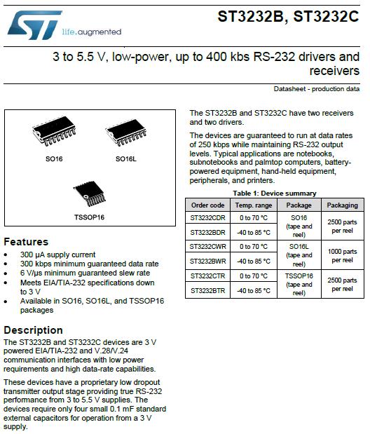
4 Reliability Report Qualification of ST Shenzhen as Assembly and Test & Finishing site for selected products of GPA and IPC Divisions in SO16 package General Information Product Line UI87, 0102, UW55 16-pin smartcard interfaces, VOLTAGE AND CURRENT Product Description CONTROLLER, 3 to 5.5 V, low-power, up to 400 kbs RS- 232 drivers and receivers, ST8034TDT, TSM102/A, P/N ST3232B Product Group AMS General Purpose Analog &RF, Product division Industrial Power Conversion Package SO16 Silicon Process technology BCD6S, Bipolar, BCD3S, Wafer fab Assembly plant Reliability Lab Locations ST Singapore, ST Agrate, ST Catania ST Shenzhen ST Grenoble, ST Casteletto, ST Catania ST Shenzhen Note: This report is a summary of the reliability trials performed in good faith by STMicroelectronics in order to evaluate the potential reliability risks during the product life using a set of defined test methods. This report does not imply for STMicroelectronics expressly or implicitly any contractual obligations other than as set forth in STMicroelectronics general terms and conditions of Sale. This report and its contents shall not be disclosed to a third party without previous written agreement from STMicrolectronics. 8
5 TABLE OF CONTENTS 1 APPLICABLE AND REFERENCE DOCUMENTS GLOSSARY RELIABILITY EVALUATION OVERVIEW OBJECTIVES CONCLUSION DEVICE CHARACTERISTICS DEVICE DESCRIPTION CONSTRUCTION NOTE TESTS RESULTS SUMMARY TEST VEHICLE TEST PLAN AND RESULTS SUMMARY TESTS DESCRIPTION
6 1 APPLICABLE AND REFERENCE DOCUMENTS 16-March Report ID 2018-W11 SO16-SHZ Document reference Short description JESD47 Stress-Test-Driven Qualification of Integrated Circuits Reliability tests and criteria for qualifications 2 GLOSSARY DUT PCB SS Device Under Test Printed Circuit Board Sample Size 3 RELIABILITY EVALUATION OVERVIEW 3.1 Objectives To qualify SO16 package in ST Shenzhen for General purpose analog and Industrial & Power Conversion products. 3.2 Conclusion Qualification Plan requirements will have to be fulfilled without issue. It is stressed that reliability tests have to show that the devices behave correctly against environmental tests (no failure). Moreover, the stability of electrical parameters during the accelerated tests have to demonstrate the ruggedness of the products and safe operation, which is consequently expected during their lifetime. 10

7 4 DEVICE CHARACTERISTICS 4.1 Device description 11
8 12
9 13
10 4.2 Construction note P/N ST8034TDT Wafer/Die fab. information P/N TSM102/A P/N ST 3232B Wafer fab manufacturing location ST Catania ST Singapore ST Singapore Technology BCD6S Bipolar BCD3S Die finishing back side RAW SILICON RAW SILICON Lapped SILICON Die size (microns) 1608x1700 µm 1860x3400µm 1820x2380µm² Bond pad metallization layers AlCu AlSiCu AlSiCu Passivation type TEOS/SiN/Polyimide SiN USG-PSG-SiON- PIX Assembly information Assembly site Package description Molding compound Frame material Die attach process ST Shenzhen SO16 Sumitomo G630AY Copper Glue Die attach material Ablestick 8601 S25 Wire bonding process Tehrmosonic ball bonding Wires bonding materials/diameters Cu 1 mil Lead finishing process Preplated Lead finishing/bump solder material NiPdAu 14
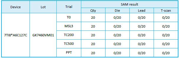
 2 Bipolar /SO16 0102 TSM102/A (lot GK8022FH01) 3 BCD3S/SO16 UW55 ST3232B (lot GK7460VM01) 5.")
11 5 TESTS RESULTS SUMMARY 5.1 Test vehicle Lot # Process/ Package Product Line Comments 1 BCD6S / SO16 UI87 ST8034 (lot GK7510KX01) 2 Bipolar /SO TSM102/A (lot GK8022FH01) 3 BCD3S/SO16 UW55 ST3232B (lot GK7460VM01) 5.2 Test plan and results summary Test PC Std ref. Conditions SS Steps Die oriented tests HTB/ HTOL HTSL N N JESD22 A-108 JESD22 A-103 Ta = 125 C, BIAS Ta = 150 C Lot1 UI H 500 H 1000 H 168 H 0/100 0/80 0/ H 0/100 0/80 0/ H On going On going 0/77 Failure/SS Lot 2 Lot 3 Note Package Oriented Tests PC AC TC Y Y JESD22 A-113 JESD22 A-102 JESD22 A-104 Drying C JL1 (Store 168 Ta=85 C Rh=85%) JL2 (Store 192 Ta=30 C Rh=60%) Over Tpeak=260 C 3 times Pa=2Atm / Ta=121 C Ta = -65 C to 150 C Final PASS MSLS3 MSL3 96 H 0/80 0/80 0/77 168h 200 cy 0/80 0/80 0/ cy 0/80 On going 0/ cy THB Y JESD22 A-101 Ta = 85 C, RH = 85%, BIAS 168 H 500 H 1000 H Scanning acoustic microscopy, check for delamination at die/resin interface, Lead/Resin interface and in through scan: UI87 15
12 UW55 16
13 5.3 Tests Description Test name Description Purpose Die Oriented HTOL High Temperature Operating Life HTB High Temperature Bias HTRB High Temperature Reverse Bias HTFB / HTGB High Temperature Forward (Gate) Bias HTSL High Temperature Storage Life ELFR Early Life Failure Rate Package Oriented PC Preconditioning AC Auto Clave (Pressure Pot) TC Temperature Cycling The device is stressed in static or dynamic configuration, approaching the operative max. absolute ratings in terms of junction temperature and bias condition. The device is stressed in static configuration, trying to satisfy as much as possible the following conditions: low power dissipation; max. supply voltage compatible with diffusion process and internal circuitry limitations; The device is stored in unbiased condition at the max. temperature allowed by the package materials, sometimes higher than the max. operative temperature. The device is stressed in biased conditions at the max junction temperature. The device is submitted to a typical temperature profile used for surface mounting devices, after a controlled moisture absorption. The device is stored in saturated steam, at fixed and controlled conditions of pressure and temperature. The device is submitted to cycled temperature excursions, between a hot and a cold chamber in air atmosphere. To determine the effects of bias conditions and temperature on solid state devices over time. It simulates the devices operating condition in an accelerated way. The typical failure modes are related to, silicon degradation, wire-bonds degradation, oxide faults. To determine the effects of bias conditions and temperature on solid state devices over time. It simulates the devices operating condition in an accelerated way. To maximize the electrical field across either reverse-biased junctions or dielectric layers, in order to investigate the failure modes linked to mobile contamination, oxide ageing, layout sensitivity to surface effects. To investigate the failure mechanisms activated by high temperature, typically wirebonds solder joint ageing, data retention faults, metal stress-voiding. To evaluate the defects inducing failure in early life. As stand-alone test: to investigate the moisture sensitivity level. As preconditioning before other reliability tests: to verify that the surface mounting stress does not impact on the subsequent reliability performance. The typical failure modes are "pop corn" effect and delamination. To investigate corrosion phenomena affecting die or package materials, related to chemical contamination and package hermeticity. To investigate failure modes related to the thermo-mechanical stress induced by the different thermal expansion of the materials interacting in the die-package system. Typical failure modes are linked to metal displacement, dielectric cracking, molding compound delamination, wire-bonds failure, die-attach layer degradation. 17
14 Test name Description Purpose TF / IOL Thermal Fatigue / Intermittent Operating Life THB Temperature Humidity Bias Other ESD Electro Static Discharge LU Latch-Up The device is submitted to cycled temperature excursions generated by power cycles (ON/OFF) at T ambient. The device is biased in static configuration minimizing its internal power dissipation, and stored at controlled conditions of ambient temperature and relative humidity. The device is submitted to a high voltage peak on all his pins simulating ESD stress according to different simulation models. CBM: Charged Device Model HBM: Human Body Model MM: Machine Model The device is submitted to a direct current forced/sunk into the input/output pins. Removing the direct current no change in the supply current must be observed. To investigate failure modes related to the thermo-mechanical stress induced by the different thermal expansion of the materials interacting in the die-package system. Typical failure modes are linked to metal displacement, dielectric cracking, molding compound delamination, wire-bonds failure, die-attach layer degradation. To evaluate the package moisture resistance with electrical field applied, both electrolytic and galvanic corrosion are put in evidence. To classify the device according to his susceptibility to damage or degradation by exposure to electrostatic discharge. To verify the presence of bulk parasitic effect inducing latch-up. 18
Analog, MEMS and Sensor Group (AMS)
") 05-13-2015 Report ID 2015-W20AMKOR-TRANSFER PRODUCT/PROCESS CHANGE NOTIFICATION PCN AMS/15/9324 Analog, MEMS and Sensor Group (AMS) Production transfer from Amkor Korea to Amkor Philippines for component
05-13-2015 Report ID 2015-W20AMKOR-TRANSFER PRODUCT/PROCESS CHANGE NOTIFICATION PCN AMS/15/9324 Analog, MEMS and Sensor Group (AMS) Production transfer from Amkor Korea to Amkor Philippines for component
Analog & MEMS Group (AMG)
") 10-May-2016 Report ID 2016-W18 -SOAG PRODUCT/PROCESS CHANGE NOTIFICATION PCN AMG/16/9830 Analog & MEMS Group (AMG) New material set in ST Bouskoura for General Purpose Analog Automotive grade products
10-May-2016 Report ID 2016-W18 -SOAG PRODUCT/PROCESS CHANGE NOTIFICATION PCN AMG/16/9830 Analog & MEMS Group (AMG) New material set in ST Bouskoura for General Purpose Analog Automotive grade products
PRODUCT/PROCESS CHANGE NOTIFICATION
 PRODUCT/PROCESS CHANGE NOTIFICATION PCN IPD-IPC/13/7708 Dated 19 Feb 2013 VFQFPN/DFN line transfer from ST Muar (Malaysia) to ST Calamba (Philippines) 1/5 PCN IPD-IPC/13/7708 - Dated 19 Feb 2013 Table
PRODUCT/PROCESS CHANGE NOTIFICATION
 PRODUCT/PROCESS CHANGE NOTIFICATION PCN IPG-DIS/14/8337 Dated 19 Feb 2014 Power Rectifiers Additional Assembly and Test Location in China for DPAK package 1/17 PCN IPG-DIS/14/8337 - Dated 19 Feb 2014 Table
Quality and Reliability Report
 Quality and Reliability Report Product Qualification MASW-007921 2mm 8-Lead Plastic Package QTR-0148 M/A-COM Technology Solutions Inc. 100 Chelmsford Street Lowell, MA 01851 Tel: (978) 656-2500 Fax: (978)
Quality and Reliability Report
 Quality and Reliability Report Product Qualification MAAM-008819 2mm 8-Lead PDFN Plastic Package QTR-0147 M/A-COM Technology Solutions Inc. 100 Chelmsford Street Lowell, MA 01851 Tel: (978) 656-2500 Fax:
WorkShop Audace. INSA ROUEN 8 juin 2012
 WorkShop Audace INSA ROUEN 8 juin 2012 Global Standards for the Microelectronics Industry JEDEC standards for product level qualification Christian Gautier Content JEDEC overview Environmental reliability
PRODUCT/PROCESS CHANGE NOTIFICATION
 PRODUCT/PROCESS CHANGE NOTIFICATION PCN MMS-MMY/14/8744 Dated 21 Oct 2014 CR95HF, Redesign for improvement 1/5 PCN MMS-MMY/14/8744 - Dated 21 Oct 2014 Table 1. Change Implementation Schedule Forecasted
PRODUCT/PROCESS CHANGE NOTIFICATION
 PRODUCT/PROCESS CHANGE NOTIFICATION PCN IPG/14/8597 Dated 17 Jul 2014 TO-220FP and DO-220FP Back-End line relocation from Longgang to Shenzhen (China) 1/30 PCN IPG/14/8597 - Dated 17 Jul 2014 Table 1.
Quality and Reliability Report Fourth Quarter 2012 Isolator Products Document ID:
 Quality and Reliab bility Report Fourth Quarte er 212 Isolator Products Docent ID:.doc Note: Alll rights reserved. No part of this publication may be reproduced or transmitted withoutt prior approval by
Qualification Report CASCADEABLE FIFOS. November 1995, QTP# Version 1.2 DEVICE DESCRIPTION MARKETING PART NUMBER. 1K x 9 Cascadeable FIFO
 Qualification Report November 1995, QTP# 94468 Version 1.2 CASCADEABLE FIFOS MARKETING PART NUMBER CY7C419 CY7C420/CY7C421 CY7C424/CY7C425 DEVICE DESCRIPTION 256 x 9 Cascadeable FIFO 512 x 9 Cascadeable
Automotive AEC-Q100 Grade 2 Compliance
 Automotive AEC-Q100 Grade 2 Compliance Reliability Qualification Report for SDR SDRAM with Pb/Halogen Free (4M 16, 63nm SDRAM AS4C4M16SA-6TAN/6BAN) Issued Date: Dec 15, 2014 1 CONTENTS 0. RELIABILITY TEST
CONTENTS 0. RELIABILITY TEST SUMMARY INTRODUCTION PRODUCT INFORMATION RELIABILITY...2
 Reliability Qualification Report for DDR SDRAM with Pb/Halogen Free (Industrial) (64M 8, 45nm SDRAM AS4C64M8D1-5TIN-5BIN) Issued Date: April 18, 2014 Alliance Memory Inc. 511 Taylor Way, San Carlos, CA
Qualification Report. PALCE16V8 (Flash Erasable, Reprogramable CMOS PAL ) April 1996, QTP# 96023, Version 1.0
 April 1996, QTP# 96023, Version 1.0") Qualification Report April 1996, QT# 96023, Version 1.0 ALCE16V8 (Flash Erasable, Reprogramable CMOS AL ) AL is registered trademark of Advanced Micro Devices, Inc. RODUCT DESCRITION (for qualification)
Qualification Report April 1996, QT# 96023, Version 1.0 ALCE16V8 (Flash Erasable, Reprogramable CMOS AL ) AL is registered trademark of Advanced Micro Devices, Inc. RODUCT DESCRITION (for qualification)
Copper Wire Packaging Reliability for Automotive and High Voltage
 Copper Wire Packaging Reliability for Automotive and High Voltage Tu Anh Tran AMPG Package Technology Manager Aug.11.2015 TM External Use Agenda New Automotive Environments Wire Bond Interconnect Selection
PRODUCT/PROCESS CHANGE NOTIFICATION
 PRODUCT/PROCESS CHANGE NOTIFICATION PCN APG-PTS/12/7486 Dated 2 Oct 212 COPPER WIRE CONVERSION ON BCD2 - PowerSO-2/36 MUAR 1/15 PCN APG-PTS/12/7486 - Dated 2 Oct 212 Table 1. Change Implementation Schedule
PRODUCT/PROCESS CHANGE NOTIFICATION
 PRODUCT/PROCESS CHANGE NOTIFICATION PCN APG-BAD/12/7546 Dated 05 Nov 2012 VIPower Products Housed in DPAK/D2PAK,PACK/P2PAK,PENTAWATT: Migration to Leadfree 1/41 PCN APG-BAD/12/7546 - Dated 05 Nov 2012
Qualification Report. June, 1994, QTP# Version 1.1 CY7C46X/47X, MINNESOTA FAB MARKETING PART NUMBER DEVICE DESCRIPTION. Cascadable 32K x 9 FIFO
 Qualification Report June, 1994, QTP# 92361 Version 1.1 CY7C46X/47X, MINNESOTA FAB MARKETING PART NUMBER CY7C460 CY7C462 CY7C464 CY7C470 CY7C472 CY7C474 DEVICE DESCRIPTION Cascadable 8K x 9 FIFO Cascadable
JEDEC SOLID STATE TECHNOLOGY ASSOCIATION
 JEDEC STANDARD Stress-Test-Driven Qualification of Integrated Circuits JESD47G (Revision of JESD47F, December 2007) MARCH 2009 JEDEC SOLID STATE TECHNOLOGY ASSOCIATION NOTICE JEDEC standards and publications
Standard for handling, packing, shipping and use of moisture/reflow sensitive surface mount devices
 This is a preview - click here to buy the full publication,(&3$6 Edition 1.0 2000-08 Standard for handling, packing, shipping and use of moisture/reflow sensitive surface mount devices 38%/,&/
EPC GaN Transistor Application Readiness: Phase Two Testing
 EPC GaN Transistor Application Readiness: EFFICIENT POWER CONVERSION Yanping Ma PhD, Director of Quality and Reliability, Efficient Power Conversion Corporation Efficient Power Conversion Corporation s
GaAs IC Reliability in Plastic Packages
 William J. Roesch and Anthony L. Rubalcava TriQuint Semiconductor, Inc., 3625A S.W. Murray Blvd., Beaverton, Oregon 97005 Phone: 644-3535 ext. 273 FAX: (503) 644-3198 EMail: BillR@TQS.COM Introduction:
PROCESS CHANGE NOTIFICATION PCN1801
 Revision 1.0.0 PCN Issue Date: 01/26/2018 PROCESS CHANGE NOTIFICATION PCN1801 Capillary for Thermal Composite Flip Chip Ball Grid Array (BGA) Packages on Selected Arria II GX and Arria V Devices Change
SOT-23 Reliability November 23, 1998
 SOT-23 Reliability SOT-23 Reliability November 23, 1998 By David B. Hutchins, Senior Applications Engineer Diodes Incorporated -- www.diodes.com Introduction Diodes Incorporated has offered high-quality
Cypress Semiconductor Package Qualification Report
 Cypress Semiconductor Package Qualification Report QTP# 041007 VERSION 1.0 September 2004 28Ld SNC, 32Ld SOIC, 28/32/36/44Ld SOJ Packages 11 mils Wafer Thickness and Saw Step Cut MSL 3, 220C Reflow Cypress
3.0x2.0mm SMD LED WITH CERAMIC SUBSTRATE. PRELIMINARY SPEC Part Number: AT3020QB24ZS-RV Blue. Features. Material as follows: Package Dimensions
 PRELIMINARY SPEC Part Number: AT3020QB24ZS-RV Blue ATTENTION OBSERVE PRECAUTIONS FOR HANDLING ELECTROSTATIC DISCHARGE SENSITIVE DEVICES Features 1.Dimensions : 3.0mm X 2.0mm X 0.8mm. 2.Higher brightness.
Topview 5630 Red SMD LED
 Topview 5630 Red SMD LED 1. Features - Chip High-Luminosity SMD LED - 5.6 x 3.0 x 0.9 mm (L x W x H), 4-Pin, Small Size Surface Mount Type - Wide Viewing Angle - Long Operating Life - MSL 3 2. Applications
Component Palladium Lead Finish - Specification Approved by Executive Board 1997-xx-xx August 22 Version
 Component Palladium Lead Finish - Specification Approved by Executive Board 1997-xx-xx August 22 Version Appendices 1. User Commitment Form 2. Supplier Compliance Form Table of contents 1. Background 2.
Reliability Qualification Report
 Reliability SUF-1000 SUF-2000 SUF-3000 SUF-4000 SUF-5000 The information provided herein is believed to be reliable at press time. Sirenza Microdevices assumes no responsibility for inaccuracies or omissions.
Lattice ispmach 4000 V/B/C/ZC/ZE Product Family Qualification Summary
 Lattice ispmach 4000 V/B/C/ZC/ZE Product Family Qualification Summary Lattice Document # 25-105900 October 2012 2012 Lattice Semiconductor Corp. All Lattice trademarks, registered trademarks, patents,
White Paper Quality and Reliability Challenges for Package on Package. By Craig Hillman and Randy Kong
 White Paper Quality and Reliability Challenges for Package on Package By Craig Hillman and Randy Kong Background Semiconductor technology advances have been fulfilling Moore s law for many decades. However,
SE2618F with Cu wire at Carsem Package Qualification Plan
 SE2618F with Cu wire at Carsem Package Qualification Plan Part Number: SE2618F with Cu wire Product Type: 2.4GHz 802.11b/g/n WLAN FEM Package Type: QFN 2.5 x 2.5 x 0.45mm 16L Report No: Qual-QP-12-01106
What is and what is not changing? Primary Fab Location: Microchip Fabrication Sites (Tempe, AZ and Gresham, OR, USA)
") Micrel San Jose CA (SJ) to Microchip Fabrication Sites (Tempe, AZ, Gresham, OR, and Colorado Springs, CO USA) Fab Transfer of CSI05 Frequently Asked Questions (FAQ) Revision 2 May 4, 2017 Why is Microchip
Micrel San Jose CA (SJ) to Microchip Fabrication Sites (Tempe, AZ, Gresham, OR, and Colorado Springs, CO USA) Fab Transfer of CSI05 Frequently Asked Questions (FAQ) Revision 2 May 4, 2017 Why is Microchip
Micrel San Jose CA (SJ) to Microchip Colorado Springs CO (MCSO) Fab Transfer Frequently Asked Questions (FAQ) Revision 1 October 1, 2016
 to Microchip Colorado Springs CO (MCSO) Fab Transfer Frequently Asked Questions (FAQ) Revision 1 October 1, 2016") Micrel San Jose CA (SJ) to Microchip Colorado Springs CO (MCSO) Fab Transfer Frequently Asked Questions (FAQ) Revision 1 October 1, 2016 Why is Microchip making this change? The Micrel 6 inch fabrication
Micrel San Jose CA (SJ) to Microchip Colorado Springs CO (MCSO) Fab Transfer Frequently Asked Questions (FAQ) Revision 1 October 1, 2016 Why is Microchip making this change? The Micrel 6 inch fabrication
Parameter Symbol Value Unit. Operating Temperature Top -40 To +100 C. Storage Temperature Tstg -40 To +120 C. Parameter Symbol Value Unit
 PRELIMINARY SPEC Part Number: KT-3228ZG10ZS-RV Green ATTENTION OBSERVE PRECAUTIONS FOR HANDLING ELECTROSTATIC DISCHARGE SENSITIVE DEVICES Absolute Maximum Ratings at TA = 25 C Parameter Symbol Value Unit
MachXO2 Product Family Qualification Summary
 MachXO2 Product Family Qualification Summary Lattice Document # 25 106923 February 2017 1 Dear Customer, Enclosed is Lattice Semiconductor s MachXO2 Product Family Qualification Report. This report was
AN1294 Application note
 Application note PowerSO-10RF: the first true RF power SMD package Introduction During the last years, as the size of electronic components has decreased and their reliability increased, there has been
Power Electronics Packaging Solutions for Device Junction Temperature over 220 o C
 EPRC 12 Project Proposal Power Electronics Packaging Solutions for Device Junction Temperature over 220 o C 15 th August 2012 Page 1 Motivation Increased requirements of high power semiconductor device
23 rd ASEMEP National Technical Symposium
 THE EFFECT OF GLUE BOND LINE THICKNESS (BLT) AND FILLET HEIGHT ON INTERFACE DELAMINATION Raymund Y. Agustin Janet M. Jucar Jefferson S. Talledo Corporate Packaging & Automation/ Q&R STMicroelectronics,
AEC WORK SHOP SESSION KNOWN GOOD DIE / MULTI-CHIP MODULE. Daniel Vanderstraeten On Semiconductor
 AEC WORK SHOP SESSION KNOWN GOOD DIE / MULTI-CHIP MODULE Banjie Bautista - Integrated Silicon Solution Inc. Pamela Finer Pericom Semiconductor Tim Haifley Altera Tom Lawler Lattice Semiconductor Nick Lycoudes
PRODUCT INFORMATION LETTER
 PRODUCT INFORMATION LETTER PIL CRP/14/8399 Dated 20 Mar 2014 Lead frame 2nde source qualification 1/4 PIL CRP/14/8399 - Dated 20 Mar 2014 Sales Type/product family label Type of change Reason for change
QUALIFICATION PLAN RELIABILITY LABORATORY
 QUALIFICATION PLAN RELIABILITY LABORATORY PCN #: CYER-22JGDE810 Date: Aug 9, 2010 Qualification of 28L SOIC package with SG-8300GM mold compound at MTAI assembly site and the 18L SOIC package will qualify
Micrel San Jose CA (SJ) to Microchip Colorado Springs CO (MCSO) Fab Transfer of SiGe Frequently Asked Questions (FAQ) March 30, 2017
 to Microchip Colorado Springs CO (MCSO) Fab Transfer of SiGe Frequently Asked Questions (FAQ) March 30, 2017") Micrel San Jose CA (SJ) to Microchip Colorado Springs CO (MCSO) Fab Transfer of SiGe Frequently Asked Questions (FAQ) March 30, 2017 Why is Microchip making this change? The Micrel 6 inch fabrication facility
Micrel San Jose CA (SJ) to Microchip Colorado Springs CO (MCSO) Fab Transfer of SiGe Frequently Asked Questions (FAQ) March 30, 2017 Why is Microchip making this change? The Micrel 6 inch fabrication facility
MATERIAL NEEDS AND RELIABILITY CHALLENGES IN AUTOMOTIVE PACKAGING UNDER HARSH CONDITIONS
 MATERIAL NEEDS AND RELIABILITY CHALLENGES IN AUTOMOTIVE PACKAGING UNDER HARSH CONDITIONS Varughese Mathew NXP Semiconductors 6501 William Cannon Drive, Austin TX, USA Automotive Innovation Driven by Electronics
PRODUCT/PROCESS CHANGE NOTIFICATION
 PRODUCT/PROCESS CHANGE NOTIFICATION PCN DCG-UPD/13/8217 Dated 21 Nov 2013 Standardization of assembly materials for ST PBGA (27x27 and 35x35) manufactured in ST Malta and StatsChippac Korea 1/5 PCN DCG-UPD/13/8217
Reliability Report AEC-Q100-REV G Automotive Qualification for IXDD609SI, IXDI609SI, IXDN609SI VIS Foundry Process CU05UMS12010
 Reliability Report AEC-Q100-REV G Automotive Qualification for IXDD609SI, IXDI609SI, IXDN609SI VIS Foundry Report Title: AEC-Q100-REV G Automotive Qualification for IXDD609SI, IXDI609SI, IXDN609SI VIS
Failure Modes in Wire bonded and Flip Chip Packages
 Failure Modes in Wire bonded and Flip Chip Packages Mumtaz Y. Bora Peregrine Semiconductor San Diego, Ca. 92121 mbora@psemi.com Abstract The growth of portable and wireless products is driving the miniaturization
INTENSITY CODES TECHNICAL. INTENSITY CODES. Intensity Code for Standard LEDs (Ta=25 C Tolerance +/-15%)
") INTENSITY CODES Intensity Code for Standard LEDs (Ta=25 C Tolerance +/-15%) Intensity Code for Displays (Ta=25 C Tolerance +/-15%) Bin Code Light intensity in mcd (IF
INTENSITY CODES Intensity Code for Standard LEDs (Ta=25 C Tolerance +/-15%) Intensity Code for Displays (Ta=25 C Tolerance +/-15%) Bin Code Light intensity in mcd (IF
7343M/BAC3-ATVA/C5. Lamp
 Features Popular T-1 3/4 round package. Choice of various viewing angles. Available on tape and reel. Reliable and robust. The product itself will remain within RoHS compliant version. Descriptions The
NOVEL MATERIALS FOR IMPROVED QUALITY OF RF-PA IN BASE-STATION APPLICATIONS
 Novel Material for Improved Quality of RF-PA in Base-Station Applications Co-Authored by Nokia Research Center and Freescale Semiconductor Presented at 10 th International Workshop on THERMal INvestigations
Offshore Wind Turbines Power Electronics Design and Reliability Research
 Offshore Wind Turbines Power Electronics Design and Reliability Research F. P. McCluskey CALCE/Dept. Of Mechanical Engineering University of Maryland, College Park, MD (301) 405-0279 mcclupa@umd.edu 1
RoHS Compliance Document
 D2-Pak RoHS Compliance Document Contents: 1. 2. Solder Reflow 3. Tin Whisker Report D2-pak (3 or 5 Lead) BOM 1 90598-46-2 0.05808 11% 3.8% Lead Frame Copper 0.94840 Die Attach Soft Solder 0.01200 Cu 7440-50-8
Description. Applications
 3.5x2.8mm SURFACE MOUNT LED LAMP Features Package Dimensions ATTENTION OBSERVE PRECAUTIONS FOR HANDLING ELECTROSTATIC DISCHARGE SENSITIVE DEVICES Industry standard PLCC-4 package. High reliability LED
SYGT/S530-E2 LAMP. Features. Description. Applications. Device Selection Guide. Choice of various viewing angles
 Features Choice of various viewing angles Available on tape and reel. Reliable and robust Pb free The product itself will remain within RoHS compliant version. Description The series is specially designed
Field-Programmable Gate Arrays (FPGA) Qualification Manual
 Qualification Manual") Field-Programmable Gate Arrays (FPGA) Qualification Manual Lucent Technologies Quality Policy Lucent Technologies is committed to achieving sustained business excellence by integrating quality principles
Field-Programmable Gate Arrays (FPGA) Qualification Manual Lucent Technologies Quality Policy Lucent Technologies is committed to achieving sustained business excellence by integrating quality principles
PROCESS CHANGE NOTIFICATION PCN1714
 Revision 1.1.0 PCN Issue Date: 09/29/2017 PROCESS CHANGE NOTIFICATION PCN1714 Substrate Change for Selected Ball Grid Array Wire Bond Package Types This is not a new PCN issuance. PCN1714 Rev 1.1.0 includes
HBLED packaging is becoming one of the new, high
 Ag plating in HBLED packaging improves reflectivity and lowers costs JONATHAN HARRIS, President, CMC Laboratories, Inc., Tempe, AZ Various types of Ag plating technology along with the advantages and limitations
contaminated, or if the location of the assembly house is well above sea level.
 VAPOR PHASE REFLOW S EFFECT ON SOLDER PASTE RESIDUE SURFACE INSULATION RESISTANCE Karen Tellefsen. Mitch Holtzer, Corne Hoppenbrouwers Alpha Assembly Solutions South Plainfield, NJ, USA Roald Gontrum SmartTech
IBM Laminate Study Group
 IBM Laminate Study Group Lead-Free Laminate Robustness Brett Krull, Dept FM2 Nov 18, 2009 Agenda Introductions Laminate Robustness Background Qualification Methods Contributing Factors Past Work on Laminate
Silicon Wafer Processing PAKAGING AND TEST
 Silicon Wafer Processing PAKAGING AND TEST Parametrical test using test structures regularly distributed in the wafer Wafer die test marking defective dies dies separation die fixing (not marked as defective)
WF6317. A superactive low-volatile/high heat-resistant water-soluble flux for ball soldering
 WF637 A superactive low-volatile/high heat-resistant water-soluble flux for ball soldering Low viscosity and high tacking power stabilize ball holding force and ensures excellent solder wettability Easy
Copyright 2009 Year IEEE. Reprinted from 2009 Electronic Components and Technology Conference. Such permission of the IEEE does not in any way imply
 Copyright 2009 Year IEEE. Reprinted from 2009 Electronic Components and Technology Conference. Such permission of the IEEE does not in any way imply IEEE endorsement of any of Institute of Microelectronics
12500 TI Boulevard, MS 8640, Dallas, Texas 75243
 12500 TI Boulevard, MS 8640, Dallas, Texas 75243 Qualification of Hefei Tongfu Microelectronic Co. Ltd (HFTF) as additional Assembly and Test Site for Select Devices Change Notification / Sample Request
DUAL SCHOTTKY DIODE BRIDGE
 UC1610 UC3610 DUAL SCHOTTKY DIODE BRIDGE SLUS339B JUNE 1993 REVISED DECEMBER 2004 FEATURES Monolithic Eight-Diode Array Exceptional Efficiency Low Forward Voltage Fast Recovery Time High Peak Current Small
SML-S13RT. Datasheet. Outline. Features. Surface mount Lens LEDs. Narrow directivity and high brightness. Availability of reverse mounting
 Datasheet Features Outline Surface mount Lens LEDs Narrow directivity and high brightness Availability of reverse mounting Size 3216(1206) size 3.2 1.6mm (t=1.85mm) Color Type R Dimensions Recommended
Sidelooker Infrared LED IR928-6C-F
 Features High reliability High radiant intensity Peak wavelength λp=940nm 2.54mm lead spacing Low forward voltage Pb free This product itself will remain within RoHS compliant version. Compliance with
Quarterly Reliability Report
 Quarterly Reliability Report Q1 216 Data by Process Technology Publication Number Reliabilty_Report_Q1216 Revision 1 Issue Date April 15, 216 Table of Contents 1. Introduction... 3 2. QMP Tests and Test
Lead-Free Solder Bump Technologies for Flip-Chip Packaging Applications
 Lead-Free Solder Bump Technologies for Flip-Chip Packaging Applications Zaheed S. Karim 1 and Jim Martin 2 1 Advanced Interconnect Technology Ltd. 1901 Sunley Centre, 9 Wing Yin Street, Tsuen Wan, Hong
Automotive Electronic Material Challenges. Anitha Sinkfield, Delphi
 Automotive Electronic Material Challenges Anitha Sinkfield, Delphi Automotive Electronic Material Challenges Project Update About inemi Project Participants Problem Statement Project Details Summary and
Wafer Level Chip Scale Package (WLCSP)
") Freescale Semiconductor, Inc. Application Note Document Number: AN3846 Rev. 4.0, 8/2015 Wafer Level Chip Scale Package (WLCSP) 1 Introduction This application note provides guidelines for the handling
Freescale Semiconductor, Inc. Application Note Document Number: AN3846 Rev. 4.0, 8/2015 Wafer Level Chip Scale Package (WLCSP) 1 Introduction This application note provides guidelines for the handling
12500 TI Boulevard, MS 8640, Dallas, Texas 75243
 12500 TI Boulevard, MS 8640, Dallas, Texas 75243 Qualification of Hefei Tongfu Microelectronic Co. Ltd (HFTF) as additional Assembly and Test Site for Select Devices Change Notification / Sample Request
UVTOP280-FW-SMD. Description. Maximum Rating (T CASE = 25 C) Electro-Optical Characteristics (T CASE = 25 C, I F = 20 ma)
 Electro-Optical Characteristics (T CASE = 25 C, I F = 20 ma)") v2.0 11/2017 UVTOP280-FW-SMD Deep Ultraviolet Light Emission Source 285 nm, 2.0 mw 3535 Ceramic SMD Package Low Thermal Resistance Chemical and Biological Analysis Description UVTOP280-FW-SMD is a deep
v2.0 11/2017 UVTOP280-FW-SMD Deep Ultraviolet Light Emission Source 285 nm, 2.0 mw 3535 Ceramic SMD Package Low Thermal Resistance Chemical and Biological Analysis Description UVTOP280-FW-SMD is a deep
SPEAKER SC-COBRA
 SPEAKER-1115-3.5-SC-COBRA The 11x15x3.5 mm rectangular COBRA speaker is a high end miniature speaker specifically designed for portable consumer devices, such as music phones, smartphones or tablet computers
Xilinx CN Package Qualification Updates for MRQW 2015 Kangsen Huey Space Product Marketing Manager January, 2014
 Xilinx CN Package Qualification Updates for MRQW 2015 Kangsen Huey Space Product Marketing Manager January, 2014 CF (IBM) vs CN (Kyocera) Packages Page 2 Comparison between IBM (CF) and Kyocera (CN) Packages
GaAs MMIC Space Qualification
 GaAs MMIC Space Qualification GaAs MMIC Testing TriQuint Semiconductor has advanced Lot Acceptance Testing (LAT) for High Reliability Applications of GaAs MMICs. A flowchart depicting the entire MMIC processing
Product Specification JUL 14 Rev. A1
 Industrial SCSI Connector 1. Scope 1.1 Contents This specification covers the requirements for product performance, test methods and quality assurance provisions of SCSI Connector. 2. Applicable Documents
5W White SPHWHTA3N500
 Product Family Data Sheet Rev. 00 2016.11.01 111 High Power LED Ceramic Series 5W White SPHWHTA3N500 Features & Benefits Package : Silicone covered ceramic substrate Dimension : 3.5 mm x 3.5 mm Technology
Development of Exposed Die Large Body to Die Size Ratio Wafer Level Package Technology
 Development of Exposed Die Large Body to Die Size Ratio Wafer Level Package Technology by J. Osenbach 1, S. Emerich1, L. Golick1, S. Cate 2, M. Chan3, S.W. Yoon 3, Y.J. Lin 4 & K. Wong 5, 1LSI Corporation
Dimensions: [mm] Recommended Land Pattern: [mm] 3,5 pl 3,5 1,0 0,6. Pattern Properties: Article Properties:
![Dimensions: [mm] Recommended Land Pattern: [mm] 3,5 pl 3,5 1,0 0,6. Pattern Properties: Article Properties:](/thumbs/74/71304573.jpg "Dimensions: [mm] Recommended Land Pattern: [mm] 3,5 pl 3,5 1,0 0,6. Pattern Properties: Article Properties:") Dimensions: [mm] Recommended Land Pattern: [mm] 3,5 pl 3,5 1,0 0,6 1 End 2,2 1 End 2,6 1,0 ±0,05 L ±0,15 L2 ±0,1 Pl ±0,1 h 0,13 0,35 ±0,05 3,00 ±0,15 1,7 General tolerance ±0,05 Pl Pl 1,7 1,7 ±0,25 7,1
Dimensions: [mm] Recommended Land Pattern: [mm] 3,5 pl 3,5 1,0 0,6 1 End 2,2 1 End 2,6 1,0 ±0,05 L ±0,15 L2 ±0,1 Pl ±0,1 h 0,13 0,35 ±0,05 3,00 ±0,15 1,7 General tolerance ±0,05 Pl Pl 1,7 1,7 ±0,25 7,1
Material Selection and Parameter Optimization for Reliable TMV Pop Assembly
 Selection and Parameter Optimization for Reliable TMV Pop Assembly Brian Roggeman, David Vicari Universal Instruments Corp. Binghamton, NY, USA Roggeman@uic.com Martin Anselm, Ph.D. - S09_02.doc Lee Smith,
PCTB PC-LAB. Power Cycling Testbench for Power Electronic Modules. Power Cycling Test Laboratory
 PCTB Power Cycling Testbench for Power Electronic Modules PC-LAB Power Cycling Test Laboratory Technical Information PCTB power cycling test bench alpitronic has many years of experience in developing
Rockwell R RF to IF Down Converter
 Construction Analysis Rockwell R6732-13 RF to IF Down Converter Report Number: SCA 9709-552 Global Semiconductor Industry the Serving Since 1964 17350 N. Hartford Drive Scottsdale, AZ 85255 Phone: 602-515-9780
SPR-54 Series. Data Sheet. Outline. Features. Viewing angle 2θ 1/2 : 45. Recommended Solder Pattern. Dimensions. Specifications. 1/ Rev.
 Features Outline Viewing angle 2θ 1/2 : 45 Color Type M V Dimensions Recommended Solder Pattern 1.0 ±0.1 2.0 2.5 2.5 Tolerance : 0.2 (unit : mm) (unit : mm) Specifications Viewing angle 2θ 1/2 / 45 :Standard
High Stability Resistor Chips (< 0.25 % at Pn at 70 C during 1000 h) Thick Film Technology
 Thick Film Technology") High Stability Resistor Chips (< 0.25 % at Pn at 70 C during 0 h) Thick Film Technology thick film resistor chips are specially designed to meet very stringent specifications in terms of reliability, stability
High Stability Resistor Chips (< 0.25 % at Pn at 70 C during 0 h) Thick Film Technology thick film resistor chips are specially designed to meet very stringent specifications in terms of reliability, stability
V D Y. Recommended Solder Pattern. Tolerance : ±0.2 (unit : mm) Absolute Maximum Ratings (Ta=25ºC) Reverse Operating Temp. Storage Temp.
 Absolute Maximum Ratings (Ta=25ºC) Reverse Operating Temp. Storage Temp.") SLR-56x Series Data Sheet Features Viewing angle 2θ 1/2 : 40 Outline Color Type V D Y M Dimensions Recommended Solder Pattern 5.5 φ5.0 ±0.1 2.0 8.7 2.5 or 5.0 0.5 24.0Min. (2.5) Cathode Tolerance : ±0.2
SLR-56x Series Data Sheet Features Viewing angle 2θ 1/2 : 40 Outline Color Type V D Y M Dimensions Recommended Solder Pattern 5.5 φ5.0 ±0.1 2.0 8.7 2.5 or 5.0 0.5 24.0Min. (2.5) Cathode Tolerance : ±0.2
Dallas Semicoductor DS80C320 Microcontroller
 Construction Analysis Dallas Semicoductor DS80C320 Microcontroller Report Number: SCA 9702-525 Global Semiconductor Industry the Serving Since 1964 15022 N. 75th Street Scottsdale, AZ 85260-2476 Phone:
Copper Wire Bonding Technology and Challenges
 Copper Wire Bonding Technology and Challenges By Dr Roger Joseph Stierman Date: 21 & 22 October 2013 Venue: SHRDC, Shah Alam, Selangor *2 days training package RM 3,000 per pax [*] * includes hotel accommodation
Newsletter. Test Services & Failure Analysis Laboratory. April The Reality of Flip-Chip Solder Bump Electromigration Failure INSIDE THIS ISSUE
 Test Services & Failure Analysis Laboratory April 2008 Newsletter INSIDE THIS ISSUE Features Solder Bump Electromigration Failure Solder Joint Failure Criteria External Inspection of PCBs Hollow Fibers
Power quad flat no-lead (PQFN) package
 package") NXP Semiconductors Application Note Document Number: AN2467 Rev. 5.0, 7/2016 Power quad flat no-lead (PQFN) package 1 Purpose This document provides guidelines for handling and assembly of NXP PQFN packages
NXP Semiconductors Application Note Document Number: AN2467 Rev. 5.0, 7/2016 Power quad flat no-lead (PQFN) package 1 Purpose This document provides guidelines for handling and assembly of NXP PQFN packages
Features Small size Low insertion loss High selectivity Hermetic seal. 1000MHz MHz. 1500MHz MHz. 1795MHz MHz.
 SAW Filters RF SAW Filters for TDSCDMA SF15 Series (Diplex Type Dual Filter) Features Small size Low insertion loss High selectivity Hermetic seal Applications TDSCDMA How to Order SF 15 19 T A SB A1 1
National Semiconductor LM2672 Simple Switcher Voltage Regulator
 Construction Analysis National Semiconductor LM2672 Simple Switcher Voltage Regulator Report Number: SCA 9712-570 Global Semiconductor Industry the Serving Since 1964 17350 N. Hartford Drive Scottsdale,
Recommended Hole Pattern: [mm]
![Recommended Hole Pattern: [mm]](/thumbs/72/67752638.jpg "Recommended Hole Pattern: [mm]") Dimensions: [mm] Recommended Hole Pattern: [mm] Electrical Properties: Properties Test conditions Value Unit Tol. Inductance 0 khz/ 0. ma L x9 mh ±0% O, Rated Current @ 70 C I R 0. A max. DC Resistance
Dimensions: [mm] Recommended Hole Pattern: [mm] Electrical Properties: Properties Test conditions Value Unit Tol. Inductance 0 khz/ 0. ma L x9 mh ±0% O, Rated Current @ 70 C I R 0. A max. DC Resistance
Recommended Land Pattern: [mm]
![Recommended Land Pattern: [mm]](/thumbs/75/71900848.jpg "Recommended Land Pattern: [mm]") Dimensions: [mm] Recommended Land Pattern: [mm] Electrical Properties Properties Test conditions Value Unit Tol. DC Operating Voltage V DC 30 V max. (Reverse) Breakdown Voltage 1 ma V BR 35.05 V ±5% 6,80
Dimensions: [mm] Recommended Land Pattern: [mm] Electrical Properties Properties Test conditions Value Unit Tol. DC Operating Voltage V DC 30 V max. (Reverse) Breakdown Voltage 1 ma V BR 35.05 V ±5% 6,80
PRELIMINARY. FRSH Series (0603, 0805, 1206, 1506, 2010, 2512) (Z1-Foil) Vishay Foil Resistors
 (Z1-Foil) Vishay Foil Resistors") Ultra High Precision Foil Wraparound Surface Mount Chip Resistor with Extended Pads for High Power/High Temperature Applications up to +225 C, Load Life Stability of 0.05%,TCR to ± 1ppm/ C INTRODUCTION
Ultra High Precision Foil Wraparound Surface Mount Chip Resistor with Extended Pads for High Power/High Temperature Applications up to +225 C, Load Life Stability of 0.05%,TCR to ± 1ppm/ C INTRODUCTION
ISA-WELD // Precision resistors. BRS // Size Features
 Features 2 W power rating at 2 C Constant current up to 32 A (2 mohm) copper connectors Solid metal precision resistance materials Excellent long-term stability Ideal suited for mounting on DBC / IMS substrate
SURFACE MOUNT ASSEMBLY OF MINI-CIRCUITS COMPONENTS
 Application Note AN-40-014 SURFACE MOUNT ASSEMBLY OF MINI-CIRCUITS COMPONENTS DATE ISSUED: January 4, 2012 AN-40-014 Rev.: A M150261 (04/14/15) File: AN40014.doc Page 1 of 10 1.0 Introduction Mini-Circuits
12500 TI Boulevard, MS 8640, Dallas, Texas 75243
 12500 TI Boulevard, MS 8640, Dallas, Texas 75243 PCN# 20140926000 Qualification of 4211649 Mold Compound for Selected PowerPad QFP Device(s) Change Notification / Sample Request Date: 9/30/2014 To: Newark/Farnell
HYDROGEN H2 SS SOLID ELECTROCHEMICAL SENSOR
 1. Description of Technology The Hydrogen Sensor is based on the electrochemical gas detection principle. This technology can be used to detect chemicals or gases that can be oxidised or reduced in chemical
Change Summary of MIL-PRF Revision K
 Throughout the document Add class Y. Add class Y non-hermetic for space application QML products to the MIL-PRF-38535., Class Y task group and Space community. Throughout the document Update Non-government
Alternative Approaches to 3-Dimensional Packaging and Interconnection
 Alternative Approaches to 3-Dimensional Packaging and Interconnection Joseph Fjelstad SiliconPipe, Inc. www.sipipe.com IC Packaging a Technology in Transition In the past, IC packaging has been considered