Microelectromechanical Systems (MEMs) Unit Processes for MEMs Measurement
|
|
|
- Preston Tate
- 6 years ago
- Views:
Transcription
1 ROCHESTER INSTITUTE OF TEHNOLOGY MICROELECTRONIC ENGINEERING Microelectromechanical Systems (MEMs) Unit Processes for MEMs Measurement Dr. Lynn Fuller Webpage: 82 Lomb Memorial Drive Rochester, NY Tel (585) Fax (585) Department webpage: mem_meas.ppt Page 1
2 OUTLINE Visual Inspection Optical Microscopy Electron Microscopy Linewidth Thickness Etch Rate Resistivity and Sheet Resistance Selectivity Stress References Homework Page 2
3 OPTICAL MICROSCOPY TV Camera Aperture Filters Coaxial Illuminator Illuminator for Transparent Samples Tri-nocular Eyepiece and Camera Mount Bright Field Dark Field Selection mechanism Objective lenses, 5X, 10X, 40X, 100X Stage x-y stage movement Focus and height measurement each division is 1 µm Page 3

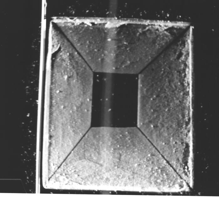
4 OPTICAL PICTURE OF ETCH PIT 20% KOH <100> Si Etch C Page 4

5 PHILLIPS SEM Page 5


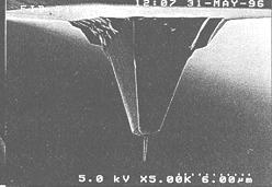
6 SEM PICTURES These SEM pictures show typical profiles of aluminum over steps from the CVC601. Page 6

7 SCANNING TUNNELING MICROSCOPE (STM) Z X Y ~ 100 Å Gap Surface I Piezoelectric Motors Scan Tip in X and Y, Electronics control Z such that the Tunneling Current I is Constant. The Control Voltage for Z is a Measure of Surface Topology Page 7

8 ATOMIC FORCE MICROSCOPE (AFM) Page 8


9 ATOMIC FORCE MICROSCOPE (AFM) Standard Sharp Apex Slender Long Used in Contact mode CD Mode (Conical and Flared) Flared tip able to measure undercut sidewalls Used in non-contact mode Page 9
10 LINEWIDTH MEASUREMENT Calibrate the output device for the microscope for a known size object. Then display unknown device and determine size by comparing the unknown to the known size. A filar eyepiece is an eyepiece with a mechanical dial that moves a hairline across the field of view. The markings on the dial are calibrated by measuring a known size object. Unknown size objects are measured by positioning the hairline on one edge of the object, reading the dial and positioning the hairline on the other side of the object and reading the difference. Then calculating the size knowing the calibration. This technique is limited to objects small enough to fit within the field of view. For larger objects a calibrated traveling stage with a fixed hairline within the eyepiece can be used. Newer systems use CCD camera pixel counting rather than a mechanical eyepiece. Page 10
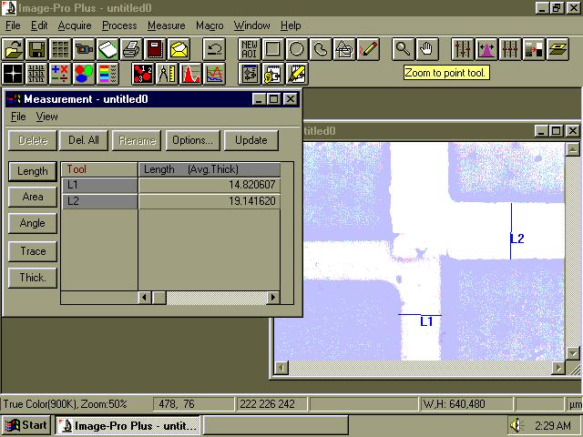
11 LINEWIDTH MEASUREMENT SYSTEM Page 11
12 HEIGHT MEASUREMENT USING OPTICAL MICROSCOPE Dial divisions are inch units equal to 25.4 µm accuracy is about 1/2 division or 12.5 µm, this is good for measuring thickness in the 100 s of microns range Page 12 Focus and height measurement each division is 1 µm

13 HEIGHT MEASUREMENT USING OPTICAL MICROSCOPE Put object on the microscope and obtain an image then place the micrometer under the stage as shown to measure the height change as the focus knob is turned Use the 100 x Objective Lens for smallest depth of focus Focus on top of object and set micrometer dial to zero Focus on bottom of object and read the height on the micrometer dial. Page 13

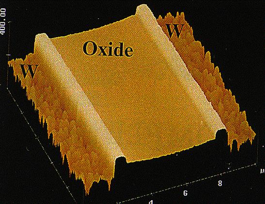
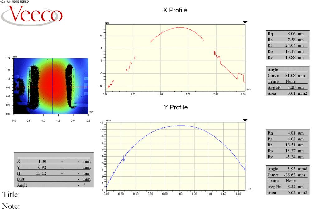
14 OPTICAL TECHNIQUES FOR HEIGHT AND DISPLACEMENT 3D Surface Topography Heights 0.1 nm to 5 mm Resolution 0.1 nm Page 14

15 RIT s VEECO WYCO NT1100 OPTICAL PROFILOMETER Used to measure RMS surface roughness Page 15


16 VEECO DYNAMIC OPTICAL PROFILER Page 16


17 SURFACE ROUGHNESS DATA Bare Silicon Wafer ~5nm RMS Aluminum CVC Å ~15nm RMS Page 17


18 RIT S OTHER WYCO HEIGHT MEASUREMENT TOOL Page 18

19 HEIGHT MEASUREMENT USING OPTICAL MICROSCOPE 500 µm 31 µm 20% KOH 72 C, 10 Hrs. Page 19

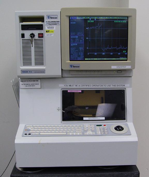
20 TENCORE P2 LONG SCAN PROFILOMETER Page 20

21 STYLUS SURFACE PROFILOMETER 10 0 Readout Film Thickness 1,000 Å < Max < 1,000,000 Å Stylus Film Page 21
22 OXIDE THICKNESS COLOR CHART Thick ness Color Thickness Color 500 Tan 4900 Blue Blue 700 Brown 5000 Blue Green 1000 Dark Violet - Red Violet 5200 Green 1200 Royal Blue 5400 Yellow Green Blue 1500 Light Blue - Metallic Blue 5600 GreenYellow 1700 Metallic - very light Yellow Green 5700 Yel low -"Yel lowish"(at times app ears to b e Lt gray o r matel 2000 LIght Gold or Yellow - Slightly Metallic X other materials 5800 = Light X oxide Orange or 1.45/n Yellow - Pink other material 2200 Gold with slight Yellow Orange 6000 Carnation Pink 2500 Orange - Melon 6300 Violet Red 2700 Red Violet 6800 "Bluish"(appears violet red, Blue Green, look s gray Blueish) 3000 Blue - Violet Blue 7200 Blue Green - Green 3100 Blue Blue 7700 "Yellowish" 3200 Blue - Blue Green 8000 Orange 3400 Light Green 8200 Salmon 3500 Green - Yellow Green 8500 Dull, LIght Red Violet 3600 Yellow Green 8600 Violet 3700 Yellow 8700 Blue Violet 3900 Light Orange 8900 Blue Blue 4100 Carnation Pink 9200 Blue Green 4200 Violet Red 9500 Dull Yellow Green 4400 Red Violet 9700 Yellow - "Yellowish" 4600 Violet 9900 Orange 4700 Blue Violet Carnation Pink Nitride Rochester Institute Thickness of Technology = (Oxide Thickness)(Oxide Index/Nitride Index) Microelectronic Eg. Engineering Yellow Nitride Thickness = (2000)(1.46/2.00) = 1460 Page 22
23 (REFLECTANCE SPECTROMETER) NANOSPEC THICKNESS MEASUREMENT INCIDENT WHITE LIGHT, THE INTENSITY OF THE REFLECTED LIGHT IS MEASURED VS WAVELENGTH 3000 Å OXIDE 7000 Å OXIDE MONOCHROMATOR & DETECTOR λ λ WHITE LIGHT SOURCE WAFER OPTICS Oxide on Silicon ,000 Å Nitride ,000 Neg Resist ,000 Poly on Ox ,000 Neg Resist on Ox Nitride on Oxide Thin Oxide Thin Nitride Polyimide ,000 Positive Resist ,000 Pos Resist on Ox ,000 4,000-30,000 Page 23

24 NANOSPEC FILM THICKNESS MEASUREMENT TOOL Page 24


25 TENCORE SPECROMAP Record: Mean Std Deviation Min Max No of Points Page 25
26 ELLIPSOMETRY LIGHT SOURCE QUARTER WAVE PLATE POLARIZER unpolarized linear polarized SURFACE elliptic linear polarized ANALYZER null FILTER (blocke s out room light) PHOTO DETECTOR The light source is unpolarized, upon traversing the polarizer the light becomes linearly polarized. Turning the polarizer adjusts the azimuth of linearly polarized light with respect to the fast axis of the quarter-wave plate in such a way as to vary the ellipticity of the light incident on the surface. This ellipticity is adjusted until it is just cancelled by the ellipticity introduced by the reflection. The result is again linearly polarized light. The analyzer polarizing prism is rotated until its axis of polarization is perpendicular to the azimuth of the linearly polarized light, creating a null. Thus no light is transmitted to the dedector. The common technique is to fix the quarter-wave plate with fast axis at 45 to the plane of incidence, and to alternately move the polarizer and analyzer, continuously reducing the transmitted light until a null is reached. The relevant light parameters and Ψ are readily calculated from the instrument parameters (P, polarizer angle, Q, quarter-wave plate angle, and A, analyzer angle. Values for film thickness and index of refraction are found. Thickness values that correspond to these parameters repeat with multiples of the light source wavelength so the approximate thickness must be known. Page 26


27 ELLIPSOMETER Rudolph Ellipsometer Variable Angle Spectroscopic Ellipsometer Page 27
 Staining Solution - 1 Vol part HF, 2 Vol part Nitric Acid, 12 Vol part Acetic Acid After mixing drop a penny in solution for about 10 sec. result in a light blue color.")
28 GROOVE and STAIN FIND Xj AFTER PRE DEPOSIT OR DRIVE-IN Groove D M N M N After Stain Xj = (N * M) / D (at RIT D=1.532 inch) Staining Solution - 1 Vol part HF, 2 Vol part Nitric Acid, 12 Vol part Acetic Acid After mixing drop a penny in solution for about 10 sec. result in a light blue color. Safety Stain - (does not have HF) is available from Philtec Instrument Co. Philadelphia, PA , (215) , Signatone makes groove tool and wheels, (408) Page 28
 / D = (0.025 * 0.003)/1.532 inch) = 0.0000472 inch = 1.")
29 TRAVELING STAGE MICROSCOPE Example: If M=.003 inches and N=0.025 inches, find xj. Xj = (N * M) / D = (0.025 * 0.003)/1.532 inch) = inch = 1.20 µm Poly on Oxide on Silicon (no stain) Page 29
30 DEPTH WITH TRAVELING STAGE MICROSCOPE 100µm KOH etches silicon along the (111) crystal plane giving a 53 angle. Example: the traveling stage microscope is used to measure the 100 µm distance shown. The depth is calculated. Tan 53 = depth/100µm depth = 133 µm Page 30

31 ETCH STEPS IN OXIDE TO FIND ETCH RATE 5000 Å BARE SILICON Page 31
32 STEP ETCH APPARATUS BUFFERED HF Lower 1/4 inch every 45 seconds Page 32
33 GROOVE AND STAIN AND 4PTPROBE FIND SHEET RESISTANCE AND RESISTIVITY FOR A DIFFUSED LAYER Groove After Stain Xj = (N * M) / D D M N Xj S I M V N 4PT PROBE Xj Rhos = V / I * π / ln 2 = V/I ohms/square Rho = Rhos Xj ohm-cm Page 33
34 FOUR POINT PROBE - RESISTIVITY FOUR POINT PROBE I V S = probe spacing W = wafer thickness Rho = π/ln2 x W x V / I ohm-cm if S<<W and S<<Wafer Diameter Page 34


35 4 PT PROBE METAL THICKNESS MEASUREMENTS Rho=Rhos x t CDE Resistivity Mapper Tool gives Rho or Rhos depending on recipe used, automatically adjusts correction factors for wafer thickness t = Rho/Rhos Page 35

36 SPUTTERED ALUMINUM THICKNESS UNIFORMITY CVC601 Ave = 6.03K Min = 4.73K Max = 7.68K Non Uniformity = 23.78% Page 36


37 STRESS IN POLY AND NITRIDE FILMS Test Structures for Measuring stress in Silicon Nitride Films Page 37
38 LOW STRESS SILICON RICH Si3N4 ADE Measured stress for various Ammonia: Dichlorosilane Flow Ratios Flow Stress x E 9 dynes/cm2 10: : : Stress: σ = (E/(6(1-v)))*(D 2 /(rt)) 1: where E is Youngs modulus, 1: * v is Poissons ratio, 1:5 +3 D and t are substrate and film thickness 1:10 0 r is radius of curvature (- for tensile) *standard recipe T.H Wu, Stress in PSG and Nitride Films as Related to Film Properties and Annealing, Solid State Technology, p 65-71,May dyne/cm 2 = 1 newton/m 2 = 1 Pascal Page 38
39 REFERENCES 1. Mechanics of Materials, by Ferdinand P. Beer, E. Russell Johnston, Jr., McGraw-Hill Book Co.1981, ISBN Etch Rates for Micromachining Processing, Journal of Microelectromechanical Systems, Vol.5, No.4, December Crystalline Semiconductor Micromachine, Seidel, Proceedings of the 4th Int. Conf. on Solid State Sensors and Actuators 1987, p Optical height measurements, Page 39
40 HOMEWORK - MEASUREMENTS FOR MEMS 1. Derive the equation used in the groove and stain technique for measuring junction depth. 2. Describe 5 ways to estimate/measure the thickness of a polysilicon film that you deposit. 3. How does the nanospec work? What is the difference in its operation for thin oxides compared to thicker oxides? Why? Page 40
Photoresist Coat, Expose and Develop Laboratory Dr. Lynn Fuller
 ROCHESTER INSTITUTE OF TECHNOLOGY MICROELECTRONIC ENGINEERING Photoresist Coat, Expose and Develop Laboratory Dr. Lynn Fuller Webpage: http://www.rit.edu/lffeee 82 Lomb Memorial Drive Rochester, NY 14623-5604
Piezoresistance in Silicon. Dr. Lynn Fuller Webpage:
 ROCHESTER INSTITUTE OF TECHNOLOGY MICROELECTRONIC ENGINEERING Piezoresistance in Silicon Webpage: http://people.rit.edu/lffeee 82 Lomb Memorial Drive Rochester, NY 14623-5604 Tel (585) 475-2035 Email:
Rapid Thermal Processing (RTP) Dr. Lynn Fuller
 Dr. Lynn Fuller") ROCHESTER INSTITUTE OF TECHNOLOGY MICROELECTRONIC ENGINEERING Rapid Thermal Processing (RTP) Dr. Lynn Fuller Webpage: http://people.rit.edu/lffeee 82 Lomb Memorial Drive Rochester, NY 14623-5604 Tel (585)
ROCHESTER INSTITUTE OF TECHNOLOGY MICROELECTRONIC ENGINEERING Rapid Thermal Processing (RTP) Dr. Lynn Fuller Webpage: http://people.rit.edu/lffeee 82 Lomb Memorial Drive Rochester, NY 14623-5604 Tel (585)
Isolation Technology. Dr. Lynn Fuller
 ROCHESTER INSTITUTE OF TECHNOLOGY MICROELECTRONIC ENGINEERING Isolation Technology Dr. Lynn Fuller Motorola Professor 82 Lomb Memorial Drive Rochester, NY 14623-5604 Tel (585) 475-2035 Fax (585) 475-5041
LAM 490 Etch Recipes. Dr. Lynn Fuller
 ROCHESTER INSTITUTE OF TECHNOLOGY MICROELECTRONIC ENGINEERING LAM 490 Etch Recipes Dr. Lynn Fuller Professor, Webpage: http://people.rit.edu/lffeee 82 Lomb Memorial Drive Rochester, NY 14623-5604 Tel (585)
Surface micromachining and Process flow part 1
 Surface micromachining and Process flow part 1 Identify the basic steps of a generic surface micromachining process Identify the critical requirements needed to create a MEMS using surface micromachining
ME 141B: The MEMS Class Introduction to MEMS and MEMS Design. Sumita Pennathur UCSB
 ME 141B: The MEMS Class Introduction to MEMS and MEMS Design Sumita Pennathur UCSB Outline today Introduction to thin films Oxidation Deal-grove model CVD Epitaxy Electrodeposition 10/6/10 2/45 Creating
Drytech Quad Etch Recipes Dr. Lynn Fuller Mike Aquilino Microelectronic Engineering
 ROCHESTER INSTITUTE OF TECHNOLOGY MICROELECTRONIC ENGINEERING Drytech Quad Etch Recipes Dr. Lynn Fuller Mike Aquilino 82 Lomb Memorial Drive Rochester, NY 14623-5604 Tel (585) 475-2035 Fax (585) 475-5041
Microelectromechanical Systems (MEMs) Materials for MEMs
 Materials for MEMs") ROCHESTER INSTITUTE OF TEHNOLOGY MICROELECTRONIC ENGINEERING Microelectromechanical Systems (MEMs) Materials for MEMs Dr. Lynn Fuller Webpage: http://people.rit.edu/lffeee 82 Lomb Memorial Drive Rochester,
ROCHESTER INSTITUTE OF TEHNOLOGY MICROELECTRONIC ENGINEERING Microelectromechanical Systems (MEMs) Materials for MEMs Dr. Lynn Fuller Webpage: http://people.rit.edu/lffeee 82 Lomb Memorial Drive Rochester,
Microstructures using RF sputtered PSG film as a sacrificial layer in surface micromachining
 Sādhanā Vol. 34, Part 4, August 2009, pp. 557 562. Printed in India Microstructures using RF sputtered PSG film as a sacrificial layer in surface micromachining VIVEKANAND BHATT 1,, SUDHIR CHANDRA 1 and
Optical characterization of an amorphoushydrogenated carbon film and its application in phase modulated diffractive optical elements
 Optical characterization of an amorphoushydrogenated carbon film and its application in phase modulated diffractive optical elements G. A. Cirino a, P. Verdonck a, R. D. Mansano a, L. G. Neto b a LSI-PEE-EPUSP
JSM-7800F Field Emission Scanning Electron Microscope
 JSM-7800F catalogue JSM-7800F Field Emission Scanning Electron Microscope We provide high performance The Ultimate Research Tool for Multi-Disciplinary Research Institutions Extreme resolution The super
Lab #2 Wafer Cleaning (RCA cleaning)
") Lab #2 Wafer Cleaning (RCA cleaning) RCA Cleaning System Used: Wet Bench 1, Bay1, Nanofabrication Center Chemicals Used: H 2 O : NH 4 OH : H 2 O 2 (5 : 1 : 1) H 2 O : HF (10 : 1) H 2 O : HCl : H 2 O 2
Lab #2 Wafer Cleaning (RCA cleaning) RCA Cleaning System Used: Wet Bench 1, Bay1, Nanofabrication Center Chemicals Used: H 2 O : NH 4 OH : H 2 O 2 (5 : 1 : 1) H 2 O : HF (10 : 1) H 2 O : HCl : H 2 O 2
Oxide Growth. 1. Introduction
 Oxide Growth 1. Introduction Development of high-quality silicon dioxide (SiO2) has helped to establish the dominance of silicon in the production of commercial integrated circuits. Among all the various
Thin Nitride Measurement Example
 Thin Nitride Measurement Example GOAL: Get the most information from your data and analyze it properly to make the right decisions! Look at the data in multiple ways to understand your process better.
HOMEWORK 4 and 5. March 15, Homework is due on Monday March 30, 2009 in Class. Answer the following questions from the Course Textbook:
 HOMEWORK 4 and 5 March 15, 2009 Homework is due on Monday March 30, 2009 in Class. Chapter 7 Answer the following questions from the Course Textbook: 7.2, 7.3, 7.4, 7.5, 7.6*, 7.7, 7.9*, 7.10*, 7.16, 7.17*,
Advanced CMOS Process Technology Part 3 Dr. Lynn Fuller
 MICROELECTRONIC ENGINEERING ROCHESTER INSTITUTE OF TECHNOLOGY Part 3 Dr. Lynn Fuller Webpage: http://people.rit.edu/lffeee Electrical and Microelectronic Engineering Rochester Institute of Technology 82
Poly-SiGe MEMS actuators for adaptive optics
 Poly-SiGe MEMS actuators for adaptive optics Blake C.-Y. Lin a,b, Tsu-Jae King a, and Richard S. Muller a,b a Department of Electrical Engineering and Computer Sciences, b Berkeley Sensor and Actuator
Lecture 5. SOI Micromachining. SOI MUMPs. SOI Micromachining. Silicon-on-Insulator Microstructures. Agenda:
 EEL6935 Advanced MEMS (Spring 2005) Instructor: Dr. Huikai Xie SOI Micromachining Agenda: SOI Micromachining SOI MUMPs Multi-level structures Lecture 5 Silicon-on-Insulator Microstructures Single-crystal
R&D ACTIVITIES AT ASSCP-BHEL,GURGAON IN SOLAR PV. DST-EPSRC Workshop on Solar Energy Research
 R&D ACTIVITIES AT -BHEL,GURGAON IN SOLAR PV at the DST-EPSRC Workshop on Solar Energy Research (22 nd 23 rd April, 2009) by Dr.R.K. Bhogra, Addl. General Manager & Head Email: cpdrkb@bhel.co.in Dr.A.K.
Chapter 2. Density 2.65 g/cm 3 Melting point Young s modulus Tensile strength Thermal conductivity Dielectric constant 3.
 Chapter 2 Thin Film Materials Thin films of Silicon dioxide, Silicon nitride and Polysilicon have been utilized in the fabrication of absolute micro pressure sensor. These materials are studied and discussed
Slow DNA Transport through Nanopores in Hafnium Oxide Membranes
 Slow DNA Transport through Nanopores in Hafnium Oxide Membranes Joseph Larkin, Robert Henley, David C. Bell, Tzahi Cohen-Karni, # Jacob K. Rosenstein, and Meni Wanunu * Departments of Physics and Chemistry/Chemical
The growth of patterned ceramic thin films from polymer precursor solutions Göbel, Ole
 University of Groningen The growth of patterned ceramic thin films from polymer precursor solutions Göbel, Ole IMPORTANT NOTE: You are advised to consult the publisher's version (publisher's PDF) if you
Ion Implantation Most modern devices doped using ion implanters Ionize gas sources (single +, 2+ or 3+ ionization) Accelerate dopant ions to very
 Accelerate dopant ions to very") Ion Implantation Most modern devices doped using ion implanters Ionize gas sources (single +, 2+ or 3+ ionization) Accelerate dopant ions to very high voltages (10-600 KeV) Use analyzer to selection charge/mass
Ion Implantation Most modern devices doped using ion implanters Ionize gas sources (single +, 2+ or 3+ ionization) Accelerate dopant ions to very high voltages (10-600 KeV) Use analyzer to selection charge/mass
Improvement of Laser Fuse Processing of Fine Pitch Link Structures for Advanced Memory Designs
 Improvement of Laser Fuse Processing of Fine Pitch Link Structures for Advanced Memory Designs Joohan Lee, Joseph J. Griffiths, and James Cordingley GSI Group Inc. 60 Fordham Rd. Wilmington, MA 01887 jlee@gsig.com
2015 EE410-LOCOS 0.5µm Poly CMOS Process Run Card Lot ID:
 STEP 0.00 - PHOTOMASK #0- ZERO LEVEL MARKS Starting materials is n-type silicon (5-10 ohm-cm). Add four test wafers labeled T1-T4. T1 and T2 will travel with the device wafers and get all of the processing
Evaluation of Mechanical Properties of Hard Coatings
 Evaluation of Mechanical Properties of Hard Coatings Comprehensive mechanical testing of two coated metal samples was performed on the UNMT- 1. The tests clearly distinguished brittle and ductile samples,
Precision Optical Engineering
 Precision Optical Engineering Products: Prisms Windows Mirrors Flats and Master angles Sight Glasses Key Features: Prisms (Contacted, Cemented, AR coated, Mounted) Windows (Flat, wedged, curved, drilled,
Overview of CMP for TSV Applications. Robert L. Rhoades, Ph.D. Presentation for AVS Joint Meeting June 2013 San Jose, CA
 Overview of CMP for TSV Applications Robert L. Rhoades, Ph.D. Presentation for AVS Joint Meeting June 2013 San Jose, CA Outline TSV s and the Role of CMP TSV Pattern and Fill TSV Reveal (non-selective)
At wavelength characterization of EUV and soft X-ray gratings
 At wavelength characterization of EUV and soft X-ray gratings F. Scholze, A, Haase, C. Laubis, V. Soltwisch, J. Wernecke, M. Krumrey Physikalisch-Technische Bundesanstalt, Abbestraße 2-12, 10587 Berlin,
Growth and Doping of SiC-Thin Films on Low-Stress, Amorphous Si 3 N 4 /Si Substrates for Robust Microelectromechanical Systems Applications
 Journal of ELECTRONIC MATERIALS, Vol. 31, No. 5, 2002 Special Issue Paper Growth and Doping of SiC-Thin Films on Low-Stress, Amorphous Si 3 N 4 /Si Substrates for Robust Microelectromechanical Systems
National Semiconductor LM2672 Simple Switcher Voltage Regulator
 Construction Analysis National Semiconductor LM2672 Simple Switcher Voltage Regulator Report Number: SCA 9712-570 Global Semiconductor Industry the Serving Since 1964 17350 N. Hartford Drive Scottsdale,
3.155J / 6.152J Micro/Nano Processing Technology TAKE-HOME QUIZ FALL TERM 2005
 3.155J / 6.152J Micro/Nano Processing Technology TAKE-HOME QUIZ FALL TERM 2005 1) This is an open book, take-home quiz. You are not to consult with other class members or anyone else. You may discuss the
Thin Films: Sputtering Systems (Jaeger Ch 6 & Ruska Ch 7,) Sputtering: gas plasma transfers atoms from target to substrate Can deposit any material
 Sputtering: gas plasma transfers atoms from target to substrate Can deposit any material") Thin Films: Sputtering Systems (Jaeger Ch 6 & Ruska Ch 7,) Sputtering: gas plasma transfers atoms from target to substrate Can deposit any material on any substrate (in principal) Start with pumping down
Thin Films: Sputtering Systems (Jaeger Ch 6 & Ruska Ch 7,) Sputtering: gas plasma transfers atoms from target to substrate Can deposit any material on any substrate (in principal) Start with pumping down
Precision Electroforming in High-Strength NiColoy
 Taking the Stress out of Electroforming www.nicoform.com Precision Electroforming in High-Strength NiColoy Copyright 2007 NiCoForm, Inc. (Rochester, NY) Electroforming What is it? What is it good for?
Surface Micromachining
 Surface Micromachining Outline Introduction Material often used in surface micromachining Material selection criteria in surface micromachining Case study: Fabrication of electrostatic motor Major issues
Section 4: Thermal Oxidation. Jaeger Chapter 3. EE143 - Ali Javey
 Section 4: Thermal Oxidation Jaeger Chapter 3 Properties of O Thermal O is amorphous. Weight Density =.0 gm/cm 3 Molecular Density =.3E molecules/cm 3 O Crystalline O [Quartz] =.65 gm/cm 3 (1) Excellent
Measurement of thickness of native silicon dioxide with a scanning electron microscope
 Measurement of thickness of native silicon dioxide with a scanning electron microscope V. P. Gavrilenko* a, Yu. A. Novikov b, A. V. Rakov b, P. A. Todua a a Center for Surface and Vacuum Research, 40 Novatorov
MEMS prototyping using RF sputtered films
 Indian Journal of Pure & Applied Physics Vol. 45, April 2007, pp. 326-331 MEMS prototyping using RF sputtered films Sudhir Chandra, Vivekanand Bhatt, Ravindra Singh, Preeti Sharma & Prem Pal* Centre for
DETERMINATION OF DEGREE OF CARBONIZATION IN COKES BY IMAGE ANALYSIS. Abstract. Background
 DETERMINATION OF DEGREE OF CARBONIZATION IN COKES BY IMAGE ANALYSIS Stein Rørvik, SINTEF Materials and Chemistry, Sem Sælands vei 12, N-7465 Trondheim, Norway Arne Petter Ratvik, SINTEF Materials and Chemistry,
LAM4600 Plasma Etch Tool Recipes Dr. Lynn Fuller Webpage:
 ROCHESTER INSTITUTE OF TECHNOLOGY MICROELECTRONIC ENGINEERING LAM4600 Plasma Etch Tool Recipes Webpage: http://people.rit.edu/lffeee 82 Lomb Memorial Drive Rochester, NY 14623-5604 Tel (585) 475-2035 Email:
Surface MEMS Fabrication Blog Dr. Lynn Fuller, Adam Wardas Webpage:
 ROCHESTER INSTITUTE OF TECHNOLOGY MICROELECTRONIC ENGINEERING Surface MEMS Fabrication Blog Dr. Lynn Fuller, Adam Wardas Webpage: http://people.rit.edu/lffeee 82 Lomb Memorial Drive Rochester, NY 14623-5604
EE C245 ME C218 Introduction to MEMS Design Fall 2011
 Lecture Outline EE C245 ME C218 Introduction to MEMS Design Fall 2011 Prof. Clark T.-C. Nguyen Dept. of Electrical Engineering & Computer Sciences University of California at Berkeley Berkeley, CA 94720
4. Thermal Oxidation. a) Equipment Atmospheric Furnace
 Equipment Atmospheric Furnace") 4. Thermal Oxidation a) Equipment Atmospheric Furnace Oxidation requires precise control of: temperature, T ambient gas, G time spent at any given T & G, t Vito Logiudice 34 4. Thermal Oxidation b) Mechanism
4. Thermal Oxidation a) Equipment Atmospheric Furnace Oxidation requires precise control of: temperature, T ambient gas, G time spent at any given T & G, t Vito Logiudice 34 4. Thermal Oxidation b) Mechanism
Sketch the light paths from object to image in a single lens system in following situations.
 Solutions o Chapter I 1.1. There are three rules governing light path or a simple lens: 1) light ray passing through the center o a lens is not deviated. ) Light ray parallel with optic axis will pass
EXCIMER LASER ANNEALING FOR LOW- TEMPERATURE POLYSILICON THIN FILM TRANSISTOR FABRICATION ON PLASTIC SUBSTRATES
 EXCIMER LASER ANNEALING FOR LOW- TEMPERATURE POLYSILICON THIN FILM TRANSISTOR FABRICATION ON PLASTIC SUBSTRATES G. Fortunato, A. Pecora, L. Maiolo, M. Cuscunà, D. Simeone, A. Minotti, and L. Mariucci CNR-IMM,
Silver Diffusion Bonding and Layer Transfer of Lithium Niobate to Silicon
 Chapter 5 Silver Diffusion Bonding and Layer Transfer of Lithium Niobate to Silicon 5.1 Introduction In this chapter, we discuss a method of metallic bonding between two deposited silver layers. A diffusion
Materials Characterization
 Materials Characterization C. R. Abernathy, B. Gila, K. Jones Cathodoluminescence (CL) system FEI Nova NanoSEM (FEG source) with: EDAX Apollo silicon drift detector (TE cooled) Gatan MonoCL3+ FEI SEM arrived
Micro-Electro-Mechanical Systems (MEMS) Fabrication. Special Process Modules for MEMS. Principle of Sensing and Actuation
 Fabrication. Special Process Modules for MEMS. Principle of Sensing and Actuation") Micro-Electro-Mechanical Systems (MEMS) Fabrication Fabrication Considerations Stress-Strain, Thin-film Stress, Stiction Special Process Modules for MEMS Bonding, Cavity Sealing, Deep RIE, Spatial forming
Micro-Electro-Mechanical Systems (MEMS) Fabrication Fabrication Considerations Stress-Strain, Thin-film Stress, Stiction Special Process Modules for MEMS Bonding, Cavity Sealing, Deep RIE, Spatial forming
Transmission Electron Microscopy (TEM) Prof.Dr.Figen KAYA
 Prof.Dr.Figen KAYA") Transmission Electron Microscopy (TEM) Prof.Dr.Figen KAYA Transmission Electron Microscope A transmission electron microscope, similar to a transmission light microscope, has the following components along
Transmission Electron Microscopy (TEM) Prof.Dr.Figen KAYA Transmission Electron Microscope A transmission electron microscope, similar to a transmission light microscope, has the following components along
Process Flow in Cross Sections
 Process Flow in Cross Sections Process (simplified) 0. Clean wafer in nasty acids (HF, HNO 3, H 2 SO 4,...) --> wear gloves! 1. Grow 500 nm of SiO 2 (by putting the wafer in a furnace with O 2 2. Coat
EDGE CHIPPING RESISTANCE USING MACROINDENTATION TESTING
 EDGE CHIPPING RESISTANCE USING MACROINDENTATION TESTING Prepared by Ali Mansouri 6 Morgan, Ste156, Irvine CA 92618 P: 949.461.9292 F: 949.461.9232 nanovea.com Today's standard for tomorrow's materials.
Measurement of Residual Stress by X-ray Diffraction
 Measurement of Residual Stress by X-ray Diffraction C-563 Overview Definitions Origin Methods of determination of residual stresses Method of X-ray diffraction (details) References End Stress and Strain
NANO SCRATCH TESTING OF THIN FILM ON GLASS SUBSTRATE
 NANO SCRATCH TESTING OF THIN FILM ON GLASS SUBSTRATE Prepared by Jesse Angle 6 Morgan, Ste156, Irvine CA 92618 P: 949.461.9292 F: 949.461.9232 nanovea.com Today's standard for tomorrow's materials. 2010
Thin Films: Sputtering Systems (Jaeger Ch 6 & Ruska Ch 7,) Can deposit any material on any substrate (in principal) Start with pumping down to high
 Can deposit any material on any substrate (in principal) Start with pumping down to high") Thin Films: Sputtering Systems (Jaeger Ch 6 & Ruska Ch 7,) Can deposit any material on any substrate (in principal) Start with pumping down to high vacuum ~10-7 torr Removes residual gases eg oxygen from
Thin Films: Sputtering Systems (Jaeger Ch 6 & Ruska Ch 7,) Can deposit any material on any substrate (in principal) Start with pumping down to high vacuum ~10-7 torr Removes residual gases eg oxygen from
Laser Micromachining of Bulk Substrates and Thin Films Celine Bansal
 Laser Micromachining of Bulk Substrates and Thin Films Celine Bansal Oxford Lasers Ltd Moorbrook Park Didcot, Oxfordshire, OX11 7HP Tel: +44 (0) 1235 810088 www.oxfordlasers.com Outline Oxford Lasers Importance
Calibration technique for MEMS membrane type strain sensors
 Calibration technique for MEMS membrane type strain sensors Li Cao a, Tae Song Kim b, Jia Zhou a, Susan C. Mantell a *, and Dennis L. Polla b a Dept. of Mechanical Engineering, University of Minnesota,
PARAMETER EFFECTS FOR THE GROWTH OF THIN POROUS ANODIC ALUMINUM OXIDES
 10.1149/1.2794473, The Electrochemical Society PARAMETER EFFECTS FOR THE GROWTH OF THIN POROUS ANODIC ALUMINUM OXIDES S. Yim a, C. Bonhôte b, J. Lille b, and T. Wu b a Dept. of Chem. and Mat. Engr., San
Proceedings Post Fabrication Processing of Foundry MEMS Structures Exhibiting Large, Out-of-Plane Deflections
 Proceedings Post Fabrication Processing of Foundry MEMS Structures Exhibiting Large, Out-of-Plane Deflections LaVern Starman 1, *, John Walton 1, Harris Hall 1 and Robert Lake 2 1 Sensors Directorate,
Plasma-Enhanced Chemical Vapor Deposition
 Plasma-Enhanced Chemical Vapor Deposition Steven Glenn July 8, 2009 Thin Films Lab 4 ABSTRACT The objective of this lab was to explore lab and the Applied Materials P5000 from a different point of view.
Morphology of Thin Aluminum Film Grown by DC Magnetron Sputtering onto SiO 2 on Si(100) Substrate
 Substrate") Morphology of Thin Aluminum Film Grown by DC Magnetron Sputtering onto SiO 2 on Si(1) Substrate Fan Wu Microelectronics Center, Medtronic Inc., Tempe, AZ 85261 James E. Morris Department of Electrical
Morphology of Thin Aluminum Film Grown by DC Magnetron Sputtering onto SiO 2 on Si(1) Substrate Fan Wu Microelectronics Center, Medtronic Inc., Tempe, AZ 85261 James E. Morris Department of Electrical
Evaluation of length scale effects for micro and nano-sized cantilevered structures
 University of Wollongong Research Online University of Wollongong Thesis Collection 1954-2016 University of Wollongong Thesis Collections 2010 Evaluation of length scale effects for micro and nano-sized
Transmission Kikuchi Diffraction in the Scanning Electron Microscope
 Transmission Kikuchi Diffraction in the Scanning Electron Microscope Robert Keller, Roy Geiss, Katherine Rice National Institute of Standards and Technology Nanoscale Reliability Group Boulder, Colorado
Sputtered Zinc Oxide Films for Silicon Thin Film Solar Cells: Material Properties and Surface Texture
 Poster FVS Workshop 2002 Sputtered Zinc Oxide Films for Silicon Thin Film Solar Cells: Material Properties and Surface Texture Texture etching of sputtered ZnO:Al films has opened up a variety of possibilities
Lecture 19 Microfabrication 4/1/03 Prof. Andy Neureuther
 EECS 40 Spring 2003 Lecture 19 Microfabrication 4/1/03 Prof. ndy Neureuther How are Integrated Circuits made? Silicon wafers Oxide formation by growth or deposition Other films Pattern transfer by lithography
RF sputtering: A viable tool for MEMS fabrication
 Sādhanā Vol. 34, Part 4, August 2009, pp. 543 556. Printed in India RF sputtering: A viable tool for MEMS fabrication SUDHIR CHANDRA, VIVEKANAND BHATT and RAVINDRA SINGH Centre for Applied Research in
Specimen Preparation Technique for a Microstructure Analysis Using the Focused Ion Beam Process
 Specimen Preparation Technique for a Microstructure Analysis Using the Focused Ion Beam Process by Kozue Yabusaki * and Hirokazu Sasaki * In recent years the FIB technique has been widely used for specimen
SUMMiT V Five Level Surface Micromachining Technology Design Manual
 SUMMiT V Five Level Surface Micromachining Technology Design Manual Version 1.3 09/22/2005 MEMS Devices and Reliability Physics Department Microelectronics Development Laboratory Sandia National Laboratories
Characteristics of machined surface controlled by cutting tools and conditions in machining of brittle material
 Characteristics of machined surface controlled by cutting tools and conditions in machining of brittle material Yong-Woo KIM 1, Soo-Chang CHOI 1, Jeung-Woo PARK 2, Deug-Woo LEE 3 1. Department of Nano
Resolving lateral and vertical structures by ellipsometry using wavelength range scan
 *Manuscript Click here to view linked References Resolving lateral and vertical structures by ellipsometry using wavelength range scan P. Petrik a,b, E. Agocs a,b, J. Volk a, I. Lukacs a, B. Fodor a,c,
ALD systems and SENTECH Instruments GmbH
 ALD systems and processes @ SENTECH Instruments GmbH H. Gargouri, F. Naumann, R. Rudolph and M. Arens SENTECH Instruments GmbH, Berlin www.sentech.de 1 2 Agenda 1. Company Introduction 2. SENTECH-ALD-Systems
Highly Durable Fuel Cell Electrode Based on Ionomer Dispersed in Glycerol
 Electronic Supplementary Material (ESI) for Physical Chemistry Chemical Physics. This journal is The Royal Society of Chemistry 214 Electronic Supplementary Information Highly Durable Fuel Cell Electrode
Coatings. Ion Assisted Deposition (IAD) process Advance Plasma Source (APS) plasma-ion assisted Deposition. Coatings on Optical Fibers
 process Advance Plasma Source (APS) plasma-ion assisted Deposition. Coatings on Optical Fibers") Anti-Reflection Custom Ion Assisted Deposition (IAD) process Advance Plasma Source (APS) plasma-ion assisted Deposition Anti-Reflection on Optical Fibers OptoSigma supplies a wide selection of optical
Anti-Reflection Custom Ion Assisted Deposition (IAD) process Advance Plasma Source (APS) plasma-ion assisted Deposition Anti-Reflection on Optical Fibers OptoSigma supplies a wide selection of optical
Mater. Res. Soc. Symp. Proc. Vol Materials Research Society
 Mater. Res. Soc. Symp. Proc. Vol. 940 2006 Materials Research Society 0940-P13-12 A Novel Fabrication Technique for Developing Metal Nanodroplet Arrays Christopher Edgar, Chad Johns, and M. Saif Islam
Modification of Glass by FS Laser for Optical/Memory Applications
 Modification of Glass by FS Laser for Optical/Memory Applications Kazuyuki Hirao and Kiyotaka Miura Department of Material Chemistry Kyoto University International Workshop on Scientific Challenges of
Optical Coatings. Photonics 4 Luxury Coatings , Genève. Dr. Andreas Bächli Head of Optical Coatings at RhySearch, Buchs (SG)
") Optical Coatings Photonics 4 Luxury Coatings 21.06.2017, Genève Dr. Andreas Bächli Head of Optical Coatings at RhySearch, Buchs (SG) RhySearch The Research- and Innovation Center in the Rhine Valley RhySearch
Optical Coatings Photonics 4 Luxury Coatings 21.06.2017, Genève Dr. Andreas Bächli Head of Optical Coatings at RhySearch, Buchs (SG) RhySearch The Research- and Innovation Center in the Rhine Valley RhySearch
FABRICATION PROCESSES FOR MAGNETIC MICROACTUATORS WITH POLYSILICON FLEXURES. Jack W. Judy and Richard S. Muller
 FABRICATION PROCESSES FOR MAGNETIC MICROACTUATORS WITH POLYSILICON FLEXURES Jack W. Judy and Richard S. Muller Berkeley Sensor & Actuator Center (BSAC) Department of EECS, University of California, Berkeley,
THIN FILM THICKNESS MEASUREMENT FOR EVALUATION OF RESIDUAL LAYER OF NANO-IMPRINT LITHOGRAPHY USING NEAR-FIELD OPTICS
 9 th INTERNATIONAL SYMPOSIUM ON MEASUREMENT AND QUALITY CONTROL (9 th ISMQC) November 21 24, 27, IIT Madras THIN FILM THICKNESS MEASUREMENT FOR EVALUATION OF RESIDUAL LAYER OF NANO-IMPRINT LITHOGRAPHY
Analysis of optical properties of solar energy materials
 Analysis of optical properties of solar energy materials Comices Energie solaire - Namur - 23/04/2012 Michel Voué Physique des Matériaux et Optique Centre de Recherche en Physique des Matériaux Université
Quiz on Monday covering: -symmetry operations -notations of axes, vectors, and face notation -Miller indices
 OTHER ANNOUNCEMENTS Quiz on Monday covering: -symmetry operations -notations of axes, vectors, and face notation -Miller indices 2 nd Draft of References due Monday Field Trip Saturday 10/4 and Sunday
MICROFABRICATION OF OPTICALLY ACTIVE InO X MICROSTRUCTURES BY ULTRASHORT LASER PULSES
 Journal of Optoelectronics and Advanced Materials Vol. 4, No. 3, September 2002, p. 809-812 MICROFABRICATION OF OPTICALLY ACTIVE InO X MICROSTRUCTURES BY ULTRASHORT LASER PULSES Foundation for Research
Nanoscale Imaging, Material Removal and Deposition for Fabrication of Cutting-edge Semiconductor Devices
 Hitachi Review Vol. 65 (2016), No. 7 233 Featured Articles Nanoscale Imaging, Material Removal and Deposition for Fabrication of Cutting-edge Semiconductor Devices Ion-beam-based Photomask Defect Repair
200mm Next Generation MEMS Technology update. Florent Ducrot
 200mm Next Generation MEMS Technology update Florent Ducrot The Most Exciting Industries on Earth Semiconductor Display Solar 20,000,000x reduction in COST PER TRANSISTOR in 30 years 1 20x reduction in
300mm Wafer Stain Formation by Spin Etching
 10.1149/1.2980313 The Electrochemical Society 300mm Wafer Stain Formation by Spin Etching K. Sato a, S. Mashimoto a, and M. Watanabe a a Process Development, SEZ Japan, Inc., Hongo, Bunkyo-ku 1130033,
Scale Effects in Freestanding Thin Metal Films for RF MEMS Applications
 Eindhoven University of Technology Department of Mechanical Engineering Materials Technology Scale Effects in Freestanding Thin Metal Films for RF MEMS Applications Student: Zlata Jelacic Supervisors:
Figure 2.3 (cont., p. 60) (e) Block diagram of Pentium 4 processor with 42 million transistors (2000). [Courtesy Intel Corporation.
 (e) Block diagram of Pentium 4 processor with 42 million transistors (2000). [Courtesy Intel Corporation.") Figure 2.1 (p. 58) Basic fabrication steps in the silicon planar process: (a) oxide formation, (b) selective oxide removal, (c) deposition of dopant atoms on wafer, (d) diffusion of dopant atoms into exposed
Figure 2.1 (p. 58) Basic fabrication steps in the silicon planar process: (a) oxide formation, (b) selective oxide removal, (c) deposition of dopant atoms on wafer, (d) diffusion of dopant atoms into exposed
Dallas Semicoductor DS80C320 Microcontroller
 Construction Analysis Dallas Semicoductor DS80C320 Microcontroller Report Number: SCA 9702-525 Global Semiconductor Industry the Serving Since 1964 15022 N. 75th Street Scottsdale, AZ 85260-2476 Phone:
Intel Pentium Processor W/MMX
 Construction Analysis Intel Pentium Processor W/MMX Report Number: SCA 9706-540 Global Semiconductor Industry the Serving Since 1964 15022 N. 75th Street Scottsdale, AZ 85260-2476 Phone: 602-998-9780 Fax:
Lecture 10: MultiUser MEMS Process (MUMPS)
") MEMS: Fabrication Lecture 10: MultiUser MEMS Process (MUMPS) Prasanna S. Gandhi Assistant Professor, Department of Mechanical Engineering, Indian Institute of Technology, Bombay, 1 Recap Various VLSI based
MEMS: Fabrication Lecture 10: MultiUser MEMS Process (MUMPS) Prasanna S. Gandhi Assistant Professor, Department of Mechanical Engineering, Indian Institute of Technology, Bombay, 1 Recap Various VLSI based
Motorola PC603R Microprocessor
 Construction Analysis Motorola PC603R Microprocessor Report Number: SCA 9709-551 Global Semiconductor Industry the Serving Since 1964 17350 N. Hartford Drive Scottsdale, AZ 85255 Phone: 602-515-9780 Fax:
Chapter 1 Electronic and Photonic Materials Liquid Crystal Display. Photonic Materials - Liquid Crystal Display
 Photonic Materials - Liquid Crystal Display 1 2 Liquid Crystal Liquid crystals are organic compounds that flow like a liquid while maintaining a long range orderliness of a solid. The molecules of liquid
16.2 Scanning Infrared Spectrometers
 16.2 Scanning Infrared Spectrometers it's difficult to find materials transparent in the infrared water vapor and atmospheric CO 2 can cause problems there are three common sources high diffraction orders
Modeling of Local Oxidation Processes
 Introduction Isolation Processes in the VLSI Technology Main Aspects of LOCOS simulation Athena Oxidation Models Several Examples of LOCOS structures Calibration of LOCOS effects using VWF Field Oxide
Development of nano-roughness calibration standards
 Home Search Collections Journals About Contact us My IOPscience Development of nano-roughness calibration standards This article has been downloaded from IOPscience. Please scroll down to see the full
Lattice isplsi1032e CPLD
 Construction Analysis Lattice isplsi1032e CPLD Report Number: SCA 9612-522 Global Semiconductor Industry the Serving Since 1964 15022 N. 75th Street Scottsdale, AZ 85260-2476 Phone: 602-998-9780 Fax: 602-948-1925
Abstract. 1. Introduction. 2. Testing methodology. Early stage cavitation erosion within ceramics An experimental investigation
 Early stage cavitation erosion within ceramics An experimental investigation Abstract G. García-Atance Fatjó, M. Hadfield, C. Vieillard, G. Morales. Four material types were considered within an experimental
Grain Characterization of Aluminum DC Cast Ingot and Downstream Products
 Grain Characterization of Aluminum DC Cast Ingot and Downstream Products Andris Innus In collaboration with Yves Raymond Arvida R & D Centre Analytical Technologies Group ASTM Subcommittee E04.08 Workshop
Ion Implantation Most modern devices doped using ion implanters Implant dopants by accelerating individual atoms (ions) Ionize gas sources (single +,
 Ionize gas sources (single +,") Ion Implantation Most modern devices doped using ion implanters Implant dopants by accelerating individual atoms (ions) Ionize gas sources (single +, 2+ or 3+ ionization) Use analyzer to selection charge/mass
Ion Implantation Most modern devices doped using ion implanters Implant dopants by accelerating individual atoms (ions) Ionize gas sources (single +, 2+ or 3+ ionization) Use analyzer to selection charge/mass
METHOD TO EVALUATE BIAXIAL STRETCH RATIOS IN STRETCH BLOW MOLDING
 METHOD TO EVALUATE BIAXIAL STRETCH RATIOS IN STRETCH BLOW MOLDING Masoud Allahkarami 1, 2, Sudheer Bandla 2, and Jay C. Hanan 1 1 Mechanical and Aerospace Engineering, Oklahoma State University, Tulsa,
Spectroscopic ellipsometry studies of II-VI semiconductor materials and solar cells
 The University of Toledo The University of Toledo Digital Repository Theses and Dissertations 2010 Spectroscopic ellipsometry studies of II-VI semiconductor materials and solar cells Jie Chen The University