Surface MEMS Fabrication Blog Dr. Lynn Fuller, Adam Wardas Webpage:
|
|
|
- Hillary Wilkerson
- 6 years ago
- Views:
Transcription
1 ROCHESTER INSTITUTE OF TECHNOLOGY MICROELECTRONIC ENGINEERING Surface MEMS Fabrication Blog Dr. Lynn Fuller, Adam Wardas Webpage: 82 Lomb Memorial Drive Rochester, NY Tel (585) Department webpage: MEMS_Fabrication_Blog_2015.ppt Page 1
2 INTRODUCTION This document is a blog addressing the fabrication and testing of the MEMS wafers that were made as part of the MCEE770 MEMS Fabrication class. The students in the class provided individual design layouts that were merged into a single project chip design used to create the reticles for this project. Other documents provide details addressing the design, layout and fabrication for this project. Page 2
3 PROCESS DESCRIPTION Mechanical Poly2 Layer Bottom Poly1 Sacrificial Oxide Starting Wafer Metal Field Oxide This is a surface micromachine process with two layers of polysilicon and one layer of metal. Poly2 can be suspended above the wafer allowing for structures that can move. The two poly layers can cross without connection or can be connected through anchor holes. The metal layer can connect to Poly2 through a via or to Poly1 through via and anchor holes. The yellow layers are silicon nitride. Page 3

4 LAYOUTS USING MENTOR GRAPHICS SOFTWARE Students did their design and layout using the computers in our VLSI Lab Page 4

5 MENTOR GRAPHICS LAYOUT OF CANTILEVER The cantilever shown is anchored on the left and free to move on the right. The design includes resistive and capacitive position sensors and electrostatic actuation. The device can be used as an accelerometer. Page 5

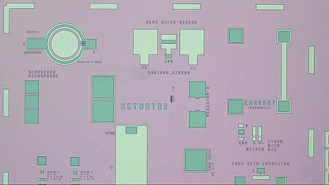
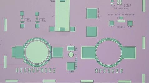
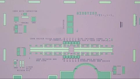
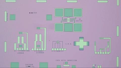
6 2015 MEMS MULTICHIP PROJECT DESIGN Page 6
7 MASK ORDER FORM Dr Fuller RIT mems-2015-final.gds mm x 16.5mm mems-2015-final x Page 7
8 MASK ORDER FORM DETAILS Reticle Number Reticle Name Design Layer # s Boolean Function Dark/ Clear 1 Poly1 1 None Clear 2 SacOx 2 None Clear 3 Anchor 3 3 Inverted Dark 4 No Implant 15 None Clear 5 Poly2 4,16 4 AND (16 Inverted) Clear 6 Cut 6 6 Inverted Dark 7 Metal 7 None Clear 8 Release 5 Inverted Dark Comment Design Layer 9 Out (outline) is not used. It is only for placement of projects on the multi-project reticle template. cp <filename>.gds /dropbox/masks Page 8
9 MASK PROCESS FLOW Data Prep CAD IC Graph by Mentor Graphics GDSII CATS Computer Aided Transcription Software MEBES File MEBES Job Etch Cr Inspect Develop Expose Coat Plate Maskmaking Inspect Clean Ship out This process can take weeks and cost between $1000 and $20,000 for each mask depending on the design complexity. Page 9

10 MEBES - Manufacturing Electron Beam Exposure System The masks were made using the MEBES electron beam writer at RIT. This tools is capable of writing on glass or quartz plates or wafers with spot size down to 0.1um. Page 10


11 CLEAR FIELD RETICLE FOR ASML Poly One Non-Chrome Side Metal Chrome Side Page 11
12 SURFACE MEMS 2015 PROCESS 1. Starting wafer 2. PH03 level 0, Marks 3. ET29 Zero Etch 4. ID01-Scribe Wafer ID, D1 5. ET07 Resist Strip, Recipe FF 6. CL01 RCA clean 7. OX Å Oxide Tube 1 8. CV01 LPCVD Poly 5000Å 9. IM01 Implant P31, 2E16, 60KeV 10. PH03 level 1 Poly ET08 Poly Etch 12. ET07 Resist Strip, Recipe FF 13. CL01- RCA Clean 14. OX05 700Å Dry Oxide 15. CV02- LPCVD Nitride 4000Å 16. PH03 level 2 Anchor 17. ET29 Etch Nitride 18. ET07 - Resist Strip, Recipe FF 19. CL01 RCA Clean 20. CV03-TEOS SacOx Dep 1.75um 21. PH03 level 3 SacOx Define 22. ET06 - wet etch SacOx Define Etch 23. ET07- Resist Strip, Recipe FF 24. CL01 RCA Clean 25. CV01-LPCVD Poly 2um, 140 min 26. PH03 - level 4 No Implant 27. IM01-P31 2E16 100KeV 28. ET07 Resist Strip, Recipe FF 29. CL01 RCA Clean 30. OX05-500Å pad oxide 31. CV Å nitride 32. PH03 - level 5 Poly2 33. ET29 Plasma Etch Nitride 34. ET06 Wet Etch pad oxide 35. ET68 - STS Etch Poly2 36. ET07 - Resist Strip, Recipe FF 37. PH03 level 6 Contact Cut 38. ET29 Etch Nitride Contact Cut 39. ET06 Etch Oxide Contact Cut 40. ET07 Resist Strip, Recipe FF CL01 RCA Clean two HF 42. ME01 Metal Deposition - Al 43. PH03 level 7 Metal 44. ET55 Metal Etch - wet 45. ET07 Resist Strip 46. PH03 level 8 Release 47. ET66 Final SacOx Etch 48. ET07 - Resist Strip, Recipe FF 49. SEM1 Pictures 50. TE01 - Testing Page 12


13 ZERO ETCH AND PHOTORESIST STRIP Today s Goal: Coat the wafers with photoresist, expose with ASML stepper, develop and plasma etch ASML alignment marks on six wafers. Etch Silicon using Drytek Quad 482 Etcher Cleaning of chamber for 5 min. in 02 plasma Etching the device wafer for 2 min. in CF4, CHF3 and O2 plasma Inspection of alignment marks on wafer Removal of Photoresist using GaSonics - (recipe FF) Microscope images of alignment marks before and after P.R. removal Before P.R. removal After P.R. removal Drytek Quad GaSonics PR Asher Authors: Abhinav, Nikhil, Ranjana, Shruthi, Yamini October 19, 2015 Page 13

 Procedure used to grow 6500A of oxide Measured Oxide Thickness: Mean : 6597.")
14 RCA CLEAN AND OXIDE GROWTH Today s Goal: Remove organic and metallic contaminants from wafers with RCA clean, steam oxide growth of 6500Å of oxide in Bruce Tube 1. Performed step 6: CL01 (RCA clean) Cleaned four wafers from lot Processed through SRD afterwards Adam developed and etched the other two wafers in the lot Performed step 7: OX04 (oxide growth) Procedure used to grow 6500A of oxide Measured Oxide Thickness: Mean : Å Std Dev. = 0.38% CL01 RCA Clean Authors: Mattias Herrfurth, Corey Shay OX04 oxide growth October 20, 2015 Page 14
15 LPCVD POLY DEPOSITION Today s Goal: Deposit polysilicon using the ASM LPCVD Tube 2 for a target thickness of 5000 Å. Step 8: CV01 LPCVD Poly 5000A - 3 wafers were done during this time - Other 3 wafers were processed Friday morning Parameters sccm of SiH 4 - Time: 36 mins - Temp: 650 C Wafer ID Mean Thickness (A) Standard Deviation (%) D D D Results of Poly Deposition Loading Wafer into the ASM LPCVD Tube 2 Authors: Adam Banees, Dustin Schroeder October 22, 2015 Page 15

 Standard Deviation (%) D1 5108.4 27.")

16 POLY THICKNESS MEASUREMENT Today s Goal: Measure the mean and the standard deviation of the poly thickness of 3 of the wafers using the SpectraMap Auto SM300. Target thickness was 5000Å. Wafer ID Mean Thickness (Å) Standard Deviation (%) D D D Wafer Topology Output of SpectraMap Loading Wafer into the SpectraMap Authors: Megan Ehrhart, Miaotian Wang October 23, 2015 Page 16

17 ION IMPLANTATION Today s Goal: Ion Implant of P31 ions using the Varian 350D ion implanter. Setting up the Varian 350D Ion Implanter Author: Aslesh Shetty October 23, 2015 Page 17


18 ION IMPLANT POLY 1 Today s Goal: Implant Poly1 with Phosphorus at 2e16 Dose. Time spent to achieved this dose was calculated. Dose Area q time = I Dose: 2e16 ions/cm 2 Area: 196 cm 2 q: 1.6e-19 C I: 1mA time = sec ~ 10.5 minutes Before and After Implant Wafer going into Ion Implanter Authors: Megan Ehrhart, Miaotian Wang October 23, 2015 Page 18


19 PHOTORESIST COATING FOR POLY1 PATTERNING Today s Goal: Coat the wafers with photoresist, P.R., measure thickness of the coating, expose with ASML stepper, post exposure bake and post development hard bake. Coated device and dummy wafers with P.R. Recipe Standard coat, 3250 RPM, 30 sec. Photoresist OIR 620 Measured thickness of P.R., SpectraMap Expose P.R. with ASML stepper Dose 250mJ/cm 2, Focus Offset 0.5 μm, NA 0.48 Post Exposure bake C, 60 sec. Post development hard bake C P.R. Thickness Data from SpectraMap Gives Mean = 10200Å P.R. Overlay and Resolution Pattern for Poly 1 Authors: Abhinav, Nikhil, Ranjana, Shruthi, Yamini October 26, 2015 Page 19


20 Wafers 5 and 6 poly etched on Drytek Quad. Recipe: FACCPOLY SF6: 30 sccm CHF3: 30 sccm O2: 5 sccm Ar: 0 sccm Pressure: 40mT RF Power: 160w Etch Rate: 1250 A/min POLY 1 ETCH AND RESIST STRIP Today s Goal: Etch Poly 1 with the Drytek Quad and strip the resist with an oxygen plasma produced in a GasSonics Aura 1000 Asher. Wafer 6 over etched, field oxide reduced to 5500Å, green. Wafer 5 etched for 4 min 30 sec with field oxide of 6100Å. Carnation pink. Chamber Plasma During Poly Etch Authors: Corey Shay, Mattias Herrfurth Chamber 2, O2 clean done before processing wafers. October 27, 2015 Page 20


21 AFTER POLY 1 ETCH AND RESIST STRIP Pictures of some of the devices on wafer 5 after etch and resist strip Authors: Corey Shay, Mattias Herrfurth October 27, 2015 Page 21


 from SC1.")


22 RCA CLEAN AND 700Å OXIDE GROWTH Today s Goal: Remove organic and metallic contaminants from wafers with RCA clean, Dry oxide growth of 700Å in Bruce Tube 4. Performed Step 13: CL01- RCA Clean SC1 <10min> Remove Organic components. HF <30s> Remove Oxide (5nm) from SC1. SC2 <10min> Remove metallic components. Spin/Rinse Dry Performed Step 14: CV03 OX05 700Å Dry Oxide An etch stop and pad oxide for subsequent silicon nitride deposition. Recipe 270; 1h 33min, Soak. Dry O2 CL01- RCA Clean Microelectronic Wafer Before Engineering Oxide Growth Loading Wafer into the Bruce Tube4 October 28, 2015 Authors: Miaotian Wang Page 22
 and ammonia")
23 4000 Å LPCVD NITRIDE DEPOSITION Today s Goal: Deposit nitride using the ASM LPCVD Tube 2 for a target thickness of 4000 Å. Step 15: CV Å LPCVD Nitride - 8 wafers total, 6 device wafers, 2 control wafers - C1: Si wafer with 780A of dry oxide - C2: Bare Si wafer Parameters - Dichlorosilane (H 2 SiCl 2 ) and ammonia (NH 3 ) - Time: 67 mins - Temp: 810 C Wafer ID Mean Thickness (A) Standard Deviation (%) C C Results of Nitride Deposition Authors: Adam Banees, Dustin Schroeder, Chris O Connell, Miotian Wang Loading Wafer into the ASM LPCVD Tube 2 October 29, 2015 Page 23

24 MEASURING REMAINING OXIDE THICKNESS Today s Goal: To find the thickness of the remaining oxide under the Nitride after etching the Nitride. Starting oxide was 700Å Procedure Coating photoresist Exposure in Lithography Post exposure bake Exposing to developing material Dry etching for? min. Measuring oxide thickness Measuring oxide thickness Oxide thickness measured with Nanometrics 210 Point Number Thickness (Å) Authors: Farzad Forouzandeh, Adam Wardas October 30, 2015 Page 24
25 DETERMINE NITRIDE ETCH RATE Today s Goal: Coat dummy wafer with negative photo resist and etch the nitride a little at a time to determine nitride etch rate. 1. Measure nitride thickness prior to etch using NanoSpec Optical Reflectance Spectrometer 2. Coat wafers with n-lof-2020 Image Reversal Resist, Use COATNLOF recipe on the SSI track 3. Expose on the ASML Stepper 4. Develop on SSI Track using recipe DEVNLOF 5. Etch in LAM490 plasma etcher using SF6 gas 6. Remove Photoresist NIT PreEtch (Å) 2min Etch (Å) 4min Etch (Å) After 6min Etch(Å) Center Top Left Bottom Right Average (Å) Average Etch Rate (Å/min) Å/min Å/min - Authors: Megan Ehrhart October 30, 2015 Page 25
26 ANCHOR PHOTO AND NITRIDE ETCH Today s Goal: Coat and expose photoresist for Anchor level, then etch nitride back using SF6 plasma Performed step 16: PH03 (photolithography coat, expose, and develop) Coated all wafers in lot with OiR-620 resist on SSI track Exposed on ASML stepper Stepper did not start up properly; had to reset several times Develop track was not operating; had to use CEE-100 spinner w/ CD-26 developer Note: Had to process through one wafer to test processes and work out kinks; by end of session only one wafer went through nitride etch Performed step 17: ET29 (nitride etch) Used LAM-490 w/ SF6 plasma to etch nitride First run didn t etch, needed to rerun After nitride etch, tried to measure oxide on poly w/ Nanospec, but material stack was too complex for measurement Performed step 18: ET07 (resist strip) Only performed on one wafer to check anchor etch Authors: Mattias Herrfurth, Corey Shay, Yamini Sodagum, Shruthi Venkateshan, Abhinav Mamidala November 3, 2015 Page 26


27 ANCHOR PHOTO AND NITRIDE ETCH PH03 SSI track coat resist PH03 Expose resist on ASML PH03 Develop on CEE-100 ET29 etch with LAM 490 Authors: Mattias Herrfurth, Corey Shay, Yamini Sodagum, Shruthi Venkateshan, Abhinav Mamidala November 3, 2015 Page 27


28 RECIPES FOR ASML STEPPER AND LAM 490 Recipe for nitride etch as displayed on LAM 490 Recipe for ASML Stepper: Dose = 250 mj/cm 2 Focus Offset = 1µm NA = 0.48 σ = Recipe for nitride etch in LAM 490: Pressure = 260 mtorr RF Top = 125 Watts Gap = 1.65 cm SF6 flow = 200 sccm Time = 7 min / wafer Plasma generated in LAM490 chamber Authors: Mattias Herrfurth, Corey Shay, Yamini Sodagum, Shruthi Venkateshan, Abhinav Mamidala November 3, 2015 Page 28


29 DEVICE IMAGES AFTER RESIST STRIP Images of devices after anchor photo, etch, and resist strip Authors: Mattias Herrfurth, Corey Shay, Yamini Sodagum, Shruthi Venkateshan, Abhinav Mamidala November 3, 2015 Page 29


30 AFTER NITRIDE ETCH AND RESIST STRIP Green Anchor ~500Å Oxide on Poly1 on 6500Å Oxide on Silicon Pink Nitride on 7200Å Oxide on Silicon Alignment Mark - Anchor White Nitride on 700Å Oxide on Poly1 on 6500Å Oxide on Silicon Authors: Miaotian Wang, Nikhil Ratakonda November 4, 2015 Page 30


31 RCA CLEAN AND PEVCD OXIDE FROM TEOS Today s Goal: Remove organic and metallic contaminants from wafers with RCA clean, PECVD of TEOS Silicon Dioxide of 1.75um in AME P5000 Chamber A. Performed Step 19: CL01 - RCA Clean SC1 <10min> Remove Organic components. HF <30s> Remove Oxide (25nm) from SC1. SC2 <10min> Remove metallic components. Spin/Rinse Dry Same as Page 22 Performed Step 20: CV03 - TEOS SacOx 1.75um Heated chamber at 390 C RF Plasma + TEOS Deposition rate calc. by setting 120s for 1um on Blank Wafer Result: Mean = Å; Std Dev. = 2.209% Recipe - 120s for 1um, then 90s for 0.75um Total 1.75um CL01- RCA Clean Spin Rinse Dry (SRD) CV03 AME P5000 After PECVD 1.75um Oxide Authors: Miaotian Wang, Nikhil Ratakonda November 4, 2015 Page 31


32 SACOX PHOTO Today s Goal: Coat and expose photoresist for SacOx. Performed step 21: level 3 SacOx Define Applied MICROPOSIT S1827 Photoresist - Thicker resist than OIR Necessary due to increasingly complex topography ASML Stepper SacOx Step - E = 525 mj/cm2 - Focus Offset = Numerical Aperture = Sigma Outer = ASML Stepper Control Terminal Manually applying S1827 resist Authors: Dustin Schroeder, Christopher O Connell, Adam Banees November 5, 2015 Page 32


33 RESIST STRIP, TESTING TO VERIFY ETCH WORKED Today s Goal: Removed photo resist and tried to measure Poly1 resistor without success. Will have to investigate more. 1. Etch with Using 5.2:1BOE for 10 minutes. 2. Rise for 5 minutes in DI water 3. Spin dry for 5 minutes. When measuring a number of the Poly1 resistors, we got an open. However, when we connected both probes to a large pad, we got a low resistance. Putting Wafer in 5.2:1BOE Spin, Rinse, Dry (SRD) Tool Used to Dry a Boatload of Wafers Authors: Megan Ehrhart November 6, 2015 Page 33

34 TESTING TO MEASURE POLY1 RESISTANCE Today s Goal: To find out if the anchor etch was done properly. Probe poly1 at the anchor holes at the ends of resistor structures and measure resistance. If infinite then etch was not complete down to the surface of Poly1. Finite resistance is good. Testing gave result: infinite resistance (oxide and nitride is not etched properly) We reworked the wafer, etch more. Coat with photoresist Do Photolithography(Anchor Mask) Manual Developing Dry etching of nitride (1 min) Checked color under microscope Oxide etch using the BOE (10 min) Testing again. Still infinite resistance Probe Station and Microscope Display Showing Resistor being Tested Authors: Ankur November 9, 2015 Page 34
 Thickness of different layers is measured at different locations using Tencor P2 Profilometer.")
 Still the resistors read infinite resistance In large pads two probes 100um apart read a resistance of 30 ohms.")
35 STRIP PHOTORESISTAND THICKNESS MEASUREMENT Today s Goal: Removal of Photoresist using GaSonics, measuring thickness of the coatings to determine if the etch depths seem correct. Removal of Photoresist using GaSonics - (recipe FF) Thickness of different layers is measured at different locations using Tencor P2 Profilometer. Wafers were also tested for electrical conductivity None of the resistor structures showed conductivity Profile measurements indicate presence of Poly1at all locations. (does not seem to be over etched) Still the resistors read infinite resistance In large pads two probes 100um apart read a resistance of 30 ohms. Still the resistors read infinite resistance Decided to move forward with the remaining wafers 7597A Thickness measurement by Profilometer 6795A Thickness measurement by Profilometer Authors: Abhinav, Nikhil, Ranjana, Shruthi, Yamini November 09, 2015 Page 35

 Results show no electrical conduction thus oxide still remains in the anchor holes Etch wafers in BOE 5.2:1 for another 5 min.")
36 SACOX ETCH AND RESISTOR TESTING Today s Goal: Etch the SacOx on the remaining 5 wafers. Test to make sure the etch goes down to Poly1 in the Anchor Holes. Test resistors to see if they were working correctly. If they are working correctly then next step is strip photoresist. If not etch longer in Buffered Oxide Etch and test resistors again. SacOx Etch ET06 Step 22 Etch wafer in BOE 5.2:1 solution for 10 min. Test Resistors (see next page) Results show no electrical conduction thus oxide still remains in the anchor holes Etch wafers in BOE 5.2:1 for another 5 min. Test Resistors (see next page) Results show ~ correct resistance values. Etch remaining wafers for total of 15 min. SRD Spin, Rinse, Dry. Authors: Abhinav, Nikhil, Ranjana, Shruthi, Yamini 1.75um SacOx etch in 5.2:1 BOE November 10, 2015 Page 36


37 TESTING REMOVAL OF NITRIDE AND OXIDE IN ANCHOR HOLES OVER POLY1 Electrical Test involves placing two probes on the wafer and connecting to the HP 4145 Semiconductor Parameter Analyzer set up to sweep the voltage from -20 to +20 volts and measuring the current. The slope is 1/R. Any reasonable value is good. Probes at both ends of Resistor Structure Two Probes on Same Anchor hole to Poly1 Slope = R = 1/Slope = 64 Ω I I -20V 0 +20V I vs V I vs V Slope = R = 1/Slope = 300 Ω V Authors: Corey Shay Mattias Herfurth November 10, 2015 Page 37


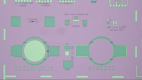
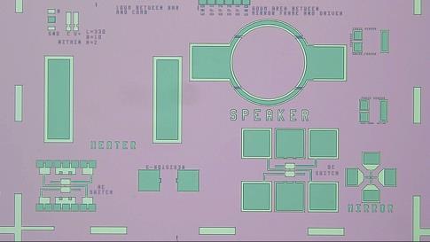
38 RESIST STRIP AND TAKE PICTURES Today s Goal: Resist strip with GasSonics Asher. Get all wafers ready for RCA Clean and Poly2 Resist Strip ET07 Step 23 Recipe FF runs recipe F twice for resist strip. Recipe F Pressure 2.0 Torr O2 4.5 LPM N 0.5 LPM Time 99 sec MEMS Switch 1 2 d 4 r Mirror 3 SacOx remains in center rectangle SacOx remains in circle of radius r with hole in center of diameter d to anchor a mirror of Poly2, electrostatic actuation with the 4 poly1 plates 1,2,3,4 Authors: Corey Shay, Mattias Herfurth, Adam Wardas November 10, 2015 Page 38

39 TESTING TO MEASURE POLY 1 RESISTANCE Today s Goal: Probe Poly 1 at the anchor holes at the ends of resistor structures and measure resistance. Electrical Test involves placing two probes on the wafer and connecting to the HP 4145 Semiconductor Parameter Analyzer set up to sweep the voltage from -20 to +20 volts and measuring the current. The slope is 1/R. Same as Page 37. I vs V (Wafer D3) -20V 0 +20V I vs V (Wafer D2) Probes at both ends of Resistor Structure Slope = m R D2 = 1/Slope = 296 Ω L/W ~10 Rhos ~30 ohms/sq -20V 0 +20V Slope = m R D3 = 1/Slope = 285 Ω Authors: Miaotian Wang EHRHART THERMOPILE November 11, 2015 Page 39
40 TESTING TO MEASURE POLY 1 RESISTANCE I vs V (Wafer D4) I vs V (Wafer D6) Slope = m R D4 = 1/Slope = 346 Ω -20V 0 +20V Slope = m R D6 = 1/Slope = 350 Ω -20V 0 +20V The cause of the difference might be that wafer D4, D6 deposited polysilicon (36min, 650 C) 1min longer than D2, D3 (35min, 650 C). (Refer to Page 15) Wafer ID Slope Resistance(Ω) D m 296 D m 285 D m 346 D m 350 Result of Electrical Test Authors: Miaotian Wang November 11, 2015 Page 40
41 LPCVD POLY 2 DEPOSITION Today s Goal: Deposit polysilicon using the ASM LPCVD Tube 2 for a target thickness of 1.75µm. Step: CL01 RCA Clean -Standard RCA clean was preformed, with addition of a 30s HF dip after SC1 and SC2 Step: CV01- LPCVD Poly 2µm - 4 wafers were processed with one TEOS control wafer - The fifth wafer is in rework Parameters -100 sccm of SiH 4 -Time: 130 mins -Temp: 650 C Wafer ID Mean Thickness (A) Standard Deviation (%) C TEOS Thickness on control before poly 2 deposition Loading Wafers into the ASM LPCVD Tube 2 Authors: Chris O Connell, Adam Banees, Dustin Schroeder, Adam Wardas November 12, 2015 Page 41
42 RCA CLEAN AND DEPOSITION OF POLY2 Today s Goal: Clean the wafers using RCA clean (with two HF dips) prior to deposition of Poly2 followed by LPCVD of 1.75um thick layer of polysilicon (Poly2). The second HF dip prior to the final DI rinse is to remove any chemically grown oxide from the SC2 (contains H2O2) on Poly1. We want Poly2 and Poly1 to be electrically connected at the anchor locations. Poly2 is deposited by LPCVD at 850 C with Silane (SiH4) at 300 mtorr for 140 min. Measure Poly2 thickness using the Spectromap on a test wafer that had only oxide on it. Results gave average Poly 2 thickness of 1.70um. Authors: Dr. Fuller, Adam Wardas November 12, 2015 Page 42
 was used so as to not effect the current structure with large step heights to coat. 1. HMDS vapor prime and bake at 140 C for 60 seconds 2.")
43 RESIST COATING FOR NO-IMPLANT LAYER Today s Goal: Using the SSI Tack, apply the resist coating for the no implant layer. Photoresist 1827 (a thicker resist) was used so as to not effect the current structure with large step heights to coat. 1. HMDS vapor prime and bake at 140 C for 60 seconds 2. Coat wafers with 1827 Resist 3. Spin at 2500 RPM 4. Bake at 90 C for 60 seconds SSI Track Authors: Megan Ehrhart November 14, 2015 Page 43


44 RESIST EXPOSE AND DEVELOP NO-IMPLANT LAYER Today s Goal: Expose and Develop No-Implant Layer.Take Pictures Pink pattern is photoresist regions not to be implanted. Authors: Abhinav, Nikhil, Ranjana, Shruthi, Yamini November 14, 2015 Page 44


45 ION IMPLANTATION P31, 100KEV Today s Goal: Ion implantation of Phosphorous at 100 KeV with Dose of 2E15 Ion implant with Dose of 2E15 was carried out with beam current of 300 Μa. Dose Area Charge Beam Current Area of 6 wafer = 196 cm 2 Time of Implant = Time = 2E E E 6 ~ 35 Minutes/wafer Detector ~175mm diameter with 10mm hole in center is used to set up the beam scan. Horizontal scan current and vertical scan current is displayed with an oscilloscope. The M shape shows the scan will pass across the center of the detector and thus the scan will be centered on the wafer. Authors: Abhinav, Nikhil, Ranjana, Shruthi, Yamini Ion Beam Set Up November 16, 2015 Page 45
 SRD last step Performed step 30 Thin oxide growth (Dry O 2 ) Recipe")
46 RESIST STRIP, RCA CLEAN AND THIN OXIDE GROWTH Today s Goal: Clean wafers of metallic and organic contaminants for the purpose of preparing them for a dry O 2 oxide growth of 500Å Performed step 29 RCA Clean SC1 5000mL DI Water, 300mL NH 4 OH, 300mL H 2 O 2 SC2 5000mL DI Water, 300mL HCl, 300mL H 2 O 2 HF Bath 50:1 (H 2 O:HF) SRD last step Performed step 30 Thin oxide growth (Dry O 2 ) Recipe #250 RCA clean process flow Authors: Mattias Herrfurth, Corey Shay November 17, 2015 Page 46


47 PROCESS FLOW FOR RCA CLEAN OXIDE GROWTH SC1 Bath SC2 Bath Spin Rinse Dryer Dry Oxide Growth Authors: Mattias Herrfurth, Corey Shay November 17, 2015 Page 47
 Mean : 512.09 A Std Dev. = 4.")
 60 sccm of DCS (SiH 2 Cl 2 ); 148 sccm of NH 3 Time: 35 mins Temp: 810 ºC Measured Nitride Thickness: Mean : 1978.8 A Std Dev. = 3.")
48 2000 A LPCVD NITRIDE DEPOSITION Today s Goal: Deposit nitride using the ASM LPCVD Tube 2 for a target thickness of 2000 A. Measured Oxide Thickness: (Step 30) Mean : A Std Dev. = 4.945% Step 31: CV02 LPCVD Nitride 2000A 11 wafers total, 4 device wafers, 6 control wafers and 1 blank wafer Parameters TubeMKS: 300 mtor (Deposition pressure) 60 sccm of DCS (SiH 2 Cl 2 ); 148 sccm of NH 3 Time: 35 mins Temp: 810 ºC Measured Nitride Thickness: Mean : A Std Dev. = 3.971% Device Wafer after LPCVD 2000 A Nitride Blank Wafer after LPCVD 2000 A Nitride Authors: Miaotian Wang November 18, 2015 Page 48

49 POLY 2 LAYER LITHOGRAPHY WITH ASML Today s Goal: Due to issues with some equipment, only one wafer (D3) was able to be exposed during this lab. The recipe was modified slightly, see below, to increase the focus because there are more layers on the wafer now. ASML Setup Parameters: Energy: 525 mj/cm 2 Focus: +4.0 NA: 0.48 Sigma: 045 Note: these settings did not turn out good ASML Authors: Megan Ehrhart October 30, 2015 Page 49


50 ETCHING OF NITRIDE, PAD OXIDE, & POLYSILICON Today s Goal: Etching of Silicon Nitride, Pad Oxide and Polysilicon Nitride etching of all the wafers using LAM 490 Recipe used FNIT m T, 4.54 Seconds for nitride etch, SF6 200SCCM Oxide etching of D3 wafer BOE 5.2:1 - for 2 minutes Deionized water - for 5 minutes Poly-silicon etching Drytek Quad Chamber 2 Recipe FACPOLY step 2 Etch rate was found to be slow, didn t etch polysilicon completely in 10 minutes. Etched another 10 minutes Results were not good. Think the lithography was not good. So we plan to do a focus-exposure matrix to determine best focus and exposure. Then redo the lithography Microelectronic prior Engineering to Poly2 etch on Lam 490 Plasma Intensity Vs. Time for Nitride etching Polysilicon etching starts to clear at the edge of the wafer after 10 mins remaining wafers November 23, 2015 Authors: Abhinav, Nikhil, Ranjana, Shruthi, Yamini Nitride etch Pad Oxide etch Poly removed from periphery of wafer Page 50


51 Today s Goal: Plasma etch poly 2 prior. PLASMA ETCH POLY 2 Wafer D4 processed etched 1. Post development 140C for 60s. 2. Plasma etch Poly 2 hole with Drytek Quad Recipe: FACCPOLY Chamber 2 for 18 min 3. Strip resist with GaSonics Asher Recipe: FF Poly 2 for a MEMS Speaker Authors: Corey Shay, Mattias Herrfurth, Adam Wardas Poly 2 over SacOx for A MEMS Switch. December 1, 2015 Page 51


52 PHOTORESIST COATING FOR POLY2 PATTERNING Today s Goal: Coat the wafers with photoresist, expose with ASML stepper and develop two wafers. Step 32: PH03 - level 5 Poly2 Coated all wafers with S1827 resist on SSI track ~ 3um thick Expose P.R. with ASML stepper Exposure Dose = 475 mj/cm 2, Focus Offset = -2μm ~ for D6 Exposure Dose = 350 mj/cm 2, Focus Offset = -2μm ~ for D3 Post Exposure bake C, 200 sec. GaSonics PR Asher Manually applying S1827 resist Authors: Miaotian Wang December 2, 2015 Page 52
 D6")


53 REDUCING EXPOSURE IMPROVES RESIST IMAGE D6 Exposure Dose (mj/cm 2 ) D6 D D3 D6 focused on Substrate bottom of Resist D6 focused on Poly 2 Top of Resist D6 D3 focused on Substrate bottom of Resist D3 focused on Poly 2 Top of Resist D3 Authors: Miaotian Wang December 2, 2015 Page 53

 2 = > 1.0 µm for NA = 0.")
54 ASML 5500/200 NA = 0.48 to 0.60 variable = 0.35 to 0.85 variable With Variable Kohler, or Variable Annular illumination Resolution = K1 l/na = ~ 0.35µm for NA=0.6, =0.85 Depth of Focus = k 2 l/(na) 2 = > 1.0 µm for NA = 0.6 i-line Stepper l = 365 nm 22 x 27 mm Field Size Page 54
55 DOING A FOCUS EXPOSURE TEST Today s Goal: We need to determine the best focus and exposure for the thick resist (S1827 ~3um) used on poly2. F = -3.0 Example: Depth of Focus = k 2 l/(na) 2 l = 365nm. Let k 2 = 0.63 and NA = 0.48 Gives Depth of Focus = 1.0um (so pick step size of 1.0um) F = 0.0 Best Best found today with S1827 resist F= E= 400 mj/cm2 F = mj/cm2 Authors: Stephanie Bolster December 3, 2015 Page 55


56 PICTURES FROM FOCUS EXPOSURE TEST F=0.0 F=+2 F=+1 F=-1 F=-2 F=-3 Top Row: Microscope Focused at Top of Photoresist Bottom Row: Microscope Focused at Bottom of Photoresist S1827 ~3um Photoresist, All Exposure Dose at 400 mj/cm2 Authors: Stephanie Bolster December 8, 2015 Page 56
57 SETTING FOCUS FOR ASML STEPPER / THICK RESIST Focus of 0.0 is the best focus setting experimentally determined using a ~1um thick resist on a blank wafer. A stage gap sensor is used to position the surface of the wafer at a repeatable starting distance from the bottom of the lens. The gap for best focus is called zero. If the stepper job calls for a focus offset the stage height is moved an additional amount from best focus equal to the offset in µm, a positive offset makes the gap bigger, a negative offset makes the gap smaller. For positive resist the profiles might look like this for thick resist. F = +2.0 F = 0.0 Lens Focus offset = +2.0 PR Thickness = 4µm Lens Focus offset = 0.0 PR Thickness = 4µm Lens Focus offset = -2.0 Top of PR Top of PR Top of PR F = -2.0 PR Thickness = 4µm Authors: Stephanie Bolster December 3, 2015 Page 57


58 POLYSILICON2 ETCHING Today s Goal: To etch Polysilicon2 on remaining wafers Using the dry tech quad tool, Recipe FACPOLY Chamber 2, Time= 18 minutes Adam at Dry Tech Quad Wafer Bfore Poly Etch Wafer After Poly Etch Authors: Ankur December 5, 2015 Page 58
: Presure: 2 Torr Oxygen: 4.5 LPM Nitrogen: 0.")
59 REMOVE PHOTORESIST Today s Goal: On wafer D3, the photoresist for Poly2 was removed, after the wafer was etched correctly. Remove Photoresist (Recipe FF): Presure: 2 Torr Oxygen: 4.5 LPM Nitrogen: 0.5 LPM Time: 99 seconds two times GaSonics Oxygen Plasma Asher Authors: Megan Ehrhart December 4, 2015 Page 59
 1.")

60 COAT AND EXPOSE CONTACT PHOTORESIST Today s Goal: On wafer D3, the Photoresist for the Contact Cut layer was coated and exposed. Coat with Photoresist (recipe MEMs Coat) 1. Coat with HMDS and bake at 140 C for 60 seconds 2. Coat wafers with 1827 Resist 3. Spin at 2500 RPM 4. Bake at 90 C for 60 seconds SSI Track ASML Setup Parameters: Energy: 400 mj/cm 2 Focus: -0.5 NA: 0.6 Sigma: 0.7 ASML Authors: Megan Ehrhart December 4, 2015 Page 60

61 CONTACT CUT LITHO, NITRIDE AND OXIDE ETCH Today s Goal: To perform Level 6, Contact cut lithography and Nitride and Oxide etch on wafers D2, D4, D6. Manual coating of PR S1827 Contact cut lithography with- Dose- 400 mj/cm2 Focus offset 0.5 micro σ = 0.7 Post bake at 140 C Nitride Etch Recipe Factory Nitride Etch, Lam 490 Gas used SF6 Time (3 minutes for etch + 1 minute over etch)/wafer Buffered Oxide Etch BOE 5.2:1 - for 2 minutes Deionized water - for 5 minutes, SRD Wafer after Oxide etch Authors: Abhinav, Nikhil, Ranjana, Shruthi, Yamini December 07, 2015 Page 61

62 TESTING TO MEASURE POLY 2 RESISTANCE Today s Goal: Probe Poly 2 at the anchor holes at the ends of resistor structures and measure resistance. Test involves placing two probes on the wafer and connecting to the HP 4145 Semiconductor Parameter Analyzer set up to sweep the voltage from -10 to +10 volts and measuring the current. The slope is 1/R. I vs V Probes at both ends of Slope=0.6277m Resistor Structure R=1/Slope=1.59K If L/W=3, Rhos = 530 ohms/sq Note: no implant makes W smaller than it looks Authors: Aslesh Shetty, Naresh Bakhtiani,Nikhil, Adam Wardas December 4, 2015 Page 62


63 TESTING TO MEASURE POLY 2 RESISTANCE D4 Today s Goal: Probe Poly 2 at the anchor holes at the ends of resistor structures and measure resistance. Test involves placing two probes on the wafer and connecting to the HP 4145 Semiconductor Parameter Analyzer set up to sweep the voltage from -10 to +10 volts and measuring the current. The slope is 1/R. Gas Flow Sensor Slope=0.0170m R=1/Slope=58.8K Wafer D4 Slope=0.0103m R=1/Slope=97K Wafer D4 Why are these R s so high? Authors: Aslesh Shetty, Naresh Bakhtiani,Nikhil, Adam Wardas Slope=0.2603m R=1/Slope=3.84K Wafer D4 Note: this resistor is poly1 to poly2 to poly1 December 4, 2015 Page 63
64 MORE TEST RESULTS WAFER D6 Test involves placing two probes on the wafer and connecting to the HP 4145 Semiconductor Parameter Analyzer set up to sweep the voltage from -10 to +10 volts and measuring the current. The slope is 1/R. Why are these so much lower than D4? Chevron Thermal Actuator with resistance 500ohms (Yamini s device) Peltier resistor R1 = 202 Ohm, R2 = 215 Ohm December 7, 2015 Page 64
 + 1 control wafer with tape for measurement Time")
 Arc detect count -> 40 Pre-sputtering: 5 min same power - Arc detect count -> 3")

65 ALUMINUM METAL DEPOSITION Today s Goal: Deposit Al using CVC601 Sputter tool for a target thickness of 10,000Å. Step 42: ME01 Metal Deposition Al 4 device wafers (D2, D3, D4, D6 ) + 1 control wafer with tape for measurement Time ~ 34 min 2000 Watts for ~300 Å/min ( Sputtering power ) Pressure 5 mt ( Sputtering Pressure ) Argon Flow 28 sccm ( to set the Sputtering Pressure ) Arc detect count -> 40 Pre-sputtering: 5 min same power - Arc detect count -> 3 Remove contaminants from target expose to atmosphere (Al 2 O 3, AlN, etc.). Target Wafer after Sputtering Inside the Vacuum Chamber with the Platen Inside the Vacuum Chamber without the Platen Authors: Miaotian Wang December 9, 2015 Page 65
66 CURRENT WAFER STATUS December 9, 2015 D1 D2 D3 D4 D5 D6 Next Step Dead (Over etched the nitride. There is no contact to Poly1.) Step 43 PH03 Aluminum Photolithography Step 43 PH03 Aluminum Photolithography Step 43 PH03 Aluminum Photolithography Measure P1 Resistor then Step 24. CL01 Step 43 PH03 Aluminum Photolithography Authors: Megan Ehrhart December 8, 2015 Page 66
67 SURFACE MEMS 2015 PROCESS 1. Starting wafer 2. PH03 level 0, Marks 3. ET29 Zero Etch 4. ID01-Scribe Wafer ID, D1 5. ET07 Resist Strip, Recipe FF 6. CL01 RCA clean 7. OX Å Oxide Tube 1 8. CV01 LPCVD Poly 5000Å 9. IM01 Implant P31, 2E16, 60KeV 10. PH03 level 1 Poly ET08 Poly Etch 12. ET07 Resist Strip, Recipe FF 13. CL01- RCA Clean 14. OX05 700Å Dry Oxide 15. CV02- LPCVD Nitride 4000Å 16. PH03 level 2 Anchor 17. ET29 Etch Nitride 18. ET07 - Resist Strip, Recipe FF 19. CL01 RCA Clean 20. CV03-TEOS SacOx Dep 1.75um 21. PH03 level 3 SacOx Define 22. ET06 - wet etch SacOx Define Etch 23. ET07- Resist Strip, Recipe FF 24. CL01 RCA Clean 25. CV01-LPCVD Poly 2um, 140 min 26. PH03 - level 4 No Implant 27. IM01-P31 2E16 100KeV 28. ET07 Resist Strip, Recipe FF 29. CL01 RCA Clean 30. OX05-500Å pad oxide 31. CV Å nitride 32. PH03 - level 5 Poly2 33. ET29 Plasma Etch Nitride 34. ET06 Wet Etch pad oxide 35. ET68 - STS Etch Poly2 36. ET07 - Resist Strip, Recipe FF 37. PH03 level 6 Contact Cut 38. ET29 Etch Nitride Contact Cut 39. ET06 Etch Oxide Contact Cut 40. ET07 Resist Strip, Recipe FF CL01 RCA Clean two HF 42. ME01 Metal Deposition - Al 43. PH03 level 7 Metal 44. ET55 Metal Etch - wet 45. ET07 Resist Strip 46. PH03 level 8 Release 47. SA01 Saw Wafer ½ Way 48. Special Soap Clean 49. ET66 Final SacOx Etch 50. ET07 - Resist Strip with Acetone 51. Rinse and Dry w Isopropyl Pull 52. TE01 wafer level testing 53. SEM1 Pictures 54. Packaging and Testing Page 67
MEMS Surface Fabrication
 ROCHESTER INSTITUTE OF TECHNOLOGY MICROELECTRONIC ENGINEERING MEMS Surface Fabrication Dr. Lynn Fuller webpage: http://people.rit.edu/lffeee Electrical and Microelectronic Engineering Rochester Institute
Bulk MEMS Fabrication Details Dr. Lynn Fuller, Casey Gonta, Patsy Cadareanu
 ROCHESTER INSTITUTE OF TECHNOLOGY MICROELECTRONIC ENGINEERING Bulk MEMS Fabrication Details Dr. Lynn Fuller, Casey Gonta, Patsy Cadareanu Webpage: http://people.rit.edu/lffeee 82 Lomb Memorial Drive Rochester,
Surface MEMS Fabrication Details Dr. Lynn Fuller, Adam Wardas, Casey Gonta, Patsy Cadareanu
 ROCHESTER INSTITUTE OF TECHNOLOGY MICROELECTRONIC ENGINEERING Surface MEMS Fabrication Details Dr. Lynn Fuller, Adam Wardas, Casey Gonta, Patsy Cadareanu Webpage: http://people.rit.edu/lffeee 82 Lomb Memorial
Bulk MEMS Fabrication Blog 2017 Dr. Lynn Fuller, Casey Gonta, Patsy Cadareanu
 ROCHESTER INSTITUTE OF TECHNOLOGY MICROELECTRONIC ENGINEERING Bulk MEMS Fabrication Blog 2017 Dr. Lynn Fuller, Casey Gonta, Patsy Cadareanu Webpage: http://people.rit.edu/lffeee 82 Lomb Memorial Drive
Photoresist Coat, Expose and Develop Laboratory Dr. Lynn Fuller
 ROCHESTER INSTITUTE OF TECHNOLOGY MICROELECTRONIC ENGINEERING Photoresist Coat, Expose and Develop Laboratory Dr. Lynn Fuller Webpage: http://www.rit.edu/lffeee 82 Lomb Memorial Drive Rochester, NY 14623-5604
Summary of Selected EMCR650/731 Projects for Jeremiah Hebding Dr. Lynn Fuller
 ROCHESTER INSTITUTE OF TECHNOLOGY MICROELECTRONIC ENGINEERING Summary of Selected EMCR650/731 Projects for 2004-2005 Jeremiah Hebding Dr. Lynn Fuller Motorola Professor 82 Lomb Memorial Drive Rochester,
Summary of Selected EMCR732 Projects for Spring 2005 Mike Aquilino Dr. Lynn Fuller
 ROCHESTER INSTITUTE OF TECHNOLOGY MICROELECTRONIC ENGINEERING Summary of Selected EMCR732 Projects for Spring 2005 Mike Aquilino Dr. Lynn Fuller Motorola Professor 82 Lomb Memorial Drive Rochester, NY
Dr. Lynn Fuller, Motorola Professor Steven Sudirgo, Graduate Student
 ROCHESTER INSTITUTE OF TECHNOLOGY MICROELECTRONIC ENGINEERING Bulk Micromachined Pressure Sensor Dr. Lynn Fuller, Motorola Professor Steven Sudirgo, Graduate Student 82 Lomb Memorial Drive Rochester, NY
2015 EE410-LOCOS 0.5µm Poly CMOS Process Run Card Lot ID:
 STEP 0.00 - PHOTOMASK #0- ZERO LEVEL MARKS Starting materials is n-type silicon (5-10 ohm-cm). Add four test wafers labeled T1-T4. T1 and T2 will travel with the device wafers and get all of the processing
CMOS Factory Laboratory
 ROCHESTER INSTITUTE OF TECHNOLOGY MICROELECTRONIC ENGINEERING CMOS Factory Laboratory Dr. Lynn Fuller Webpage: http://people.rit.edu/lffeee 82 Lomb Memorial Drive Rochester, NY 14623-5604 Tel (585) 475-2035
Wafer Cleaning and Oxide Growth Laboratory Dr. Lynn Fuller Webpage:
 ROCHESTER INSTITUTE OF TECHNOLOGY MICROELECTRONIC ENGINEERING Wafer Cleaning and Oxide Growth Laboratory Dr. Lynn Fuller Webpage: http://www.rit.edu/~lffeee 82 Lomb Memorial Drive Rochester, NY 14623-5604
Microelectronic Device Instructional Laboratory. Table of Contents
 Introduction Process Overview Microelectronic Device Instructional Laboratory Introduction Description Flowchart MOSFET Development Process Description Process Steps Cleaning Solvent Cleaning Photo Lithography
Dr. Lynn Fuller Webpage:
 ROCHESTER INSTITUTE OF TECHNOLOGY MICROELECTRONIC ENGINEERING Microelectromechanical Systems (MEMs) Process Integration Dr. Lynn Fuller Webpage: http://people.rit.edu/lffeee 82 Lomb Memorial Drive Rochester,
LAM 490 Etch Recipes. Dr. Lynn Fuller
 ROCHESTER INSTITUTE OF TECHNOLOGY MICROELECTRONIC ENGINEERING LAM 490 Etch Recipes Dr. Lynn Fuller Professor, Webpage: http://people.rit.edu/lffeee 82 Lomb Memorial Drive Rochester, NY 14623-5604 Tel (585)
Surface micromachining and Process flow part 1
 Surface micromachining and Process flow part 1 Identify the basic steps of a generic surface micromachining process Identify the critical requirements needed to create a MEMS using surface micromachining
RIT s Sub-CMOS Process (Leff < 1.0 µm) Dr. Lynn Fuller Suraj Bhaskaran and Ivan Puchades
 Dr. Lynn Fuller Suraj Bhaskaran and Ivan Puchades") ROCHESTER INSTITUTE OF TECHNOLOGY MICROELECTRONIC ENGINEERING RIT s (Leff < 1.0 µm) Dr. Lynn Fuller Suraj Bhaskaran and Ivan Puchades 82 Lomb Memorial Drive Rochester, NY 14623-5604 Tel (585) 475-2035
ROCHESTER INSTITUTE OF TECHNOLOGY MICROELECTRONIC ENGINEERING RIT s (Leff < 1.0 µm) Dr. Lynn Fuller Suraj Bhaskaran and Ivan Puchades 82 Lomb Memorial Drive Rochester, NY 14623-5604 Tel (585) 475-2035
Lab #2 Wafer Cleaning (RCA cleaning)
") Lab #2 Wafer Cleaning (RCA cleaning) RCA Cleaning System Used: Wet Bench 1, Bay1, Nanofabrication Center Chemicals Used: H 2 O : NH 4 OH : H 2 O 2 (5 : 1 : 1) H 2 O : HF (10 : 1) H 2 O : HCl : H 2 O 2
Lab #2 Wafer Cleaning (RCA cleaning) RCA Cleaning System Used: Wet Bench 1, Bay1, Nanofabrication Center Chemicals Used: H 2 O : NH 4 OH : H 2 O 2 (5 : 1 : 1) H 2 O : HF (10 : 1) H 2 O : HCl : H 2 O 2
RIT s Sub-CMOS Process (Leff < 1.0 µm) Dr. Lynn Fuller Suraj Bhaskaran and Ivan Puchades
 Dr. Lynn Fuller Suraj Bhaskaran and Ivan Puchades") ROCHESTER INSTITUTE OF TECHNOLOGY MICROELECTRONIC ENGINEERING RIT s Sub-CMOS Process (Leff < 1.0 µm) Dr. Lynn Fuller Suraj Bhaskaran and Ivan Puchades 82 Lomb Memorial Drive Rochester, NY 14623-5604 Tel
ROCHESTER INSTITUTE OF TECHNOLOGY MICROELECTRONIC ENGINEERING RIT s Sub-CMOS Process (Leff < 1.0 µm) Dr. Lynn Fuller Suraj Bhaskaran and Ivan Puchades 82 Lomb Memorial Drive Rochester, NY 14623-5604 Tel
Process Improvement Projects May 2006 Dr. Lynn Fuller
 ROCHESTER INSTITUTE OF TECHNOLOGY MICROELECTRONIC ENGINEERING Process Improvement Projects May 2006 Dr. Lynn Fuller 82 Lomb Memorial Drive Rochester, NY 14623-5604 Tel (585) 475-2035 Fax (585) 475-5041
Welcome MNT Conference 1 Albuquerque, NM - May 2010
 Welcome MNT Conference 1 Albuquerque, NM - May 2010 Introduction to Design Outline What is MEMs Design General Considerations Application Packaging Process Flow What s available Sandia SUMMiT Overview
Report 1. B. Starting Wafer Specs Number: 10 Total, 6 Device and 4 Test wafers
 Aaron Pederson EE 432 Lab Dr. Meng Lu netid: abp250 Lab instructor: Yunfei Zhao Report 1 A. Overview The goal of this lab is to go through the semiconductor fabrication process from start to finish. This
Isolation Technology. Dr. Lynn Fuller
 ROCHESTER INSTITUTE OF TECHNOLOGY MICROELECTRONIC ENGINEERING Isolation Technology Dr. Lynn Fuller Motorola Professor 82 Lomb Memorial Drive Rochester, NY 14623-5604 Tel (585) 475-2035 Fax (585) 475-5041
Drytech Quad Etch Recipes Dr. Lynn Fuller Mike Aquilino Microelectronic Engineering
 ROCHESTER INSTITUTE OF TECHNOLOGY MICROELECTRONIC ENGINEERING Drytech Quad Etch Recipes Dr. Lynn Fuller Mike Aquilino 82 Lomb Memorial Drive Rochester, NY 14623-5604 Tel (585) 475-2035 Fax (585) 475-5041
Process Development of Sidewall Spacer Features for Sub-300nm Dense Silicon FinFETs
 35 th Annual Microelectronic Engineering Conference, May 2017 1 Process Development of Sidewall Spacer Features for Sub-300nm Dense Silicon FinFETs Salwan Omar MCEE Microelectronics Engineering Rochester,
Surface Micromachining
 Surface Micromachining Micro Actuators, Sensors, Systems Group University of Illinois at Urbana-Champaign Outline Definition of surface micromachining Most common surface micromachining materials - polysilicon
Fabrication Process. Crystal Growth Doping Deposition Patterning Lithography Oxidation Ion Implementation CONCORDIA VLSI DESIGN LAB
 Fabrication Process Crystal Growth Doping Deposition Patterning Lithography Oxidation Ion Implementation 1 Fabrication- CMOS Process Starting Material Preparation 1. Produce Metallurgical Grade Silicon
EE 143 MICROFABRICATION TECHNOLOGY FALL 2014 C. Nguyen PROBLEM SET #9
 Issued: Tuesday, Nov. 11, 2014 PROBLEM SET #9 Due: Wednesday, Nov. 19, 2010, 8:00 a.m. in the EE 143 homework box near 140 Cory 1. The following pages comprise an actual pwell CMOS process flow with poly-to-poly
The Physical Structure (NMOS)
") The Physical Structure (NMOS) Al SiO2 Field Oxide Gate oxide S n+ Polysilicon Gate Al SiO2 SiO2 D n+ L channel P Substrate Field Oxide contact Metal (S) n+ (G) L W n+ (D) Poly 1 3D Perspective 2 3 Fabrication
The Physical Structure (NMOS) Al SiO2 Field Oxide Gate oxide S n+ Polysilicon Gate Al SiO2 SiO2 D n+ L channel P Substrate Field Oxide contact Metal (S) n+ (G) L W n+ (D) Poly 1 3D Perspective 2 3 Fabrication
3.155J / 6.152J MICROELECTRONICS PROCESSING TECHNOLOGY TAKE-HOME QUIZ FALL TERM 2003
 3.155J / 6.152J MICROELECTRONICS PROCESSING TECHNOLOGY TAKE-HOME QUIZ FALL TERM 2003 1) This is an open book, take-home quiz. You are not to consult with other class members or anyone else. You may discuss
Fabrication and Layout
 ECEN454 Digital Integrated Circuit Design Fabrication and Layout ECEN 454 3.1 A Glimpse at MOS Device Polysilicon Aluminum ECEN 475 4.2 1 Material Classification Insulators Glass, diamond, silicon oxide
EE C245 / ME C Cory. symmetric in both. polysilicon.
 PROBLEM SET #6 Issued: Thursday, Nov. 4, 2010. Due (at 7 p.m.): Tuesday, Nov. 23, 2010, in the EE C2455 HW box in 240 Cory. 1. Suppose you would like to fabricate the folded-beam suspended comb-driven
EECS130 Integrated Circuit Devices
 EECS130 Integrated Circuit Devices Professor Ali Javey 9/13/2007 Fabrication Technology Lecture 1 Silicon Device Fabrication Technology Over 10 15 transistors (or 100,000 for every person in the world)
Supporting Information: Model Based Design of a Microfluidic. Mixer Driven by Induced Charge Electroosmosis
 Supporting Information: Model Based Design of a Microfluidic Mixer Driven by Induced Charge Electroosmosis Cindy K. Harnett, Yehya M. Senousy, Katherine A. Dunphy-Guzman #, Jeremy Templeton * and Michael
Process Flow in Cross Sections
 Process Flow in Cross Sections Process (simplified) 0. Clean wafer in nasty acids (HF, HNO 3, H 2 SO 4,...) --> wear gloves! 1. Grow 500 nm of SiO 2 (by putting the wafer in a furnace with O 2 2. Coat
4/10/2012. Introduction to Microfabrication. Fabrication
 Introduction to Microfabrication Fabrication 1 MEMS Fabrication Flow Basic Process Flow in Micromachining Nadim Maluf, An introduction to Microelectromechanical Systems Engineering 2 Thin Film Deposition
Chapter 2 Manufacturing Process
 Digital Integrated Circuits A Design Perspective Chapter 2 Manufacturing Process 1 CMOS Process 2 CMOS Process (n-well) Both NMOS and PMOS must be built in the same silicon material. PMOS in n-well NMOS
Today s Class. Materials for MEMS
 Lecture 2: VLSI-based Fabrication for MEMS: Fundamentals Prasanna S. Gandhi Assistant Professor, Department of Mechanical Engineering, Indian Institute of Technology, Bombay, Recap: Last Class What is
Design and Fabrication of a Micromechanical Pressure Sensor
 Design and Fabrication of a Micromechanical Pressure Sensor Neal V. Lafferty Microelectronic Engineering Rochester Institute of Technology Rochester, NY 14623 Abstract A Microelectromechanical (MEMS) pressure
INTEGRATED-CIRCUIT TECHNOLOGY
 INTEGRATED-CIRCUIT TECHNOLOGY 0. Silicon crystal growth and wafer preparation 1. Processing Steps 1.1. Photolitography 1.2. Oxidation 1.3. Layer Deposition 1.4. Etching 1.5. Diffusion 1.6 Backend: assembly,
Physical Vapor Deposition (PVD) Zheng Yang
 Zheng Yang") Physical Vapor Deposition (PVD) Zheng Yang ERF 3017, email: yangzhen@uic.edu Page 1 Major Fabrication Steps in MOS Process Flow UV light Mask oxygen Silicon dioxide photoresist exposed photoresist oxide
Physical Vapor Deposition (PVD) Zheng Yang ERF 3017, email: yangzhen@uic.edu Page 1 Major Fabrication Steps in MOS Process Flow UV light Mask oxygen Silicon dioxide photoresist exposed photoresist oxide
TANOS Charge-Trapping Flash Memory Structures
 TANOS Charge-Trapping Flash Memory Structures A Senior Design by Spencer Pringle 5/8/15 Table of Contents Motivation Why Charge-Trapping Flash (CTF)? Charge-Trapping vs. Floating Gate Electronically-Erasable
Mostafa Soliman, Ph.D. May 5 th 2014
 Mostafa Soliman, Ph.D. May 5 th 2014 Mostafa Soliman, Ph.D. 1 Basic MEMS Processes Front-End Processes Back-End Processes 2 Mostafa Soliman, Ph.D. Wafers Deposition Lithography Etch Chips 1- Si Substrate
Chemical Vapor Deposition
 Chemical Vapor Deposition ESS4810 Lecture Fall 2010 Introduction Chemical vapor deposition (CVD) forms thin films on the surface of a substrate by thermal decomposition and/or reaction of gas compounds
LAM4600 Plasma Etch Tool Recipes Dr. Lynn Fuller
 ROCHESTER INSTITUTE OF TECHNOLOGY MICROELECTRONIC ENGINEERING LAM4600 Plasma Etch Tool Recipes Dr. Lynn Fuller Webpage: http://people.rit.edu/lffeee 82 Lomb Memorial Drive Rochester, NY 14623-5604 Tel
How To Write A Flowchart
 1 Learning Objectives To learn how you transfer a device concept into a process flow to fabricate the device in the EKL labs You learn the different components that makes up a flowchart; process blocks,
CyMOS process Spring 2016 Iowa State University
 CyMOS process Spring 2016 Iowa State University Start Date Starting Material Orientation: Dopant: Resistivity: Ω cm Doping Concentration: cm 3 Diameter: inch Thickness: µm Lot Identification: Wafer Count
A Novel Low Temperature Self-Aligned Field Induced Drain Polycrystalline Silicon Thin Film Transistor by Using Selective Side-Etching Process
 Chapter 3 A Novel Low Temperature Self-Aligned Field Induced Drain Polycrystalline Silicon Thin Film Transistor by Using Selective Side-Etching Process 3.1 Introduction Low-temperature poly-si (LTPS) TFTs
Chapter 3 Silicon Device Fabrication Technology
 Chapter 3 Silicon Device Fabrication Technology Over 10 15 transistors (or 100,000 for every person in the world) are manufactured every year. VLSI (Very Large Scale Integration) ULSI (Ultra Large Scale
Microstructures using RF sputtered PSG film as a sacrificial layer in surface micromachining
 Sādhanā Vol. 34, Part 4, August 2009, pp. 557 562. Printed in India Microstructures using RF sputtered PSG film as a sacrificial layer in surface micromachining VIVEKANAND BHATT 1,, SUDHIR CHANDRA 1 and
LAM4600 Plasma Etch Tool Recipes Dr. Lynn Fuller Webpage:
 ROCHESTER INSTITUTE OF TECHNOLOGY MICROELECTRONIC ENGINEERING LAM4600 Plasma Etch Tool Recipes Webpage: http://people.rit.edu/lffeee 82 Lomb Memorial Drive Rochester, NY 14623-5604 Tel (585) 475-2035 Email:
PHYS 534 (Fall 2008) Process Integration OUTLINE. Examples of PROCESS FLOW SEQUENCES. >Surface-Micromachined Beam
 Process Integration OUTLINE. Examples of PROCESS FLOW SEQUENCES. >Surface-Micromachined Beam") PHYS 534 (Fall 2008) Process Integration Srikar Vengallatore, McGill University 1 OUTLINE Examples of PROCESS FLOW SEQUENCES >Semiconductor diode >Surface-Micromachined Beam Critical Issues in Process
PHYS 534 (Fall 2008) Process Integration Srikar Vengallatore, McGill University 1 OUTLINE Examples of PROCESS FLOW SEQUENCES >Semiconductor diode >Surface-Micromachined Beam Critical Issues in Process
Lecture #18 Fabrication OUTLINE
 Transistors on a Chip Lecture #18 Fabrication OUTLINE IC Fabrication Technology Introduction the task at hand Doping Oxidation Thin-film deposition Lithography Etch Lithography trends Plasma processing
VLSI INTRODUCTION P.VIDYA SAGAR ( ASSOCIATE PROFESSOR) Department of Electronics and Communication Engineering, VBIT
 Department of Electronics and Communication Engineering, VBIT") VLSI INTRODUCTION P.VIDYA SAGAR ( ASSOCIATE PROFESSOR) contents UNIT I INTRODUCTION: Introduction to IC Technology MOS, PMOS, NMOS, CMOS & BiCMOS technologies. BASIC ELECTRICAL PROPERTIES : Basic Electrical
VLSI INTRODUCTION P.VIDYA SAGAR ( ASSOCIATE PROFESSOR) contents UNIT I INTRODUCTION: Introduction to IC Technology MOS, PMOS, NMOS, CMOS & BiCMOS technologies. BASIC ELECTRICAL PROPERTIES : Basic Electrical
EE 330 Lecture 9. IC Fabrication Technology Part 2
 EE 330 Lecture 9 IC Fabrication Technology Part 2 Quiz 8 A 2m silicon crystal is cut into wafers using a wire saw. If the wire diameter is 220um and the wafer thickness is 350um, how many wafers will this
3.155J / 6.152J Micro/Nano Processing Technology TAKE-HOME QUIZ FALL TERM 2005
 3.155J / 6.152J Micro/Nano Processing Technology TAKE-HOME QUIZ FALL TERM 2005 1) This is an open book, take-home quiz. You are not to consult with other class members or anyone else. You may discuss the
All fabrication was performed on Si wafers with 285 nm of thermally grown oxide to
 Supporting Information: Substrate preparation and SLG growth: All fabrication was performed on Si wafers with 285 nm of thermally grown oxide to aid in visual inspection of the graphene samples. Prior
Development of Silicon Pad and Strip Detector in High Energy Physics
 XXI DAE-BRNS High Energy Physics Symposium 2014, IIT Guwahati Development of Silicon Pad and Strip Detector in High Energy Physics Manoj Jadhav Department of Physics I.I.T. Bombay 2 Manoj Jadhav, IIT Bombay.
Chapter 4 Fabrication Process of Silicon Carrier and. Gold-Gold Thermocompression Bonding
 Chapter 4 Fabrication Process of Silicon Carrier and Gold-Gold Thermocompression Bonding 4.1 Introduction As mentioned in chapter 2, the MEMs carrier is designed to integrate the micro-machined inductor
Lecture 1A: Manufacturing& Layout
 Introduction to CMOS VLSI Design Lecture 1A: Manufacturing& Layout David Harris Harvey Mudd College Spring 2004 Steven Levitan Fall 2008 1 The Manufacturing Process For a great tour through the IC manufacturing
6.777J/2.732J Design and Fabrication of Microelectromechanical Devices Spring Term Solution to Problem Set 2 (16 pts)
") 6.777J/2.732J Design and Fabrication of Microelectromechanical Devices Spring Term 2007 By Brian Taff (Adapted from work by Feras Eid) Solution to Problem Set 2 (16 pts) Issued: Lecture 4 Due: Lecture
6.777J/2.732J Design and Fabrication of Microelectromechanical Devices Spring Term 2007 By Brian Taff (Adapted from work by Feras Eid) Solution to Problem Set 2 (16 pts) Issued: Lecture 4 Due: Lecture
NMOS Transistor Design and Fabrication for S-Parameter Extraction
 James, A.L. 23 ~ Annual Microelectronic Engineering Conference. May 25 NMOS Transistor Design and Fabrication for S-Parameter Extraction Adam L. James, Student Member, IEEE,4 bstrad A successful test layout
Semiconductor Device Fabrication
 5 May 2003 Review Homework 6 Semiconductor Device Fabrication William Shockley, 1945 The network before the internet Bell Labs established a group to develop a semiconductor replacement for the vacuum
Via Fill in Small Trenches using Hot Aluminum Process. By Alice Wong
 Via Fill in Small Trenches using Hot Aluminum Process By Alice Wong Goals for Project Good Via Fill in Small contact holes using hot aluminum process Be able to get good images of the contact holes using
EE C245 ME C218 Introduction to MEMS Design Fall 2011
 Lecture Outline EE C245 ME C218 Introduction to MEMS Design Fall 2011 Prof. Clark T.-C. Nguyen Dept. of Electrical Engineering & Computer Sciences University of California at Berkeley Berkeley, CA 94720
Microfabrication of Integrated Circuits
 Microfabrication of Integrated Circuits OUTLINE History Basic Processes Implant; Oxidation; Photolithography; Masks Layout and Process Flow Device Cross Section Evolution Lecture 38, 12/05/05 Reading This
Complexity of IC Metallization. Early 21 st Century IC Technology
 EECS 42 Introduction to Digital Electronics Lecture # 25 Microfabrication Handout of This Lecture. Today: how are Integrated Circuits made? Silicon wafers Oxide formation by growth or deposition Other
Microelectromechanical Systems (MEMs) Unit Processes for MEMs Measurement
 Unit Processes for MEMs Measurement") ROCHESTER INSTITUTE OF TEHNOLOGY MICROELECTRONIC ENGINEERING Microelectromechanical Systems (MEMs) Unit Processes for MEMs Measurement Dr. Lynn Fuller Webpage: http://people.rit.edu/lffeee 82 Lomb Memorial
ROCHESTER INSTITUTE OF TEHNOLOGY MICROELECTRONIC ENGINEERING Microelectromechanical Systems (MEMs) Unit Processes for MEMs Measurement Dr. Lynn Fuller Webpage: http://people.rit.edu/lffeee 82 Lomb Memorial
Etching Gold using Oxford Ion Mill Tool
 Etching Gold using Oxford Ion Mill Tool Object: To get the etch rate and selectivity (Al2O3 as an etch mask), as well as etch profile, of Au by using Oxford Ion Mill tool. Experimental: 1) Wafer Clean:
EE 330 Lecture 9. IC Fabrication Technology Part II. -Oxidation -Epitaxy -Polysilicon -Planarization -Resistance and Capacitance in Interconnects
 EE 330 Lecture 9 IC Fabrication Technology Part II -Oxidation -Epitaxy -Polysilicon -Planarization -Resistance and Capacitance in Interconnects Review from Last Time IC Fabrication Technology Crystal Preparation
PRELIMINARY FORMATION OF DEEP TRENCH C~P~CITORS
 PRELIMINARY FORMATION OF DEEP TRENCH C~P~CITORS Christopher 3. Waskiewicz 5th Year Microelectronic Engineering Student Rochester Institute of Technology ABSTRACT ~ Tegal 700 plasma etcher was used to etch
Chapter 2 MOS Fabrication Technology
 Chapter 2 MOS Fabrication Technology Abstract This chapter is concerned with the fabrication of metal oxide semiconductor (MOS) technology. Various processes such as wafer fabrication, oxidation, mask
EE40 Lec 22. IC Fabrication Technology. Prof. Nathan Cheung 11/19/2009
 Suggested Reading EE40 Lec 22 IC Fabrication Technology Prof. Nathan Cheung 11/19/2009 300mm Fab Tour http://www-03.ibm.com/technology/manufacturing/technology_tour_300mm_foundry.html Overview of IC Technology
Single-digit-resolution nanopatterning with. extreme ultraviolet light for the 2.5 nm. technology node and beyond
 Electronic Supplementary Material (ESI) for Nanoscale. This journal is The Royal Society of Chemistry 205 Supplementary Information for: Single-digit-resolution nanopatterning with extreme ultraviolet
IC/MEMS Fabrication - Outline. Fabrication
 IC/MEMS Fabrication - Outline Fabrication overview Materials Wafer fabrication The Cycle: Deposition Lithography Etching Fabrication IC Fabrication Deposition Spin Casting PVD physical vapor deposition
Semiconductor Manufacturing Technology. IC Fabrication Process Overview
 Semiconductor Manufacturing Technology Michael Quirk & Julian Serda October 00 by Prentice Hall Chapter 9 IC Fabrication Process Overview /4 Objectives After studying the material in this chapter, you
MEMS II: January 23. Lab 1: Pop-up mirror - PolyMUMPS - Thermal actuators - Mirror CoventorWare
 MEMS II: January 23 Lab 1: Pop-up mirror - PolyMUMPS - Thermal actuators - Mirror CoventorWare Microelectromechanical Systems (MEMS) Multi-User MEMS Processes (MUMPS) Example Design Anchor hole 2.0 0.5
FABRICATION OF CMOS INTEGRATED CIRCUITS. Dr. Mohammed M. Farag
 FABRICATION OF CMOS INTEGRATED CIRCUITS Dr. Mohammed M. Farag Outline Overview of CMOS Fabrication Processes The CMOS Fabrication Process Flow Design Rules EE 432 VLSI Modeling and Design 2 CMOS Fabrication
Total Points = 110 possible (graded out of 100)
") Lab Report 1 Table of Contents 1. Profiles & Layout (9 Points) 2. Process Procedures (20 points) 3. Calculations (36 Points) 4. Questions (35 Points) 5. Bonus Questions (10 Points) Total Points = 110 possible
Lab Report 1 Table of Contents 1. Profiles & Layout (9 Points) 2. Process Procedures (20 points) 3. Calculations (36 Points) 4. Questions (35 Points) 5. Bonus Questions (10 Points) Total Points = 110 possible
EE 330 Lecture 8. IC Fabrication Technology Part II. - Oxidation - Epitaxy - Polysilicon - Interconnects
 EE 330 Lecture 8 IC Fabrication Technology Part II - Oxidation - Epitaxy - Polysilicon - Interconnects Review from Last Time MOS Transistor Bulk Source Gate Drain p-channel MOSFET Lightly-doped n-type
Lecture 19 Microfabrication 4/1/03 Prof. Andy Neureuther
 EECS 40 Spring 2003 Lecture 19 Microfabrication 4/1/03 Prof. ndy Neureuther How are Integrated Circuits made? Silicon wafers Oxide formation by growth or deposition Other films Pattern transfer by lithography
Bruce Furnace Recipes Dr. Lynn Fuller Webpage: Electrical and Microelectronic Engineering
 ROCHESTER INSTITUTE OF TECHNOLOGY MICROELECTRONIC ENGINEERING Bruce Furnace Recipes Dr. Lynn Fuller Webpage: http://people.rit.edu/lffeee Electrical and 82 Lomb Memorial Drive Rochester, NY 14623-5604
Fabrication Technology, Part I
 EEL5225: Principles of MEMS Transducers (Fall 2003) Fabrication Technology, Part I Agenda: Oxidation, layer deposition (last lecture) Lithography Pattern Transfer (etching) Impurity Doping Reading: Senturia,
Selective-Area Atomic Layer Deposition (SA-ALD) of Titanium Dioxide (TiO 2) using Poly(methyl methacrylate) (PMMA) Michael Tu 5/12/2016
 of Titanium Dioxide (TiO 2) using Poly(methyl methacrylate) (PMMA) Michael Tu 5/12/2016") Selective-Area Atomic Layer Deposition (SA-ALD) of Titanium Dioxide (TiO 2) using Poly(methyl methacrylate) (PMMA) Michael Tu 5/12/2016 Introduction The Minnesota Nano Center s Keller Hall facility includes
Selective-Area Atomic Layer Deposition (SA-ALD) of Titanium Dioxide (TiO 2) using Poly(methyl methacrylate) (PMMA) Michael Tu 5/12/2016 Introduction The Minnesota Nano Center s Keller Hall facility includes
Introduction to CMOS VLSI Design. Layout, Fabrication, and Elementary Logic Design
 Introduction to CMOS VLSI Design Layout, Fabrication, and Elementary Logic Design CMOS Fabrication CMOS transistors are fabricated on silicon wafer Lithography process similar to printing press On each
Photolithography I ( Part 2 )
") 1 Photolithography I ( Part 2 ) Chapter 13 : Semiconductor Manufacturing Technology by M. Quirk & J. Serda Bjørn-Ove Fimland, Department of Electronics and Telecommunication, Norwegian University of Science
1 Photolithography I ( Part 2 ) Chapter 13 : Semiconductor Manufacturing Technology by M. Quirk & J. Serda Bjørn-Ove Fimland, Department of Electronics and Telecommunication, Norwegian University of Science
Brian Izzio 5th Year Microelectronic Engineering Student. Rochester Institute of Technology
 CAPACITAWZE-VOI~TAGE characterization FOR POLYSILICON GATE MOS CAPACITORS DJTRODUcTION Brian Izzio 5th Year Microelectronic Engineering Student Rochester Institute of Technology ABSTRACT The effects of
ELEC 3908, Physical Electronics, Lecture 4. Basic Integrated Circuit Processing
 ELEC 3908, Physical Electronics, Lecture 4 Basic Integrated Circuit Processing Lecture Outline Details of the physical structure of devices will be very important in developing models for electrical behavior
RIT s Advanced CMOS Process l=0.25 µm, L poly = 0.5 µm, L eff = 100nm
 ROCHESTER INSTITUTE OF TECHNOLOGY MICROELECTRONIC ENGINEERING RIT s Advanced CMOS Process l=0.25 µm, L poly = 0.5 µm, L eff = 100nm Samarth Parikh, Chandan Amareshbabu webpage: http://people.rit.edu/lffeee/
CMOS Fabrication. Dr. Bassam Jamil. Adopted from slides of the textbook
 CMOS Fabrication Dr. Bassam Jamil Adopted from slides of the textbook CMOS Fabrication CMOS transistors are fabricated on silicon wafer Lithography process similar to printing press On each step, different
CS/ECE 5710/6710. N-type Transistor. N-type from the top. Diffusion Mask. Polysilicon Mask. CMOS Processing
 CS/ECE 5710/6710 CMOS Processing Addison-Wesley N-type Transistor D G +Vgs + Vds S N-type from the top i electrons - Diffusion Mask Mask for just the diffused regions Top view shows patterns that make
Czochralski Crystal Growth
 Czochralski Crystal Growth Crystal Pulling Crystal Ingots Shaping and Polishing 300 mm wafer 1 2 Advantage of larger diameter wafers Wafer area larger Chip area larger 3 4 Large-Diameter Wafer Handling
DEPARTMENT OF MECHANICAL SCIENCE AND ENGINEERING UNIVERSITY OF ILLINOIS. ME498 PV Class. Laboratory Manual on Fundamentals of Solar Cell Manufacturing
 DEPARTMENT OF MECHANICAL SCIENCE AND ENGINEERING UNIVERSITY OF ILLINOIS ME498 PV Class Laboratory Manual on Fundamentals of Solar Cell Manufacturing Prepared by Bruno Azeredo, and Dr. Elif Ertekin 9/21/2013
EE 330 Lecture 8. IC Fabrication Technology Part II. - Masking - Photolithography - Deposition - Etching - Diffusion
 EE 330 Lecture 8 IC Fabrication Technology Part II?? - Masking - Photolithography - Deposition - Etching - Diffusion Review from Last Time Technology Files Provide Information About Process Process Flow
Review of CMOS Processing Technology
 - Scaling and Integration Moore s Law Unit processes Thin Film Deposition Etching Ion Implantation Photolithography Chemical Mechanical Polishing 1. Thin Film Deposition Layer of materials ranging from
Thermal Oxidation and Growth of Insulators (Chapter 3 - Jaeger 3) Key advantage of Si: Oxidation of Si into SiO 2 (glass) Major factor in making
 Key advantage of Si: Oxidation of Si into SiO 2 (glass) Major factor in making") Thermal Oxidation and Growth of Insulators (Chapter 3 - Jaeger 3) Key advantage of Si: Oxidation of Si into SiO (glass) Major factor in making Silicon the main semiconductor Grown at high temperature in
Thermal Oxidation and Growth of Insulators (Chapter 3 - Jaeger 3) Key advantage of Si: Oxidation of Si into SiO (glass) Major factor in making Silicon the main semiconductor Grown at high temperature in
Because of equipment availability, cost, and time, we will use aluminum as the top side conductor
 Because of equipment availability, cost, and time, we will use aluminum as the top side conductor Top Side Conductor vacuum deposition Aluminum sputter deposit in Argon plasma CVC 601-sputter deposition
Micro-Scale Engineering I Microelectromechanical Systems (MEMS) Y. C. Lee
 Y. C. Lee") Micro-Scale Engineering I Microelectromechanical Systems (MEMS) Y. C. Lee Department of Mechanical Engineering University of Colorado Boulder, CO 80309-0427 leeyc@colorado.edu September 2, 2008 1 Three
Micro-Scale Engineering I Microelectromechanical Systems (MEMS) Y. C. Lee Department of Mechanical Engineering University of Colorado Boulder, CO 80309-0427 leeyc@colorado.edu September 2, 2008 1 Three
ECE 440 Lecture 27 : Equilibrium P-N Junctions I Class Outline:
 ECE 440 Lecture 27 : Equilibrium P-N Junctions I Class Outline: Fabrication of p-n junctions Contact Potential Things you should know when you leave Key Questions What are the necessary steps to fabricate
Lecture 22: Integrated circuit fabrication
 Lecture 22: Integrated circuit fabrication Contents 1 Introduction 1 2 Layering 4 3 Patterning 7 4 Doping 8 4.1 Thermal diffusion......................... 10 4.2 Ion implantation.........................
Process Integration. MEMS Release Techniques Sacrificial Layer Removal Substrate Undercut
 Process Integration Self-aligned Techniques LOCOS- self-aligned channel stop Self-aligned Source/Drain Lightly Doped Drain (LDD) Self-aligned silicide (SALICIDE) Self-aligned oxide gap MEMS Release Techniques