Different strategies for single molecule detection through nanoplasmonics
|
|
|
- Erica Doyle
- 6 years ago
- Views:
Transcription


 IIT Genova Magna Graecia")
1 Different strategies for single molecule detection through nanoplasmonics Enzo Di Fabrizio - Remo Proietti Zaccaria Istituto Italiano di Tecnologia (IIT) IIT Genova Magna Graecia University
 b) 20 m 100nm Nanophotonics is the interaction")


 near-field spectroscopy (SERS, TERS,")
2 What is NanoPhotonics/Plasmonics? a) b) 20 m 100nm Nanophotonics is the interaction of light with micro/nanometric structures in order to realize optically induced phenomena such as: light harvesting waveguiding (photonic crystals, quasi crystals, fibers, etc.) wavefront engineering near-field microscopy (STM, SNOM) near-field spectroscopy (SERS, TERS, SPPERS) plasmonics (metallic-like nanodevices) 1
3 COMPLEX SYSTEM Why NanoPhotonics? COMPLEX SYSTEM Photonics Device oriented nanophotonics COMPLEX SYSTEM COMPLEX SYSTEM 2


4 Light is fun 3


5 Light is science Micro machine Cloaking device Photonic Crystal (PhC) X-rays zone-plate 4
6 Outline Planar structures & Photonic crystals Metallic structures & Plasmonics AFM-Raman: toward few/single molecule detection Adiabatic compression in details (not too many though) Detection in Attomolar solution concentration Artificial Lotus effect Computational approach: a very powerful resource Few photons problem Electroporation Modulated SPPERS Adiabatic electrical generation Hot electrons nanoscopy THz antennas Optical computing Opto-mechanics Plasmo-catalysis Thermo-catalysis 5

7 What is nanofabrication? 6 Bottom-up & Top-Down approaches


8 Planar nanostructures 3D PH. Crys. By X-ray lithography 2D Bragg reflector Si/SiO2 Coll. F. Priolo Topographic lenses a-si 2D Photonic Crystal Coll. F. Pirri group 7


9 A little something about Photonic Crystals 1D 1D PhC n1 n2 n1 n2 n1 Light? 2D 3D 2D PhC Fundamental request: translational periodicity 8
")
 What we can do: Filters Hot")

 Color changing paints")
10 Photonic crystals: the cradle of photonics 9 Ingredients: Different materials (no bulk) Dielectric or metal (absorption) Translational symmetry (1D, 2D, 3D) What we can do: Filters Hot spot cavities with high Q factor Planar waveguides Fibers Fano modes Extention to quasi-crystals (self-similarity) Explain natural phenomena (butterfly color) Color changing paints Nonlinearity: optical computing


11 Metallic standing nanostructures Elongated dimer nanostars (flowerlike) patterns were fabricated with Electron Beam Lithography. H = nm IPS = 6-250nm Branch 70 nm core 80 nm SERS applications Elongated Nanostar (flower-like) dimer pattern 10
12 A little something about Plasmonics The problem of optics (but not only): diffraction limit ( /2) How can we see things at the nanoscale with visible/ir/thz light (>400nm)? Surface Plasmon Polaritons (SPP)= surface electromagnetic wave Light is compressed without changing the carried energy High spatial resolution (nm scale) z light line =kc/n bulk SPP bulk dielectric metal x SPP line: light is compressed! k x ~1/ Conservation law: k x 11
13 Outline Planar structures & Photonic crystals Metallic structures & Plasmonics AFM-Raman: toward few/single molecule detection Adiabatic compression in details (not too many though) Detection in Attomolar solution concentration Artificial Lotus effect Computational approach: a very powerful resource Few photons problem Electroporation Modulated SPPERS Adiabatic electrical generation Hot electrons nanoscopy THz antennas Optical computing Opto-mechanics Plasmo-catalysis Thermo-catalysis


14 Combination of AFM-Raman spectroscopy 12 Raman & force measurements Open challenge: nanodevice on a cantilever efficiently acting as AFM tip and as a nanontenna for Raman scattering. F Force measurements d


15 Intensity Tapered plasmonic waveguide 13 Mark Stockman, PRL 93, (2004) Electric field Effective refractive index Phase velocity
 Adiabatic compression Nmerical simulation Calculation Scalar")
 Radial mode (TM0) benzenethiol Tip radius < 10nm High spatial")
16 5fsec radial excitation (band width: 0.1PHz-0.85PHz, 350nm-3 m) Adiabatic compression Nmerical simulation Calculation Scalar E field Vector E field De Angelis et al., Nature Nanotech. 5, 67 (2010) Radial mode (TM0) benzenethiol Tip radius < 10nm High spatial resolution Adiabatic compression Energy at the nanoscale 14


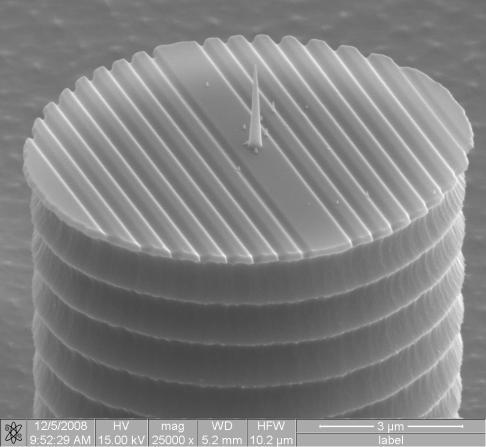
17 15 Fabrication process: pillar growth Electron Beam 5 Kev, 2 nm spot Pt precursor gas gold Si-N Membrane 15 nm 100 nm pillar height 2.5 m pillar base 100 nm Tip radius of curvature nm

 maximum 80 NH")

18 Single QD Raman spectrum 16 Amine peak estimated 10 NH 2 groups (from company linkage data) maximum 80 NH 2 groups De Angelis et al. Nano Lett., 8 (8), (2008)

19 QDs manipulation and deposition on the NW 17

20 Adiabatic cone on PhC 18 Di Fabrizio, E., et al., Italian patent n. TO2008A nm radius Gold and Silver cones


21 AFM-Raman spectroscopy 19 Nanodevice on a cantilever efficiently acting as AFM tip and as a nanontenna for Raman scattering.

22 Optical setup Focal plane on the cantilever Focal plane on the tip end TASC CBM Trieste 20

23 Raman & AFM: chemical sensing 21 Laser lithography Si/SiO2 (optical image) Silicon nanocrystal Cantilever with Nano-Cone 10 m silica SiO x Raman Band Si Raman Band

24 Raman & AFM: chemical sensing, coarse scan 22 Silicon nanocrystal Cantilever with Nano-Cone silica p1 p2 p3 p4 p5 p6 p7 p8 p9 p10 2 m Scan length 2 µm Scan step ~220 nm


25 Raman & AFM: chemical sensing, fine scan Simultaneously: Topography Raman intensity at 520 cm -1 AFM topography Sensing and topography resolution 5-10 nm From Raman detailed line shape analysis we found nano crystal size 5-7 nm 110 nm Fine scan along the wall. AFM scan step: 7 nm 23

26 Selected results 24


27 Nanocone on biological samples Lipid bilayers in liquid: 4 nm thickness. Sharp topography without shear effects. Nanocone performs exceptionally well on biological samples in physiological environment Force spectroscopy on titin protein Topography on insulin fibrils in liquid: down to resolution of protofibrillar structures (3-4 nm). Only 1 report in literature. Titin Pulling 25


28 Recent results:sers on amyloid fibrils (on silicon) Amyloid fibrils are involved in Alzheimer disease. Their characterization by AFM is widely used, however to date there are few reports about their Raman signature. Here we show that insulin fibrils on silicon, bear a Raman signature (1), compared to the background (2). 1 um scan (topography)
29 Adiabatic compression: behind the scenes 27 Strong field SPP Ag laser (visible)
30 Adiabatic compression: behind the scenes 27 Strong field SPP Ag What kind of source? laser (visible)


31 28 The source z x Plane wave X-polarized Radial polarization y z x

32 3D simulation: radial-like source 29 z x 500nm Adiabatic compression Field enhancement ~100 Strong localization

33 3D simulation: longitudinal plane wave X 30 z x 500nm NO Adiabatic compression Phase dependence Field enhancement ~20


34 Summarizing Nmerical simulation Calculation Nature Nanotech. 5, 67 (2010) Radial mode (TM0) benzenethiol Tip radius < 10nm High spatial resolution Adiabatic compression Energy at the nanoscale Opt. Exp. 19, (2011) PRB 86, (2012) Opt. Lett. 37, 545 (2012) 31
35 Outline Planar structures & Photonic crystals Metallic structures & Plasmonics AFM-Raman: toward few/single molecule detection Adiabatic compression in details (not too many though) Detection in Attomolar solution concentration Artificial Lotus effect Computational approach: a very powerful resource Few photons problem Electroporation Modulated SPPERS Adiabatic electrical generation Hot electrons nanoscopy THz antennas Optical computing Opto-mechanics Plasmo-catalysis Thermo-catalysis 32

36 Diffusion limit 33 1 fm analyte concentration


37 Question: can the diffusion limit be avoided? SuperHydrophobicity for analyte concentration 34 Evaporation implies concentration and localization


 Both rigid and flexible")
38 Artificial Lotus effect: micropatterned surface 35 Photolithography combined with Deep RIE Full controllable size High aspect ratio (up to 20 or more) Both rigid and flexible substrates 10 m
39 Artificial Lotus effect 36 Evaporation of 10 ml of water in few minutes


40 36 Artificial Lotus effect Evaporation of 10 ml of water in few minutes Few molecules... and we know where they are!


41 Evaporation and concentration (10 Attomolar) Rhodamine 37
 38 Raman detection of")

 Roughly 10")
42 Intensity (arb. units) 38 Raman detection of Rhodamine on pillars 10 l mol/l Rhodamine 6G Raman shift (cm -1 ) Roughly 10 Rhodamine molecules!


43 Combination of Plasmonics and hydrophobic surfaces m 4 m 200 nm


44 Combination of Plasmonics and hydrophobic surfaces 40 3 m 50 nm


45 Combination of Plasmonics and hydrophobic surfaces 41 m m m m

46 Selected results 42
47 Outline Planar structures & Photonic crystals Metallic structures & Plasmonics AFM-Raman: toward few/single molecule detection Adiabatic compression in details (not too many though) Detection in Attomolar solution concentration Artificial Lotus effect Computational approach: a very powerful resource Few photons problem Electroporation Modulated SPPERS Adiabatic electrical generation Hot electrons nanoscopy THz antennas Optical computing Opto-mechanics Plasmo-catalysis Thermo-catalysis 43
48 #1: Few photons sub-wavelenght transmission =514/530nm d: 30nm-200nm Noise Signal 200nm very high signal to noise ratio ~ 100 field localization European project: FOCUS z=150nm along x (nm) (I hole /I bg ) x ~1400 and (I hole /I bg ) y ~120 Very high signal to-noise ratio! ~E nm nm Z Max E ~1.7V/m Decay of E along z (nm) (side hole) (I hole /I bg ) x ~1400 and (I hole /I bg ) y ~120 Very high signal to-noise ratio! ~E 0 hole Polarization: X Holes diameter: 80nm nm nm ~10nm 1/e 0: 530nm Period: 1 m 44


 x ~1400 and (I hole /I bg ) y")

")


49 #1: Few photons sub-wavelenght transmission =514/530nm d: 30nm-200nm Noise E field travelling through the slab Signal 200nm very high signal to noise ratio ~ 100 field localization z=150nm along x (nm) (I hole /I bg ) x ~1400 and (I hole /I bg ) y ~120 Very high signal to-noise ratio! ~E nm nm Z Max E ~1.7V/m Decay of E along z (nm) (side hole) (I hole /I bg ) x ~1400 and (I hole /I bg ) y ~120 Very high signal to-noise ratio! ~E 0 hole Polarization: X Holes diameter: 80nm nm nm ~10nm 1/e 0: 530nm Period: 1 m 45


50 #2: Computational electroporation 46 = electrode Va Vb Vc
51 #2: Computational electroporation 47 DNA is negatively charged
 Propagating light Folded protein")
 optical")
52 Unfolded protein #3: Modulated SPPERS (Energy/Life) Propagating light Folded protein Adiabatic compression! Localized light Logic ports (1/0 unit) optical computing Near/Far-field Spectroscopy Au 1 m 48


53 #4: Electrically generated energy concentrator Laser approach Electrical approach a) b) Narrow excitation range Hot electrons injection Wide excitation range ~V Not yet possible (maximum frequency: 100 GHz; Visible: 500THz) Electrical contribution: adiabatic compression Magnetic contribution: spectroscopical shift Near-field magnetic probe? Magnetic compression?


54 m AFM #5: Plasmonic hot electrons nanoscopy GaAs: Egap=1.42eV 5 m Hot electrons map and morphology map 500nm =1060nm (1.17eV); P=2.43 m; d=365nm; Tip radius= 25nm Highly efficient photon-tohot electrons conversion (>30%)! (k vector from the cone) 50
 Characteristics of THz: can penetrate inside most dielectric materials that may be opaque to")

55 Diffraction limit: /2 Solution: resonant plasmonic nanoantennas 51 #6: THz antennas (0.1-10THz) Characteristics of THz: can penetrate inside most dielectric materials that may be opaque to visible light has low photon energies that do not cause photoionization in biological tissues Applications of THz: imaging of plastic/ceramic/semiconductors (e.g, quality control) spectroscopy (semiconductors, molecules, DNA, proteins)


56 #7: Optical computing 52 Logic gate: AND T-shape antenna: Fano mode
 Rho = 1217.")
 Poisson_ratio = 0.")
 resolved spectroscopy (quality factor, force")
57 #8: Opto-mechanic interactions at the nanoscale V Rb = 60nm H = 3.5 um T_polymer = 30nm (SU8) Rho = Kg/m 3 (SU8) Young_mod = *10 8 (1/10 SU8) Poisson_ratio = 0.33 Core = 30nm Au Immagine SEM V V da Mario Applications: time (msec) resolved spectroscopy (quality factor, force spectroscopy, sensing) microfluidics optofluidics V V m 53


58 #9: Plasmocatalysis UV e- TiO 2 h + OH - O - 2 O 2 *OH Two main issues: 1) UV light (<5% total) Visible with doping (nitrogen, tungsten, etc.) 2) High e-h recombination rate & low light absorption Resonant plasmonic nanodevices Bayarri et al., Chem. Eng. J. 200, 158 (2012) c) Al J. Mater. Chem., 2008, 18, superhydrophobicity! Nature Nanotech. 247, 8,


59 e.m. field heat source temperature Temperature (K) 55 #10: Localized high temperature catalysis Single gold nanoantenna =1070nm; P=15 W; Waist=1 m; L=500nm; W=25nm 440 Rb K 300 Joule effect: P =J E Conduction heat transfer: P= T S k/d, k air =0.026 Below 1000 C: Ag=961 C - Au=1065 C - Al=595 C Ti=1670 C - Cu=1083 C - Cr=1857 C Pt= 1768 C
60 Thank you!
61 Extra Remo Proietti Zaccaria Istituto Italiano di Tecnologia (IIT)
62 Computational/analytical research flow chart Photonic Crystals Plasmonic structures Fundamentals: symmetry mode in slab cavities Application: SPPERS* Applications: Super-lenses Sub-wavelength sensors Fundamentals: Quasicrystals properties Quasicrystals Application: Quasicrystals fibers Fundamentals: Adiabatic devices Super-long SPP Metallic Photonic Crystals Fundamentals: High Q factor & Low modal volume *Surface Plasmon Polaritons Enhanced Raman Spectroscopy; SMD project Focus project Nanoantenna project E1
63 Computational and analytical instruments E2 RSoft Lumerical CST Comsol Finite Difference Ttime Domain (FDTD) Finite Integrate Technique (FIT) Robust but not versatile Finite Element Method (FEM) Less robust than CST but very versatile Plane wave expansion (PMW) Rigorous Coupled Wave Analysis (RCWA) Finite Difference Time Domain (FDTD) Mathematica Analytical tool


64 Plasmonic at the DUV range (Life/Energy) Extinction eff. Extinction Experiment Simulation Al/Al 2 O 3 nanoparticles array 5.8eV! E near-field Energy (ev) ACS Nano 2013 E3

 Matrix of gold")

65 E4 High temperature catalysis (Env.) Matrix of gold nanoantennas 400nm Localized temperature pattern!


66 KAUST 2013 E5 V V V V V=1 V=0.3V V V V V V V
ADOPT Winter School Merging silicon photonics and plasmonics
 ADOPT Winter School 2014 Merging silicon photonics and plasmonics Prof. Min Qiu Optics and Photonics, Royal Institute of Technology, Sweden and Optical Engineering, Zhejiang University, China Contents
Plasmonics: Application-oriented fabrication. Part 1. Introduction
 Plasmonics: Application-oriented fabrication Part 1. Introduction Victor Ovchinnikov Department of Aalto Nanofab Aalto University Espoo, Finland Alvar Aalto was a famous Finnish architect and designer
Plasmonics using Metal Nanoparticles. Tammy K. Lee and Parama Pal ECE 580 Nano-Electro-Opto-Bio
 Plasmonics using Metal Nanoparticles Tammy K. Lee and Parama Pal ECE 580 Nano-Electro-Opto-Bio April 1, 2007 Motivation Why study plasmonics? Miniaturization of optics and photonics to subwavelength scales
Basics of Plasmonics
 Basics of Plasmonics Min Qiu Laboratory of Photonics and Microwave Engineering School of Information and Communication Technology Royal Institute of Technology (KTH) Electrum 229, 16440 Kista, Sweden http://www.nanophotonics.se/
Nanophotonics: principle and application. Khai Q. Le Lecture 11 Optical biosensors
 Nanophotonics: principle and application Khai Q. Le Lecture 11 Optical biosensors Outline Biosensors: Introduction Optical Biosensors Label-Free Biosensor: Ringresonator Theory Measurements: Bulk sensing
nanosilicon Nanophotonics
 nanosilicon Nanophotonics Lorenzo Pavesi Universita di Trento Italy Outline Silicon Photonics NanoSilicon photonics Silicon Nanophotonics NanoSilicon Nanophotonics Conclusion Outline Silicon Photonics
Satoshi Kawata. Near-Field Optic s and Surface Plasmon Polaritons
 Satoshi Kawata Near-Field Optic s and Surface Plasmon Polaritons Near-Field Optics and the Surface Plasmon Polariton Dieter W. Pohl 1 1. Introduction 1 2. Back to the Roots 1 2.1. Rayleigh and Mie Scattering
Plasmonic Nanostructures II
 Plasmonic Nanostructures II Dr. Krüger / Prof. M. Zacharias, IMTEK, Propagation of SPPs Propagation distance decreases with decreasing strip width! 2 Dr. Krüger / Prof. M. Zacharias, IMTEK, Bound and leaky
Fs- Using Ultrafast Lasers to Add New Functionality to Glass
 An IMI Video Reproduction of Invited Lectures from the 17th University Glass Conference Fs- Using Ultrafast Lasers to Add New Functionality to Glass Denise M. Krol University of California, Davis 17th
Silver Diffusion Bonding and Layer Transfer of Lithium Niobate to Silicon
 Chapter 5 Silver Diffusion Bonding and Layer Transfer of Lithium Niobate to Silicon 5.1 Introduction In this chapter, we discuss a method of metallic bonding between two deposited silver layers. A diffusion
Magnetic Force Microscopy: nanoscale magnetic imaging and lithography
 NTEGRA Aura Magnetic Force Microscopy: nanoscale magnetic imaging and lithography The principle of Magnetic Force Microscopy (MFM) is based on the detection of the interaction between the sample and a
Design Optimization of Structural Parameters for Highly Sensitive Photonic Crystal Label-Free Biosensors
 Sensors 2013, 13, 3232-3241; doi:10.3390/s130303232 Article OPEN ACCESS sensors ISSN 1424-8220 www.mdpi.com/journal/sensors Design Optimization of Structural Parameters for Highly Sensitive Photonic Crystal
Polymer-based optical interconnects using nano-imprint lithography
 Polymer-based optical interconnects using nano-imprint lithography Arjen Boersma,Sjoukje Wiegersma Bert Jan Offrein, Jeroen Duis, Jos Delis, Markus Ortsiefer, Geert van Steenberge, MikkoKarppinen, Alfons
Shape Light Beams. Using Plasmonics to. Federico Capasso, Nanfang Yu, Ertugrul Cubukcu and Elizabeth Smythe
 Using Plasmonics to Shape Light Beams Federico Capasso, Nanfang Yu, Ertugrul Cubukcu and Elizabeth Smythe Plasmonic structures shape semiconductor laser beams. Left: A plasmonic collimator spreads out
Supplementary Figure 1 Scanning electron micrograph (SEM) of a groove-structured silicon substrate. The micropillars are ca. 10 μm wide, 20 μm high
 of a groove-structured silicon substrate. The micropillars are ca. 10 μm wide, 20 μm high") Supplementary Figure 1 Scanning electron micrograph (SEM) of a groove-structured silicon substrate. The micropillars are ca. 10 μm wide, 20 μm high and own the gap of 10 μm. Supplementary Figure 2 Strictly
Supplementary Figure 1 Scanning electron micrograph (SEM) of a groove-structured silicon substrate. The micropillars are ca. 10 μm wide, 20 μm high and own the gap of 10 μm. Supplementary Figure 2 Strictly
Plasmonic Probe With Circular Nano-Moat for far-field Free Nanofocusing
 Zhang and Wang Nanoscale Research Letters (2016) 11:421 DOI 10.1186/s11671-016-1619-y NANO EXPRESS Plasmonic Probe With Circular Nano-Moat for far-field Free Nanofocusing Mingqian Zhang 1* and Tianying
CREOL, The College of Optics & Photonics, University of Central Florida
 Metal Substrate Induced Control of Ag Nanoparticle Plasmon Resonances for Tunable SERS Substrates Pieter G. Kik 1, Amitabh Ghoshal 1, Manuel Marquez 2 and Min Hu 1 1 CREOL, The College of Optics and Photonics,
Phil Saunders, spacechannel.org
 Guidi with Phil Saunders, spacechannel.org ng Light Long-Range nge Plasmons Aloyse Degiron, Pierre Berini and David R. Smith Long-range surface plasmons are optical modes propagating along metallic circuits
Superionic Solid State Stamping (S4)
") Superionic Solid State Stamping (S4) Lead Faculty Researcher: Placid Ferreira Department: Materials Science & Engineering Hsu et al, Nano Letters, 2007 1. Description: This dry, single step, electrochemical
Superionic Solid State Stamping (S4) Lead Faculty Researcher: Placid Ferreira Department: Materials Science & Engineering Hsu et al, Nano Letters, 2007 1. Description: This dry, single step, electrochemical
7-2E. Photonic crystals
 7-2E. Photonic crystals Purdue Univ, Prof. Shalaev, http://cobweb.ecn.purdue.edu/~shalaev/ Univ Central Florida, CREOL, Prof Kik, http://sharepoint.optics.ucf.edu/kik/ose6938i/handouts/forms/allitems.aspx
Multiphoton lithography based 3D micro/nano printing Dr Qin Hu
 Multiphoton lithography based 3D micro/nano printing Dr Qin Hu EPSRC Centre for Innovative Manufacturing in Additive Manufacturing University of Nottingham Multiphoton lithography Also known as direct
PUBLISHED VERSION.
 PUBLISHED VERSION Ruan, Yinlan; Afshar Vahid, Shahraam; Monro, Tanya Mary Efficient excitation of surface plasmons in metal nanorods using large longitudinal component of high index nano fibers, Optics
Solar Cells and Photosensors.
 Designing Photonic Crystals in Strongly Absorbing Material for Applications in Solar Cells and Photosensors. Minda Wagenmaker 1, Ebuka S. Arinze 2, Botong Qiu 2, Susanna M. Thon 2 1 Mechanical Engineering
Engineering in the Optimization of Resolution of Nanohole Arrays in Metal Films for Refractive Index Sensing
 Engineering in the Optimization of Resolution of Nanohole Arrays in Metal Films for Refractive Index Sensing by Gabriela Andrea Cervantes Téllez B.Sc., Instituto Tecnológico de Estudios Superiores de Monterrey,
Light Trapping Enhancement in Thin Film Silicon Solar Cell with Different Back Reflector
 International Journal of Electrical Components and Energy Conversion 2017; 3(5): 83-87 http://www.sciencepublishinggroup.com/j/ijecec doi: 10.11648/j.ijecec.20170305.11 ISSN: 2469-8040 (Print); ISSN: 2469-8059
Surface-Plasmon-Enhanced Third-Order Harmonic Generation of Organic Materials
 Surface-Plasmon-Enhanced Third-Order Harmonic Generation of Organic Materials Fanghui Ren 1, Xiangyu Wang 1, Zhongan Li 2, Jingdong Luo 2, Sei-Hum Jang 2, Alex K-Y Jen 2, Alan X. Wang 1* 1 School of Electrical
During solution evaporation, there are two major competing evaporation-driven effects, coffee ring effect and Marangoni flow.
 Abstract Evaporation driven particle packing has been investigated to reveal interesting patterns at micrometer to millimeter scale. While the microscopic structures of these patterns are well characterized,
High Sensitivity of Phase-based Surface Plasmon Resonance in Nano-cylinder Array
 PIERS ONLINE, VOL. 4, NO. 7, 2008 746 High Sensitivity of Phase-based Surface Plasmon Resonance in Nano-cylinder Array Bing-Hung Chen, Yih-Chau Wang, and Jia-Hung Lin Institute of Electronic Engineering,
High Pressure Chemical Vapor Deposition to make Multimaterial Optical Fibers
 High Pressure Chemical Vapor Deposition to make Multimaterial Optical Fibers Subhasis Chaudhuri *1 1, 2, 3, John V. Badding 1 Department of Chemistry, Pennsylvania State University, University Park, PA
In-Situ Monitoring of Pattern Filling in Nano-Imprint Lithography Using Surface Plasmon Resonance
 Copyright 2011 American Scientific Publishers All rights reserved Printed in the United States of America Journal of Nanoscience and Nanotechnology Vol. 11, 1 6, 2011 In-Situ Monitoring of Pattern Filling
Digital resolution enhancement in surface plasmon microscopy
 Digital resolution enhancement in surface plasmon microscopy I.I. Smolyaninov 1) *, J. Elliott 2), G. Wurtz 2), A.V. Zayats 2), C.C. Davis 1) 1) Department of Electrical and Computer Engineering, University
Amorphous silicon waveguides for microphotonics
 4 Amorphous silicon waveguides for microphotonics Amorphous silicon a-si was made by ion irradiation of crystalline silicon with 1 10 15 Xe ions cm 2 at 77 K in the 1 4 MeV energy range. Thermal relaxation
Lecture 13 Nanophotonics in plasmonics. EECS Winter 2006 Nanophotonics and Nano-scale Fabrication P.C.Ku
 Lecture 13 Nanophotonics in plasmonics EECS 598-002 Winter 2006 Nanophotonics and Nano-scale Fabrication P.C.Ku Schedule for the rest of the semester Introduction to light-matter interaction (1/26): How
Laser Micromachining of Bulk Substrates and Thin Films Celine Bansal
 Laser Micromachining of Bulk Substrates and Thin Films Celine Bansal Oxford Lasers Ltd Moorbrook Park Didcot, Oxfordshire, OX11 7HP Tel: +44 (0) 1235 810088 www.oxfordlasers.com Outline Oxford Lasers Importance
High Power Operation of Cryogenic Yb:YAG. K. F. Wall, B. Pati, and P. F. Moulton Photonics West 2007 San Jose, CA January 23, 2007
 High Power Operation of Cryogenic Yb:YAG K. F. Wall, B. Pati, and P. F. Moulton Photonics West 2007 San Jose, CA January 23, 2007 Outline Early work on cryogenic lasers MPS laser technology Recent program
Chapter 3 Silicon Device Fabrication Technology
 Chapter 3 Silicon Device Fabrication Technology Over 10 15 transistors (or 100,000 for every person in the world) are manufactured every year. VLSI (Very Large Scale Integration) ULSI (Ultra Large Scale
Aligned Carbon Nanofibre-Polymer Composite Membranes. CNT Growth and Manipulation. Eleanor Campbell Dept. of Physics, Göteborg University
 Aligned Carbon Nanofibre-Polymer Composite Membranes CNT Growth and Manipulation Eleanor Campbell Dept. of Physics, Göteborg University Plasma CVD Growth Polymer/Nanofibre Composite Low ambient temperature
Modification of Glass by FS Laser for Optical/Memory Applications
 Modification of Glass by FS Laser for Optical/Memory Applications Kazuyuki Hirao and Kiyotaka Miura Department of Material Chemistry Kyoto University International Workshop on Scientific Challenges of
How grooves reflect and confine surface plasmon polaritons
 How grooves reflect and confine surface plasmon polaritons Martin Kuttge, 1,* F. Javier García de Abajo, 2 and Albert Polman 1 1 Center for Nanophotonics, FOM-Institute AMOLF, Sciencepark 113, 1098 XG
Surface Plasmon Effects in Nano-Optics. Greg Gbur Department of Physics and Optical Science, UNC Charlotte, Charlotte, North Carolina 28227
 Surface Plasmon Effects in Nano-Optics Greg Gbur Department of Physics and Optical Science, UNC Charlotte, Charlotte, North Carolina 28227 Shanghai, Jan 2007 Summary Introduction: What is a surface plasmon?
Nanoimprinting in Polymers and Applications in Cell Studies. Albert F. YEE Chemical Engineering & Materials Science UC Irvine
 Nanoimprinting in Polymers and Applications in Cell Studies Albert F. YEE Chemical Engineering & Materials Science UC Irvine Presentation outline Motivation Reversal imprinting Soft inkpad imprinting on
Trench Structure Improvement of Thermo-Optic Waveguides
 International Journal of Applied Science and Engineering 2007. 5, 1: 1-5 Trench Structure Improvement of Thermo-Optic Waveguides Fang-Lin Chao * Chaoyang University of Technology, Wufong, Taichung County
Surface Characterization of Laser Polished Indirect-SLS Parts
 Surface Characterization of Laser Polished Indirect-SLS Parts Jorge A. Ramos, David L. Bourell, Joseph J. Beaman Laboratory for Freeform Fabrication The University of Texas at Austin, Austin, Texas 78712
Supporting Information
 Supporting Information Colloidal Monolayer β-in 2 Se 3 Nanosheets with High Photoresponsivity Guilherme Almeida,&, Sedat Dogan, Giovanni Bertoni,, Cinzia Giannini, Roberto Gaspari,, Stefano Perissinotto,
Mater. Res. Soc. Symp. Proc. Vol Materials Research Society
 Mater. Res. Soc. Symp. Proc. Vol. 940 2006 Materials Research Society 0940-P13-12 A Novel Fabrication Technique for Developing Metal Nanodroplet Arrays Christopher Edgar, Chad Johns, and M. Saif Islam
Optical Observation - Hyperspectral Characterization of Nano-scale Materials In-situ
 Optical Observation - Hyperspectral Characterization of Nano-scale Materials In-situ Research at the nanoscale is more effective, when research teams can quickly and easily observe and characterize a wide
PLASMONICS: RECENT DEVELOPMENTS AND MAIN APPLICATIONS
 PLASMONICS: RECENT DEVELOPMENTS AND MAIN APPLICATIONS Alexandra Boltasseva Department of Photonics Engineering Technical University of Denmark Many thanks to Mark Brongersma (Stanford) Sergey Bozhevolnyi
Trends for Glass in Electrical Components and Systems
 Trends for Glass in Electrical Components and Systems Mike Lanagan Materials Research Institute Penn State University Presented to the International Materials April 15, 2007 Components and Systems Multilayer
PeakForce Tapping and ScanAsyst An introduction to the technique featuring Bruker s Dimension Edge. Bede Pittenger, Ph.D.
 PeakForce Tapping and ScanAsyst An introduction to the technique featuring Bruker s Dimension Edge Bede Pittenger, Ph.D. Dimension Edge with ScanAsyst: High performance AFM breaking down cost and productivity
Lecture 5. SOI Micromachining. SOI MUMPs. SOI Micromachining. Silicon-on-Insulator Microstructures. Agenda:
 EEL6935 Advanced MEMS (Spring 2005) Instructor: Dr. Huikai Xie SOI Micromachining Agenda: SOI Micromachining SOI MUMPs Multi-level structures Lecture 5 Silicon-on-Insulator Microstructures Single-crystal
SUPPLEMENTARY INFORMATION
 Grains and grain boundaries in highly crystalline monolayer molybdenum disulphide Supplementary Figure S1: Commonly-observed shapes in MoS 2 CVD. Optical micrographs of various CVD MoS2 crystal shapes
What s Hot in Heat Assisted Magnetic Recording (HAMR)
") What s Hot in Heat Assisted Magnetic Recording (HAMR) Mark Re Senior Vice President Seagate Research Some of this work was performed as part of the Information Storage Industry Consortium (INSIC) program
What s Hot in Heat Assisted Magnetic Recording (HAMR) Mark Re Senior Vice President Seagate Research Some of this work was performed as part of the Information Storage Industry Consortium (INSIC) program
Efficient, broadband and compact metal grating couplers for silicon-on-insulator waveguides
 Efficient, broadband and compact metal grating couplers for silicon-on-insulator waveguides Stijn Scheerlinck, Jonathan Schrauwen, Frederik Van Laere, Dirk Taillaert, Dries Van Thourhout and Roel Baets
Towards scalable fabrication of high efficiency polymer solar cells
 Towards scalable fabrication of high efficiency polymer solar cells Hui Joon Park 2*, Myung-Gyu Kang 1**, Se Hyun Ahn 3, Moon Kyu Kang 1, and L. Jay Guo 1,2,3 1 Department of Electrical Engineering and
OMICS Group signed an agreement with more than International Societies to make healthcare informati on Open Access. OMICS Group Conferences
 About Omics Group OMICS Group International through its Open Ac cess Initiative is committed to make genuine an d reliable contributions to the scientific commu nity. OMICS Group hosts over 400 leading-edg
3. Overview of Microfabrication Techniques
 3. Overview of Microfabrication Techniques The Si revolution First Transistor Bell Labs (1947) Si integrated circuits Texas Instruments (~1960) Modern ICs More? Check out: http://www.pbs.org/transistor/background1/events/miraclemo.html
Photonic integrated circuits in biochemical food analysis
 Photonic integrated circuits in biochemical food analysis What is Photonics? Page 2 Photonics is the physical science of light generation, detection, and manipulation through e.g. transmission, modulation,
for New Energy Materials and Devices; Beijing National Laboratory for Condense Matter Physics,
 Electronic Supplementary Information Highly efficient core shell CuInS 2 /Mn doped CdS quantum dots sensitized solar cells Jianheng Luo, a Huiyun Wei, a Qingli Huang, a Xing Hu, a Haofei Zhao, b Richeng
Development of photonic and thermodynamic crystals conforming to sustainability conscious materials tectonics
 Sustainable Chemistry 103 Development of photonic and thermodynamic crystals conforming to sustainability conscious materials tectonics S. Kirihara, N. Ohta, T. Niki, Y. Uehara & S. Tasaki Joining and
Structure and optical properties of M/ZnO (M=Au, Cu, Pt) nanocomposites
 nanocomposites") Solar Energy Materials & Solar Cells 8 () 339 38 Structure and optical properties of M/ (M=Au, Cu, Pt) nanocomposites U. Pal a,b, *, J. Garc!ıa-Serrano a, G. Casarrubias-Segura a, N. Koshizaki c, T. Sasaki
Solar Energy Materials & Solar Cells 8 () 339 38 Structure and optical properties of M/ (M=Au, Cu, Pt) nanocomposites U. Pal a,b, *, J. Garc!ıa-Serrano a, G. Casarrubias-Segura a, N. Koshizaki c, T. Sasaki
Virtual Prototyping of a Microwave Fin Line Power Spatial Combiner Amplifier
 Virtual Prototyping of a Microwave Fin Line Power Spatial Combiner Amplifier Alberto Leggieri, Franco Di Paolo, Davide Passi Department of Electronic Engineering University of Roma Tor Vergata 00133 Roma
FABRICATION AND CHARACTERIZATION OF QUANTUM-WELL AND QUANTUM-DOT METAL CAVITY SURFACE-EMITTING NANOLASERS
 FABRICATION AND CHARACTERIZATION OF QUANTUM-WELL AND QUANTUM-DOT METAL CAVITY SURFACE-EMITTING NANOLASERS By Eric Wei Senior Thesis in Electrical Engineering University of Illinois at Urbana-Champaign
JSM-7800F Field Emission Scanning Electron Microscope
 JSM-7800F catalogue JSM-7800F Field Emission Scanning Electron Microscope We provide high performance The Ultimate Research Tool for Multi-Disciplinary Research Institutions Extreme resolution The super
Efficient organic distributed feedback lasers with active films imprinted by thermal nanoimprint lithography
 Efficient organic distributed feedback lasers with active films imprinted by thermal nanoimprint lithography bidali zenuenean, ondo dago. Efficient organic distributed feedback lasers with active films
Nanotechnology for Molecular and Cellular Manipulation
 Nanotechnology for Molecular and Cellular Manipulation Logan Liu Micro and Nano Technology Lab Department of Electrical & Computer Engineering University of Illinois Physical Systems Nano vs. Bio Micro
Optical Control of Surface Plasmon Coupling in Organic Light Emitting Devices with Nanosized Multi-cathode Structure
 Proceedings of the 5 th International Conference on Nanotechnology: Fundamentals and Applications Prague, Czech Republic, August 11-13, 2014 Paper No. 234 Optical Control of Coupling in Organic Light Emitting
THIN FILM THICKNESS MEASUREMENT FOR EVALUATION OF RESIDUAL LAYER OF NANO-IMPRINT LITHOGRAPHY USING NEAR-FIELD OPTICS
 9 th INTERNATIONAL SYMPOSIUM ON MEASUREMENT AND QUALITY CONTROL (9 th ISMQC) November 21 24, 27, IIT Madras THIN FILM THICKNESS MEASUREMENT FOR EVALUATION OF RESIDUAL LAYER OF NANO-IMPRINT LITHOGRAPHY
Characterization of Materials with a Combined AFM/Raman Microscope
 Characterization of Materials with a Combined AFM/Raman Microscope Marko Surtchev 1, Sergei Magonov 1 and Mark Wall 2 1 NT-MDT America, Tempe, AZ U.S.A. 2 Thermo Fisher Scientific, Madison, WI, U.S.A.
RIE lag in diffractive optical element etching
 Microelectronic Engineering 54 (2000) 315 322 www.elsevier.nl/ locate/ mee RIE lag in diffractive optical element etching Jyh-Hua Ting *, Jung-Chieh Su, Shyang Su a, b a,c a National Nano Device Laboratories,
DIRECT NANO-PATTERNING WITH NANO-OPTIC DEVICES
 DIRECT NANO-PATTERNING WITH NANO-OPTIC DEVICES A Thesis by VIJAY MEENASHI SUNDARAM Submitted to the Office of Graduate Studies of Texas A&M University in partial fulfillment of the requirements for the
AFM-Raman Characterization of Pharmaceutical Tablets
 AFM-Raman Characterization of Pharmaceutical Tablets Compound Distribution Studies in Pharmaceutical Tablets by Integrated AFM-Raman Instrument 1,2 1 Sergey Shashkov and Pavel Dorozhkin, 1 NT-MDT Co.,
Materials Characterization for Stress Management
 Materials Characterization for Stress Management Ehrenfried Zschech, Fraunhofer IZFP Dresden, Germany Workshop on Stress Management for 3D ICs using TSVs San Francisco/CA, July 13, 2010 Outline Stress
FY06 ACCOMPLISHMENTS. Nanoelectronics Manufacture, Inspection, and Repair using Thermal Dip Pen Nanolithography
 FY06 ACCOMPLISHMENTS Nanoelectronics Manufacture, Inspection, and Repair using Thermal Dip Pen Nanolithography William P. King Georiga Institute of Technology FY06 was the second year of this grant, and
2.1 µm CW Raman Laser in GeO 2 Fiber
 2.1 µm CW Raman Laser in GeO 2 Fiber B. A. Cumberland, S. V. Popov and J. R. Taylor Femtosecond Optics Group, Imperial College London, SW7 2AZ, United Kingdom O. I. Medvedkov, S. A. Vasiliev, E. M. Dianov
3.46 OPTICAL AND OPTOELECTRONIC MATERIALS
 Badgap Engineering: Precise Control of Emission Wavelength Wavelength Division Multiplexing Fiber Transmission Window Optical Amplification Spectrum Design and Fabrication of emitters and detectors Composition
FANO PLASMONICS MADE SIMPLE
 Higher-order resonances in single-arm nanoantennas: Evidence of Fano-like interference FANO PLASMONICS MADE SIMPLE F. López-Tejeira, R. Paniagua-Domínguez, R. Rodríguez-Oliveros José A. Sánchez-Gil, Instituto
Qswitched lasers are gaining more interest because of their ability for various applications in remote sensing, environmental monitoring, micro
 90 Qswitched lasers are gaining more interest because of their ability for various applications in remote sensing, environmental monitoring, micro machining, nonlinear frequency generation, laserinduced
Surface plasmon enhanced emission from dye doped polymer layers
 Surface plasmon enhanced emission from dye doped polymer layers Terrell D. Neal, a) Koichi Okamoto, and Axel Scherer Department of Electrical Engineering, California Institute of Technology, Pasadena,
Surface Plasmon Resonance Analyzer
 Surface Plasmon Resonance Analyzer 5 6 SPR System Based on Microfluidics Wide Dynamic Range Kinetic Analysis by Detection of Association /Dissociation of Bio-Molecules Measuring of Mass Change below
Structural and Optical Properties of MnO 2 : Pb Nanocrystalline Thin Films Deposited By Chemical Spray Pyrolysis
 IOSR Journal of Engineering (IOSRJEN) e-issn: 2250-3021, p-issn: 2278-8719 Vol. 3, Issue 4 (April. 2013), V4 PP 52-57 Structural and Optical Properties of MnO 2 : Pb Nanocrystalline Thin Films Deposited
International Journal of Scientific & Engineering Research, Volume 6, Issue 2, February-2015 ISSN PHOTONIC CRYSTAL FIBER- AN OVERVIEW
 45 PHOTONIC CRYSTAL FIBER- AN OVERVIEW Neha Mahnot1, Shikha Maheshwary2, Rekha Mehra3 1, 2, 3 Govt. Engg. College, Ajmer 2 shikhasm1992@gmail.com 1 neha29mahnot@gmail.com Abstract- This review paper gives
average diameter = 3 nm, from PlasmaChem) was mixed in NLCs to produce QDembedded
 was mixed in NLCs to produce QDembedded") Electronic Supplementary Material (ESI) for RSC Advances. This journal is The Royal Society of Chemistry 2014 Supporting information Experimental Section The blended CLC-monomer materials used to fabricate
Electronic Supplementary Material (ESI) for RSC Advances. This journal is The Royal Society of Chemistry 2014 Supporting information Experimental Section The blended CLC-monomer materials used to fabricate
Directional Surface Plasmon Coupled Emission
 Journal of Fluorescence, Vol. 14, No. 1, January 2004 ( 2004) Fluorescence News Directional Surface Plasmon Coupled Emission KEY WORDS: Surface plasmon coupled emission; high sensitivity detection; reduced
Application Note #124 VITA: Quantitative Nanoscale Characterization and Unambiguous Material Identification for Polymers
 Local thermal analysis identifies polymer AFM image of polymer blend Application Note #124 VITA: Quantitative Nanoscale Characterization and Unambiguous Material Identification for Polymers VITA module
2009 Department of Physics and Astronomy Georgia State University Atlanta, GA US Israel Binational Science Foundation
 p.1 Photo Credit: I. Tsukerman, Seefeld, Austria, January, 2009 US Israel Binational Science Foundation Nanoplasmonics: The Physics behind the Applications Mark I. Stockman,, Atlanta, GA 30303, USA p.2
Surface-plasmon wavefront and spectral shaping by near-field holography
 LASER & PHOTONICS REVIEWS Laser Photonics Rev. 10, No. 3, 360 381 (2016) / DOI 10.1002/lpor.201500242 Abstract Surface-plasmon-polariton waves are twodimensional electromagnetic surface waves that propagate
Free standing Multilayer Thin Film of Cellulose Nanocrystals
 Free standing Multilayer Thin Film of Cellulose Nanocrystals Chaoyang Jiang Department of Chemistry The University of South Dakota Edmonton, June 25, 2009 Cellulose Nanocrystals Nanotechnology R&D Priority
Symmetric hybrid surface plasmon polariton waveguides for 3D photonic integration
 Symmetric hybrid surface plasmon polariton waveguides for 3D photonic integration Yusheng Bian, 1 Zheng Zheng, 1,* Xin Zhao, 1 Jinsong Zhu, 2 and Tao Zhou 3 1 School of Electronic and Information Engineering,
Growth and Doping of SiC-Thin Films on Low-Stress, Amorphous Si 3 N 4 /Si Substrates for Robust Microelectromechanical Systems Applications
 Journal of ELECTRONIC MATERIALS, Vol. 31, No. 5, 2002 Special Issue Paper Growth and Doping of SiC-Thin Films on Low-Stress, Amorphous Si 3 N 4 /Si Substrates for Robust Microelectromechanical Systems
EECS130 Integrated Circuit Devices
 EECS130 Integrated Circuit Devices Professor Ali Javey 9/13/2007 Fabrication Technology Lecture 1 Silicon Device Fabrication Technology Over 10 15 transistors (or 100,000 for every person in the world)
Plastic Coated Silica/Silica (Low OH) FIBER CROSS SECTION Polyimide and Acrylate Coated. Nylon and Tefzel Coated
 FIBER CROSS SECTION Polyimide and Acrylate Coated. Nylon and Tefzel Coated") DESCRIPTION When looking for a high quality fiber with superior transmission and a numerical aperture (N.A.) of 0.22 for efficient light coupling, the is the fiber of choice. The Anhydroguide fiber is
DESCRIPTION When looking for a high quality fiber with superior transmission and a numerical aperture (N.A.) of 0.22 for efficient light coupling, the is the fiber of choice. The Anhydroguide fiber is
Self-Assembled Nanocrystals Through Change in. Nanocrystallinity
 Supporting informations Modulating Physical Properties of Isolated and Self-Assembled Nanocrystals Through Change in Nanocrystallinity Nicolas Goubet,, Cong Yan,, Dario Polli, Hervé Portalès,, Imad Arfaoui,,
TEM imaging and diffraction examples
 TEM imaging and diffraction examples Duncan Alexander EPFL-CIME 1 Diffraction examples Kikuchi diffraction Epitaxial relationships Polycrystalline samples Amorphous materials Contents Convergent beam electron
Challenges and Future Directions of Laser Fuse Processing in Memory Repair
 Challenges and Future Directions of Laser Fuse Processing in Memory Repair Bo Gu, * T. Coughlin, B. Maxwell, J. Griffiths, J. Lee, J. Cordingley, S. Johnson, E. Karagiannis, J. Ehrmann GSI Lumonics, Inc.
Supplementary Figure S1 Crystal structure of the conducting filaments in sputtered SiO 2
 Supplementary Figure S1 Crystal structure of the conducting filaments in sputtered SiO 2 based devices. (a) TEM image of the conducting filament in a SiO 2 based memory device used for SAED analysis. (b)
Lateral epitaxial growth of two-dimensional layered semiconductor heterojunctions
 Lateral epitaxial growth of two-dimensional layered semiconductor heterojunctions Xidong Duan, Chen Wang, Jonathan Shaw, Rui Cheng, Yu Chen, Honglai Li, Xueping Wu, Ying Tang, Qinling Zhang, Anlian Pan,
PRECISION OPTICAL FILTERS BY EOSS - ENHANCED OPTICAL SPUTTERING SYSTEM. Fraunhofer
 PRECISION OPTICAL FILTERS BY EOSS - ENHANCED OPTICAL SPUTTERING SYSTEM EOSS ENHANCED OPTICAL SPUTTERING SYSTEM Fraunhofer IST, Braunschweig Contact: Dr. M. Vergöhl +49 531 2155 640 EOSS Coating System
Micro Laser Assisted Machining (µ-lam) of Semiconductors and Ceramics. Machining Direction
 of Semiconductors and Ceramics. Machining Direction") Micro Laser Assisted Machining (µ-lam) of Semiconductors and Ceramics John Patten, Director, Manufacturing Research Center Western Michigan University Machining Direction IR laser Machining Direction Work
Micro Laser Assisted Machining (µ-lam) of Semiconductors and Ceramics John Patten, Director, Manufacturing Research Center Western Michigan University Machining Direction IR laser Machining Direction Work
Low-Loss Grating-Coupled Silicon Ridge Waveguides and Ring Resonators for Optical Gain at Telecommunication Frequencies
 Low-Loss Grating-Coupled Silicon Ridge Waveguides and Ring Resonators for Optical Gain at Telecommunication Frequencies J. P. Balthasar Müller Science Institute, University of Iceland, Dunhaga 3, IS-107
NRL Institute for Nanoscience 1 May 2012
 NRL Institute for Nanoscience 1 May 2012 Dr. Eric S. Snow, Director The Naval Research Laboratory Highly interdisciplinary laboratory Research Focus Areas Battlespace Environments, Undersea Warfare, Space