Henkel Electronic Solutions
|
|
|
- Flora Dean
- 6 years ago
- Views:
Transcription


1 Henkel Electronic Solutions

2 WORLDWIDE MANUFACTURING & ORGANIZATION ELECTRONICS GROUP OF HENKEL City of Industry, California Olean, New York Dublin, Ireland Hemel Hempstead, UK Yantai,China Isogo, Japan Tainan, Taiwan Irvine, California Lianyungang, China Ecatepec de Morelos, Mexico Ipoh, Malaysia Sao Paulo, Brazil Kuala Lumpur, Malaysia Headquarters/Product Development Product Development/Manufacturing Product Development Manufacturing Across the Board, Around the Globe. Corporate Profile Henkel Corporation Henkel is the world s leading and most progressive provider of qualified, compatible material sets for semiconductor packaging, printed circuit board (PCB) assembly and advanced soldering solutions. As the only materials developer and formulator with vast technical expertise for all materials required for package production and assembly, Henkel is uniquely positioned to deliver world-class materials products, process expertise and total solutions across the board to enable tomorrow s electronic industry.
.... 14 System-in-Package (SiP)....................... 18 Flash Memory................................ 21 Semiconductor Materials Hysol Die Attach Adhesives.")

3 CONTENTS Semiconductor Market Solutions Discrete Components Quad Flat Pack (QFP) Quad Flat No-Lead (QFN) Ball Grid Array/Chip Scale Package (BGA/CSP) System-in-Package (SiP) Flash Memory Semiconductor Materials Hysol Die Attach Adhesives Hysol Semiconductor Underfills Hysol Semiconductor Encapsulants Hysol Thermal Compression Materials Hysol Coating Powders Hysol Electronic Molding Compounds Hysol and Hysol Huawei Semiconductor Molding Compounds Multicore Accurus Solder Spheres Printed Circuit Board (PCB) Assembly Materials Multicore Solder Paste Multicore Fluxes Multicore Cored Wire Multicore Solder Accessories Chip on Board Encapsulant Materials Loctite Board Level Underfills Loctite Thermal Management Materials Loctite Electrically Conductive Adhesives Loctite Chipbonder Surface Mount Adhesives Circuit Board Protection Solutions Flat Panel Display Materials Flat Panel Display Solutions Semiconductor Solutions Solutions Across the Board Periodic Table of Elements

4 MATERIAL SOLUTIONS FOR ELECTRONIC PACKAGING AND ASSEMBLY SEMICONDUCTOR Die Attach Adhesives Semiconductor Underfills Semiconductor Encapsulants Thermal Compression Materials Coating Powders Electronic Molding Compounds Semiconductor Molding Compounds Solder and Flux Materials 2


5 PCB ASSEMBLY FLAT PANEL DISPLAY Solder and Flux Materials Chip on Board Encapsulant Materials Board Level Underfills Thermal Management Materials Electrically Conductive Adhesives Surface Mount Adhesives Circuit Board Protection Solutions Adhesives Cleaners, Developers and Strippers 3
6 SEMICONDUCTOR MARKET SOLUTIONS Across the Board, Around the Globe. 4
 QMI536HT GR2310 GR15F-A KL1000-3LX KO1095 QMI547 GR2710 GR15F-1 KL1000-4T QMI168 GR2811 GR360A-F8 KL2500-1K QMI519 MG40FS GR750 KL4500-1 QMI529HT KLG200 KL5000-HT QMI529NB")
7 SEMICONDUCTOR MARKET SOLUTIONS DISCRETE COMPONENTS Discrete Components Die Attach Adhesives Electronic Molding Compounds Encapsulants Molding Compounds Conductive Non-Conductive GR2220 FP0087 Green Non-Green DA100 (Solder) QMI536HT GR2310 GR15F-A KL1000-3LX KO1095 QMI547 GR2710 GR15F-1 KL1000-4T QMI168 GR2811 GR360A-F8 KL2500-1K QMI519 MG40FS GR750 KL QMI529HT KLG200 KL5000-HT QMI529NB MG15F-0140 MG21F-02 MG35F MG45F-0459LS MG40F DIE ATTACH ADHESIVES: CONDUCTIVE FINISH (Cu, Ag, Au) MRT ELECTRICAL CONDUCTIVITY DISPENSABILITY CURE SCHEDULE THERMAL CONDUCTIVITY, W/mk KO1095 Epoxy-based die attach paste Cu L x 10-3 Very Good C (Oven) 2.1 QMI168 Similar properties to QMI519, manufactured in our Yantai plant. Ag, Au L x 10-4 Good C C (Oven) 3.8 QMI519 JEDEC L1 260 C for SOIC, industry standard for QFN packages. Industry standard for preplated finishes. Exceptional performance on clean uncoated silver-plated finishes. High adhesion, excellent electrical and thermal performance. Ag, Au L x 10-4 Very Good C then C (Oven) 3.8 QMI529HT For component or die attach where very high electrical and thermal conductivity is required. Suitable for high heat dissipation devices and solder replacement applications. Ag, Au L x 10-5 Fair C C (Oven) 7.0 QMI529NB No bleed version of QMI519 for use on NiPdAu, and alloy 42 applications. Ag, Au L x 10-4 Good C (Oven) 3.8 5
8 SEMICONDUCTOR MARKET SOLUTIONS DISCRETE COMPONENTS DIE ATTACH: CONDUCTIVE SOLDER APPLICATION VISCOSITY, cps ALLOY REFLOW CLEANABILITY VOID LEVELS IPC/J-STD-004 CLASSIFICATION DA100 (Solder) Flux designed for solder die attach paste applications Dispensing 250,000 High Pb Forming Gas Excellent Very Low ROL0 DIE ATTACH ADHESIVES: NON-CONDUCTIVE FINISH (Cu, Ag, Au) MRT ELECTRICAL CONDUCTIVITY DISPENSABILITY CURE SCHEDULE THERMAL CONDUCTIVITY, W/mk QMI536HT High thermal version of QMI536, ideal for mixed stacked die applications. Non-die damaging filler. Ag, Au L x Excellent C C (Oven) 0.9 QMI547 Non-conductive paste for leadframe applications Au, Ag, Cu L x Excellent C C (Oven) 0.3 ELECTRONIC MOLDING COMPOUNDS CONVENTIONAL MOLD SPIRAL FLOW 177 C CTEa2, CURE 177 C FLEXURAL STRENGTH, psi FLEXURAL MODULUS, psi LASER MARKABLE GR2220 Black / conventional molding of MnO caps conv sec 18, x 10 6 N GR2310 GR2710 Gold / non-halogenated molding powder, tantalum and ceramic capacitors, leaded or surface-mounted sensors. Gold / low stress/non-flame retarded molding powder, tantalum and ceramic capacitors, leaded or surfacemounted sensors. Auto/conv sec 20, x 10 6 Y Auto/conv sec 19, x 10 6 Y GR2811 Gold / thin wall-crack resistant, low stress, fast cycle time Auto/conv sec 20, x 10 6 Y MG40FS Black / conventional molding of SMD and SIP networks. Gold version MG40F-0526 available. conv sec 19, x 10 6 N ENCAPSULANTS RECOMMENDED CURE FLOW SPEED VISCOSITY 25 C, cps % FILLER FP0087 Low stress fill for potting automated sensor and diodes, high Tg C C High 20,


9 SEMICONDUCTOR MARKET SOLUTIONS MOLDING COMPOUNDS: GREEN DISCRETE COMPONENTS VOLTAGE RATING IONIC PERMITIVITY, ROOM TEMP IONIC PERMITIVITY, 150 C MSL GREEN SPIRAL FLOW, CM GR15F-A Very high Tg, low stress, green semiconductor grade epoxy molding compound designed specifically for high voltage applications. It also boasts superior performance for high temperature power applications due to its high Tg and use of advanced Sigma Technology. > 900V discrete, > 400V IC L1/260 C Y GR15F-1 Green anhydride cured molding compound contains spherical filler and is designed for high voltage applications. This product has excellent moldability performance with high yield rates. > 900V discrete, > 400V IC L1/235 C Y THERMAL CONDUCTIVITY, W/mk GREEN SPIRAL FLOW, cm HOT PLATE GEL TIME, SEC FILLER TYPE GR750 GR750 has alumina fillers and delivers a high thermal conductive solution for TO-220F/3PF's thermal requirements. GR750 's low moisture absorption and low thermal expansion is suitable for stress sensitive devices. GR750 is a green solution. 2.1W/m.K Y Alumina/ Crystalline THERMAL CONDUCTIVITY, W/mk MSL GREEN SPIRAL FLOW, cm HOT PLATE GEL TIME, SEC FILLER TYPE GR360A-F8 Green mold compound with 1/8" flammability rating suitable for bridge, axial and TO packages. GR360A-F8 offers good moldability with lowest cost of ownership. 0.9W/m.K L3/260 C Y Fused KLG200 Green mold compound with 1/4" flammability rating suitable for bridge, axial and TO packages. KLG200 offers superior moldability with lowest cost of ownership. 0.9W/m.K L3/260 C Y Crystalline/ Fused
10 SEMICONDUCTOR MARKET SOLUTIONS DISCRETE COMPONENTS MOLDING COMPOUNDS: NON-GREEN THERMAL CONDUCTIVITY, W/mk MSL GREEN SPIRAL FLOW, cm HOT PLATE GEL TIME, SEC FILLER TYPE KL1000-3LX Provides the lowest cost of ownership with superior moldability and reliability. KL1000-3LX is extremely suitable for bridge, axial and TO packages. 1.3W/m.K L4/220 C N Crystalline KL1000-4T Provides the lowest cost of ownership with superior moldability and reliability. KL1000-4T is extremely suitable for DIP packages. 1.3W/m.K L4/220 C N Crystalline KL2500-1K Low stress molding compound and is suitable for TO and DIP packages and provides superior moldability and reliability 0.9W/m.K L3/260 C N Fused KL High Tg, low stress and high purity characteristics enables packaging of high reliability devices in TO, DIP and SOP format. Its low viscosity properties enable low wire sweep. 0.9W/m.K L1/260 C N Fused THERMAL CONDUCTIVITY, W/mk GREEN SPIRAL FLOW, cm HOT PLATE GEL TIME, SEC FILLER TYPE KL5000-HT Has alumina fillers and delivers a high thermal conductive solution for TO-220F/3PF's thermal requirements. KL5000-HT's low moisture absorption and low thermal expansion is suitable for stress sensitive devices. 2.1W/m.K N Alumina/ Crystalline MG35F Suitable for discrete semiconductors requiring improvement in heat dissipation. MG35F provides high productivity for power transistors. 1.3W/m.K N Crystalline MG45F- 0459LS Has alumina fillers and delivers a high thermal conductive solution for TO-220F/3PF's thermal requirements. MG45F-0459LS 's low moisture absorption and low thermal expansion is suitable for stress sensitive devices. 2.1W/m.K N Alumina/ Crystalline VOLTAGE RATING IONIC PERMITIVITY, ROOM TEMP IONIC PERMITIVITY, 150 C MSL GREEN SPIRAL FLOW, cm MG15F An anhydride cured molding compound designed specifically for use in high voltage power applications requiring good electrical stability at high temperature. This material is specifically recommended for Power Discrete, High Voltage Rectifier and other applications where up until now only silicone molding compounds have been satisfactory. > 900V discrete, > 400V IC L1/235 C N MG21F-02 ECN base molding compound suitable for medium voltage applications. MG21F-02 has excellent moldability on bridge and axial packages. > 700V discrete, > 200V IC L1/235 C N SURFACE FINISH MSL GREEN MAX FILLER SIZE, µm SPIRAL FLOW, cm MG40F High productivity molding compound for high volume encapsulation of SOT and DIP. Ag, Cu L1/260 C N
 MRT ELECTRICAL CONDUCTIVITY DISPENSABILITY CURE SCHEDULE THERMAL CONDUCTIVITY, W/mk KO1095")
 2.")
11 SEMICONDUCTOR MARKET SOLUTIONS QFP QFP Die Attach Adhesives Molding Compounds Conductive Non-Conductive Green Non-Green KO1095 QMI529HT QMI536HT GR828D KL6500H QMI505MT QMI529NB QMI547 KLG650H KL7000HA QMI506 QMI718 KLG730 KL8500 QMI518 QMI519 DIE ATTACH ADHESIVES: CONDUCTIVE FINISH (Cu, Ag, Au) MRT ELECTRICAL CONDUCTIVITY DISPENSABILITY CURE SCHEDULE THERMAL CONDUCTIVITY, W/mk KO1095 Epoxy-based die attach paste Cu L x 10-3 Good C (Oven) 2.1 QMI505MT Lower stress BMI based paste for preplated, alloy 42 and black oxide finishes Au L x 10-3 Good C C (Oven) 2.4 QMI506 Low stress conductive die attach paste for QFPs and TSOPs Au L Good QMI518 Very low stress conductive die attach Ag, Au L Good C C (Oven) C C (Oven) QMI519 JEDEC L1 260 C for SOIC, industry standard for QFN packages. Industry standard for preplated finishes. Exceptional performance on clean uncoated silver-plated finishes. High adhesion, excellent electrical and thermal performance. Ag, Au L x 10-4 Good C C (Oven) 3.8 QMI529HT For component or die attach where very high electrical and thermal conductivity is required. Suitable for high heat dissipation devices and solder replacement applications. Ag, Au L x 10-5 Fair C C (Oven) 7 QMI529NB No bleed version of QMI519 for use on NiPdAu, and alloy 42 applications Ag, Au L x 10-4 Good C (Oven) 3.8 QMI718 Designed to deliver exceptional JEDEC performance in SOIC packages using copper finished leadframes. Cu L x 10-3 Fair C (Oven) 2.7 9
 0.")
12 SEMICONDUCTOR MARKET SOLUTIONS QFP DIE ATTACH: NON-CONDUCTIVE FINISH (Cu, Ag, Au) MRT ELECTRICAL CONDUCTIVITY DISPENSABILITY CURE SCHEDULE THERMAL CONDUCTIVITY, W/mk QMI536HT High thermal version of QMI536, ideal for mixed stacked die applications. Non-die damaging filler. Ag, Au L x Excellent C C (Oven) 0.9 QMI547 Non-conductive paste for leadframe applications Cu, Ag, Au L x Good C C (Oven) 0.3 MOLDING COMPOUNDS: GREEN SURFACE FINISH PACKAGE SIZE MSL GREEN FILLER CONTENT, % SPIRAL FLOW, cm GR828D Green, ultra low stress and high adhesion molding compound designed for SOIC, TSOP and QFP packages with leadfree finishing. GR828D targets package finishings that require Ag adhesion retention after MSL soaking and IR reflow process. PPF, Ag all QFP L3/ 260 C Y KLG650H Low stress, high adhesion green molding compound suitable for SOIC and QFP packages. PPF, Ag < 14 x 20 mm QFP L3/ 260 C Y KLG730 High adhesion, ultra low stress and green mold compound suitable for SOIC, TSOP, D/D2PAK, QFP, L/TQFP. Its low viscosity properties enables low wire sweep molding with a large operating window. It has no flame retardants but offers 1/8" flammability rating. PPF, Ag all QFP L1/ 260 C Y MOLDING COMPOUNDS: NON-GREEN SURFACE FINISH PACKAGE SIZE MSL GREEN FILLER CONTENT, % SPIRAL FLOW, cm KL6500H Low stress, high adhesion green molding compound suitable for SOIC and QFP packages. PPF, Ag < 14 x 20 mm QFP L3/ 260 C N KL7000HA High adhesion and high strength molding compound suitable for SOT, SSOP, and QFP packages. It provides ultra low stress, low moisture absorption, high purity and high reliability. Its low viscosity properties enable low wire sweep molding with a large operating window. PPF, Ag < 14 x 14 mm T/LQFP L3/ 260 C N KL8500 Pure biphenyl formulation and superior adhesion technology ensures zero delamination performance for SOT and SOIC packages. It offers enhanced reliability performance for T/LQFP packages. PPF, Ag all qfp L3/ 260 C N


13 SEMICONDUCTOR MARKET SOLUTIONS QFN QFN Die Attach Adhesives Molding Compounds Small Die Medium Die Large Die Green DA100 (Solder) QMI168 QMI505MT GR KO1095 QMI505MT QMI506 KLG900H QMI168 QMI519 QMI518 QMI519 QMI529HT QMI547 QMI529NB QMI529NB QMI718 QMI529HT QMI547 QMI536HT QMI547 11
14 SEMICONDUCTOR MARKET SOLUTIONS QFN DIE ATTACH ADHESIVES: SMALL DIE, 2.5 MM X 2.5 MM FINISH (Cu, Ag, Au) MRT ELECTRICAL CONDUCTIVITY DISPENSABILITY CURE SCHEDULE THERMAL CONDUCTIVITY, W/mk KO1095 Epoxy-based die attach paste Cu L x 10-3 Very Good C 2.1 QMI168 Similar properties to QMI519 manufactured in our Yantai plant. Ag, Au L x 10-4 Good C C (Oven) 3.8 QMI519 JEDEC L1 260 C for SOIC, industry standard for QFN packages. Industry standard for preplated finishes. Exceptional performance on clean uncoated silver-plated finishes. High adhesion, excellent electrical and thermal performance. Ag, Au L x 10-4 Very Good C C (Oven) 3.8 QMI529HT For component or die attach where very high electrical and thermal conductivity is required. Suitable for high heat dissipation devices and solder replacement applications. Ag, Au L x 10-5 Fair C C (Oven) 7.0 QMI529NB No bleed version of QMI519 for use on NiPdAu, and alloy 42 applications Ag, Au L x 10-4 Good C (Oven) 3.8 QMI536HT Ideal for mixed stacked die applications. Non-die damaging filler. Ag, Au L x Excellent C C (Oven) 0.9 QMI547 Non-conductive paste for leadframe applications Cu, Ag, Au L x Excellent DIE ATTACH ADHESIVES: SMALL DIE, SOLDER C C (Oven) 0.3 APPLICATION VISCOSITY, cps ALLOY REFLOW CLEANABILITY VOID LEVELS IPC/J-STD-004 CLASSIFICATION DA100 (Solder) Flux designed for solder die attach paste applications Dispensing 250,000 High Pb Forming Gas Excellent Very Low ROL0 DIE ATTACH ADHESIVES: MEDIUM DIE, 2.5 MM X 2.5 MM TO 5 MM X 5 MM FINISH (Ag, Cu, Ni) MRT ELECTRICAL CONDUCTIVITY DISPENSABILITY CURE SCHEDULE THERMAL CONDUCTIVITY, W/mk QMI168 Similar properties to QMI519, manufactured in our Yantai plant. Cu, Ag, Au L x 10-4 Good C C (Oven) 3.8 QMI505MT Lower stress BMI based paste for preplated, alloy 42 and black oxide finishes Au L x 10-3 Good C C (Oven) 2.4 QMI519 JEDEC L1 260 C for SOIC, industry standard for QFN packages. Good for all preplated leadframes and bare copper. High adhesion, excellent electrical and thermal performance. Cu, Ag, Au L x 10-4 Very Good C C (Oven) 3.8 QMI529HT For component or die attach where very high electrical and thermal conductivity is required. Suitable for high heat dissipation devices and solder replacement applications. Cu, Ag, Au L x 10-5 Fair C C (Oven) 7.0 QMI529NB No bleed version of QMI519, for use on NiPdAu, and alloy 42 applications Ag, Au L x 10-4 Good C (Oven) 3.8 QMI547 Non-conductive paste for leadframe applications Cu, Ag, Au L x Excellent 8 C C (Oven
 2.")
15 SEMICONDUCTOR MARKET SOLUTIONS QFN DIE ATTACH ADHESIVES: LARGE DIE, 5 MM X 5 MM FINISH (Ag, Cu, Ni) MRT ELECTRICAL CONDUCTIVITY DISPENSABILITY CURE SCHEDULE THERMAL CONDUCTIVITY, W/mk QMI505MT Lower stress BMI based paste for preplated, alloy 42 and black oxide finishes Au L x 10-3 Good C C (Oven) 2.4 QMI506 Low stress conductive die attach paste for QFPs and TSOPs Au L Good C C (Oven) 1.1 QMI518 Low stress conductive die attach Ag, Au L Good C C (Oven) 1.4 QMI547 Non-conductive paste for leadframe applications Cu, Ag, Au L x Good 8 C C (Oven) 0.3 QMI718 Designed to deliver exceptional JEDEC performance in SOIC packages using copper finished leadframes. Cu L x 10-3 Fair C (Oven) 2.7 MOLDING COMPOUNDS: GREEN PACKAGE SIZE WARPAGE, m MSL GREEN FILLER CONTENT, % SPIRAL FLOW, cm GR A technologically advanced epoxy molding compound designed for use as an overmold on a wide variety of BGA and CSP. Its flexible hardener technology enables ultra low warpage. Hysol GR is a green (nonantimony/bromine/phosphorous) molding compound and is capable of achieving JEDEC Level 3, at 260ºC reflow temperature. PBGA 37.5 x 37.5 mm, CSP Panel 50 x 60 mm Package warpage: < 4 mils, Panel warpage: < 6 mils L3/260 C Y SURFACE FINISH MSL GREEN FILLER CONTENT, % SPIRAL FLOW, cm KLG900H Suitable for QFN packages with its low wire sweep and warpage performance. KLG900H, with its low CTE offers high reliability performance and moldability on thin panels, could not be easier. PPF, Ag L1/260 C Y
16 SEMICONDUCTOR MARKET SOLUTIONS BGA/CSP BGA/CSP Die Attach Adhesives Encapsulants Molding Compounds Solder Spheres Tacky Fluxes Underfills Wafer Bumping Conductive Non-Conductive Dam Fill GR9810-1P High Lead TFN600 FP4545FC WS300 QMI516 QMI536NB FP4451 FP4450 GR Tin Lead TFN610 FP4547 QMI529HT QMI536HT FP4451TD FP4450LV SAC Alloys TFW600 FP4548FC QMI529NB QMI538NB FP4470 Specialty Alloys FP4549 QMI546 CB0260 FP4581 QMI600 CB QMI5100 QMI5200 DIE ATTACH ADHESIVES: CONDUCTIVE MRT ELECTRICAL CONDUCTIVITY DISPENSABILITY CURE SCHEDULE THERMAL CONDUCTIVITY, W/mk QMI516 Conductive paste for PBGA and SBGA packages L x 10-3 Good C C (Oven) 4.2 QMI529HT For component or die attach where very high electrical and thermal conductivity is required. Suitable for high heat dissipation devices and solder replacement applications. L x 10-5 Fair C C (Oven) 7.0 QMI529NB No bleed version of QMI519, for use on NiPdAu, and alloy 42 applications L x 10-4 Good C (Oven)
 0.")
17 SEMICONDUCTOR MARKET SOLUTIONS BGA/CSP DIE ATTACH: NON-CONDUCTIVE MRT ELECTRICAL CONDUCTIVITY DISPENSABILITY CURE SCHEDULE THERMAL CONDUCTIVITY, W/mk QMI536NB High JEDEC performance for first die and die-to-die bonding. Nonconductive and non-damaging to the die face. Can be cured as low as 80 C. No bleed. L x Excellent C C (Oven) 0.3 QMI546 Smooth flowing and easy to use paste for the first die as well as die stacking L x Good C C (Oven) 0.2 QMI600 For stacked die applications where the bonding wires are covered by both the die attach paste and the mold compound L x Good C C (Oven) 0.6 QMI536HT Ideal for mixed stacked die applications. Non-die damaging filler. L x Excellent C C (Oven) 0.9 QMI538NB No bleed, large die non-conductive, very low stress for die sizes greater than 500 x 500 mil./13 x 13 mm. L x Excellent C C (Oven) 0.4 QMI5100 (Film) QMI5200 (Film) Nonconductive 2-in-1 Dicing Die Attach Film with good bondline thickness control. Will not bleed and does not require cure prior to wirebonding. Film thickness is 10 microns. Nonconductive 2-in-1 Dicing Die Attach Film with good bondline thickness control. Will not bleed and does not require cure prior to wirebonding. Film thickness is 20 microns. L2-260 Non-Conductive N/A N/A < 0.2 L2-260 Non-Conductive N/A N/A < 0.2 ENCAPSULANTS: DAM RECOMMENDED CURE VISCOSITY, cps % FILLER FP4451 Industry standard damming material for BGAs C C 900, FP4451TD Tall Dam version of FP4451 for applications requiring a taller, narrower dam. Ionically cleaner also C C 300, ENCAPSULANTS: FILL RECOMMENDED CURE FLOW SPEED 25 C, cps % FILLER CB0260 High adhesion version of FP4450 for 260 C L3 JEDEC performance C C High 40, CB High adhesion version of FP4450 for 260 C L2A JEDEC performance C C High 40, FP4450 Industry standard fill material for dam and fill or cavity down BGAs C C Medium 50, FP4450LV Low viscosity version of FP4450 incorporating cleaner resins C C High 35, FP4470 High adhesion version of FP4450 for 260 C L3 JEDEC performance C C High 48,
18 SEMICONDUCTOR MARKET SOLUTIONS BGA/CSP MOLDING COMPOUND PACKAGE SIZE MSL GREEN FILLER CONTENT, % SPIRAL FLOW, cm GR9810-1P State-of-the-art epoxy molding compound developed to meet the stringent encapsulation requirements of package-on-package (POP devices). This compound exhibits advanced warpage control characteristics; these properties can be tuned to match the package requirements through variations in the base resin chemistry to provide optimum warpage characteristics across a broad range of package geometries. The compound exhibits long spiral flow and excellent room temperature working life, significantly increased beyond that of standard green compound chemistry. GR9810-1P is green without any flame retardants and is capable of 1/4" flammability rating. FBGA 15 x 15 mm L2/ 260 C Y PACKAGE SIZE WARPAGE, m MSL GREEN NON- GREEN FILLER CONTENT % SPIRAL FLOW, cm GR Technologically advanced, epoxy molding compound designed for use as an overmold on a wide variety of BGA and CSP. Its flexible hardener technology enables ultra low warpage. Hysol GR is a green (non-antimony/bromine/phosphorous) molding compound and is capable of achieving JEDEC Level 3, at 260ºC reflow temperature. PBGA 37.5 x 37.5 mm CSP Panel 50 x 60 mm Package Warpage < 4 mils Panel Warpage < 6 mils L3/ 260 C Y SOLDER SPHERES ALLOY DIAMETER, mm TOLERANCES ± mm Cpk PACKAGE SIZE SPHERES/BOTTLE BOTTLE SIZE, CC SPHERES/BOX ,000 2,500,000 Sn-Pb Series Sn63-Pb37 Sn10-Pb90 Sn5-Pb95 Sn62-Pb36-Ag2 Sn63-Pb34.5-Ag2-Sb0.5 Sn-Ag-Cu Series Sn96.5-Ag3.5 Sn-Ag1-Cu0.5 Sn-Ag2.6-Cu0.6 Sn-Ag3-Cu0.5* Sn-Ag3.2-Cu0.5* Sn-Ag3.5-Cu0.75 Sn-Ag3.8-Cu0.7 Sn-Ag4-Cu0.5 Sn-Ag-Cu-Ni-Ge Series Sn-Ag1-Cu0.5-Ni0.05-Ge Sn-Ag1.2-Cu0.5-Ni0.02-Ge Sn-Ag3-Cu0.5-Ni0.05-Ge , ,000,000 10,000,000 CASTIN Series CASTIN125 CASTIN258 CASTIN ,000,000 20,000,000 Sn-Zn Series Sn91-Zn9 Sn-Zn8-Ag0.5-Al0.01-Ga Patent No: ISURF-U.S 5,527,628 *SENJU-JP3,027,441 AIM-U.S5, U.S5,405,577 JP2,752,258 FUJI-U.S6,179,935 JP3,296,289 Other alloys and sizes are available upon request. 16
; pin transfer and dispensing 300,000 Brown 130 76 49 ROL0 TFN610 Low viscosity; no clean tacky flux Spraying, jetting and dipping 25,000 Very Pale Yellow 133 116 66")
19 SEMICONDUCTOR MARKET SOLUTIONS BGA/CSP TACKY FLUXES APPLICATION VISCOSITY, cps COLOR TACK, g/mm 2 ACID VALUE SOLIDS CONTENT, % IPC/J-STD-004 CLASSIFICATION TFN600 Standard viscosity; no clean tacky flux Printing (screen and stencil); pin transfer and dispensing 300,000 Brown ROL0 TFN610 Low viscosity; no clean tacky flux Spraying, jetting and dipping 25,000 Very Pale Yellow ROL0 TFW600 Standard viscosity; water wash tacky flux Printing (screen and stencil); pin transfer and dispensing 550,000 Brown ORH1 UNDERFILLS FLOW SPEED VISCOSITY, cps MODULUS, GPa % FILLER RECOMMENDED CURE FP4548FC Lead-free flip-chip packages (L3/260 C); low-k/cu flip-chip packages with Hi-Pb bumps, flux compatible Medium 25, C FP4547 Fast-flowing, low stress underfill for fine-pitch flip-chip applications Medium 18, C FP4545FC Low viscosity version of FP4548FC Fast 6, C FP4549 For fine-pitch flip-chip applications. Fast flowing, low stress underfill Very Fast 2, C FP4581 Lead-free flip-chip packages (L3/260 C); low-k/cu flip-chip packages with Hi-Pb bumps, flux compatible Fast 17, C WAFER BUMPING ALLOY % METAL LOADING TACK, g/mm 2 PRINT SPEED, mm/s REFLOW ATMOSPHERE IPC/J-STD-004 CLASSIFICATION WS300 A water wash flux system specially formulated with fine-powder leadfree alloys. High performance, water washable solder paste. Residues are easily removed with DI water, without the need for a saponifier. Good open time with excellent print definition and soldering. 96SC (SAC387) 97SC (SAC305) N 2 ORH1 17

20 SEMICONDUCTOR MARKET SOLUTIONS SiP SiP Die Attach Adhesives Encapsulants Molding Compounds Solder Spheres Tacky Fluxes Underfill Wafer Bumping QMI529HT CB064 /FP4653 GR High Lead TFN610 FP4581 WS300 QMI529NB FP4651 Tin Lead TFN600 QMI516 FP4652 SAC Alloys TFW600 QMI519 Specialty Alloys QMI536NB QMI536HT DIE ATTACH ADHESIVES MRT ELECTRICAL CONDUCTIVITY DISPENSABILITY CURE SCHEDULE THERMAL CONDUCTIVITY, W/mk QMI529HT For component or die attach where very high electrical and thermal conductivity is required. Suitable for high heat dissipation devices and solder replacement applications. L x 10-5 Fair C C (Oven) 7.0 QMI529NB No bleed version of QMI519, for use on NiPdAu, and alloy 42 applications L x 10-4 Good C (Oven) 3.8 QMI516 Conductive paste for PBGA and SBGA packages L x 10-3 Good C C (Oven) 4.2 QMI519 JEDEC L1 260 C for SOIC, industry standard for QFN packages. Industry standard for preplated finishes. Exceptional performance on clean uncoated silver-plated finishes. High adhesion, excellent electrical and thermal performance. L x 10-4 Good C C (Oven) 3.8 QMI536NB High JEDEC performance for first die and die-to-die bonding. Nonconductive and non-damaging to the die face. Can be cured as low as 80 C. No bleed. L x Excellent C C (Oven) 0.3 QMI536HT High thermal version of QMI536, ideal for mixed stacked die applications. Non-die damaging filler. L x Excellent C C (Oven) 0.9 ENCAPSULANTS RECOMMENDED CURE FLOW SPEED VISCOSITY, cps % FILLER CB064 / FP4653 Ultra low CTE, low stress version of FP4450 for large array packages C C Low 80, FP4651 Low stress, low viscosity for large array packages C C Medium 130, FP4652 Fast cure, low stress version of FP4450 for large array packages C C Medium 180,

 molding compound and is capable of achieving JEDEC Level 2 requirements (substrate dependent), at 260ºC reflow temperature.")
21 SEMICONDUCTOR MARKET SOLUTIONS SiP MOLDING COMPOUND PACKAGE SIZE WARPAGE, m MSL GREEN FILLER CONTENT, % SPIRAL FLOW, cm GR A technologically advanced, fine filler epoxy molding compound designed for use as an overmold on a wide variety of laminatebased molded array packages including SIP and flip-chip array packages that have been conventionally underfilled. Its flexible hardener technology enables ultra low warpage. Hysol GR is a green (non-antimony/bromine/phosphorous) molding compound and is capable of achieving JEDEC Level 2 requirements (substrate dependent), at 260ºC reflow temperature. Panel 50 x 60mm Panel Warpage < 6 mils L2/260 C Y SOLDER SPHERES ALLOY DIAMETER, mm TOLERANCES ± mm Cpk PACKAGE SIZE SPHERES/BOTTLE BOTTLE SIZE, CC SPHERES/BOX Sn-Pb Series Sn63-Pb37 Sn10-Pb90 Sn5-Pb95 Sn62-Pb36-Ag2 Sn63-Pb34.5-Ag2-Sb0.5 Sn-Ag-Cu Series Sn96.5-Ag3.5 Sn-Ag1-Cu0.5 Sn-Ag2.6-Cu0.6 Sn-Ag3-Cu0.5* Sn-Ag3.2-Cu0.5* Sn-Ag3.5-Cu0.75 Sn-Ag3.8-Cu0.7 Sn-Ag4-Cu0.5 Sn-Ag-Cu-Ni-Ge Series Sn-Ag1-Cu0.5-Ni0.05-Ge Sn-Ag1.2-Cu0.5-Ni0.02-Ge Sn-Ag3-Cu0.5-Ni0.05-Ge CASTIN Series CASTIN125 CASTIN258 CASTIN305 Sn-Zn Series Sn91-Zn9 Sn-Zn8-Ag0.5-Al0.01-Ga ,000 2,500, ,000, , ,000, ,000,000 20,000, Patent No: ISURF-U.S 5,527,628 *SENJU-JP3,027,441 AIM-U.S5, U.S5,405,577 JP2,752,258 FUJI-U.S6,179,935 JP3,296,289 Other alloys and sizes are available upon request. 19
22 SEMICONDUCTOR MARKET SOLUTIONS SiP TACKY FLUXES APPLICATION VISCOSITY, cps COLOR TACK, g/mm 2 ACID VALUE SOLIDS CONTENT, % IPC/J-STD-004 CLASSIFICATION TFN600 Standard viscosity; no clean tacky flux Printing (screen and stencil); pin transfer and dispensing 300,000 Brown ROL0 TFN610 Low viscosity; no clean tacky flux Spraying, jetting and dipping 25,000 Very Pale Yellow ROL0 TFW600 Standard viscosity; water wash tacky flux Printing (screen and stencil); pin transfer and dispensing 550,000 Brown ORH1 UNDERFILLS FLOW SPEED VISCOSITY, cps MODULUS, GPa % FILLER RECOMMEND ED CURE FP4581 Lead-free flip-chip packages (L3/260 C); low-k/cu flip-chip packages with Hi-Pb bumps, flux compatible High 17, C WAFER BUMPING ALLOY % METAL LOADING TACK, g/mm 2 PRINT SPEED, mm/s REFLOW ATMOSPHERE IPC/J-STD-004 CLASSIFICATION WS300 A water wash flux system specially formulated with fine-powder lead-free alloys. High performance, water washable solder paste. Residues are easily removed with DI water, without the need for a saponifier. Good open time with excellent print definition and soldering. 96SC (SAC387) 97SC (SAC305) N 2 ORH1 20

 0.")
23 SEMICONDUCTOR MARKET SOLUTIONS FLASH MEMORY Flash Memory Die Attach Adhesives Molding Compound QMI536NB GR9851M QMI538NB QMI5100 (Film) QMI5200 (Film) DIE ATTACH ADHESIVES MRT ELECTRICAL CONDUCTIVITY DISPENSABILITY CURE SCHEDULE THERMAL CONDUCTIVITY, W/mk QMI538NB- 1A2,1A3, 1A4 No bleed, large die, non-conductive, very low stress QMI538NB- 1A2,1A3,1A4 for die sizes greater than 500 x 500 mil. / 13 x 13 mm. L x Excellent C C (Oven) 0.4 QMI536NB- 1A2,1A3, 1A4 High JEDEC performance for first die and die-to-die bonding. Nonconductive and non-damaging to the die face. Can be cured as low as 80 C. No bleed. L x Excellent C C (Oven) 0.3 DIE ATTACH FILM MRT ELECTRICAL CONDUCTIVITY DISPENSABILITY CURE SCHEDULE THERMAL CONDUCTIVITY, W/mk QMI5100 (Film) QMI5200 (Film) Nonconductive 2-in-1 Dicing Die Attach Film with good bondline thickness control. Will not bleed and does not require cure prior to wirebonding. Film thickness is 10 microns. 2-in-1 Dicing Die Attach Film with good bondline thickness control, no bleeding, dielectric and no die Nonconductive 2-in-1 Dicing Die Attach Film with good bondline thickness control. Will not bleed and does not require cure prior to wirebonding. Film thickness is 20 microns. L2-260 Non-Conductive N/A N/A < 0.2 L2-260 Non-Conductive N/A N/A < 0.2 MOLDING COMPOUND: GREEN SUBSTRATE THICKNESS STRIP WARPAGE GREEN NON/GREEN SPIRAL FLOW, cm % FILLER TG, C GR9851M A state-of-the-art epoxy molding compound developed to meet the encapsulation requirements of memory card devices. This compound exhibits outstanding warpage control, long spiral flow and very low wire sweep characteristics. GR9851M is green without any flame retardants and is capable of 1/4 flammability rating. It has excellent shrinkage characteristics and high glass transition temperature, and is suitable for use in applications where excellent dimensional stability is required mm < 2 mm smiling Y

24 SEMICONDUCTOR The pace with which package miniaturization is occurring is unprecedented. Driven by customers relentless push for smaller, yet more powerful and less costly products, semiconductor specialists are constantly pushing the envelope when it comes to device packaging. And, it s why Henkel is also breaking new ground in materials technology with our unique approach to delivering consistent, unrivaled performance in packaging materials. The never-ending demands imposed by today s advanced products mean there is no room for error materials have to perform as expected the first time. Because of Henkel s inimitable materials development methodology, where complete packages are built and various materials combinations are tested for compatibility and in-field performance, we can ensure not only outstanding materials performance but optimized package functionality as well. We take the guesswork out of the process and deliver tested, reliable and guaranteed compatible material sets for the most demanding applications. Through materials that are specifically designed to work in concert with one another, packages are manufactured at high-yield and low-cost. Across the Board, Around the Globe. As the only manufacturer with materials solutions for the entire semiconductor packaging value chain, Henkel s Hysol and Accurus brand of semiconductor products provide superior manufacturing advantages and simplify the supply chain by delivering exceptionally engineered products and a single-source partner. The full line of Henkel packaging materials include Hysol brand die attach adhesives, package level underfills, encapsulants, mold compounds and non-conductive pastes (NCPs), as well as Accurus brand solder spheres and tacky fluxes. 22

 chemistry, superior lead-free processing is achieved.")
25 SEMICONDUCTOR HYSOL DIE ATTACH ADHESIVES As higher-temperature processes are now the norm, semiconductor packaging materials must be able to withstand these stressful conditions while still maintaining their integrity and performance. To this end, Henkel has developed a full suite of die attach products that address the needs of varying die size and stack requirements, as well as lead-free capability. Through the use of Henkel s patented Bismaleimide (BMI) chemistry, superior lead-free processing is achieved. Because the chemistry is ultrahydrophobic, Hysol die attach adhesives deliver superior adhesive strength, elongation at break, and cohesive energy at high reflow temperatures. These characteristics enable Hysol die attach products to maintain adhesive strength and structural integrity during moisture soak and alleviate stresses induced by deformations associated with higher-temperature lead-free reflow processing. Henkel s Hysol QMI5100 and QMI5200 die attach films combine the properties and functions of die attach film and dicing tape into one product and eliminate the need for any dispensing or curing equipment or processes, as curing takes place during the molding process. For power devices that have high thermal power dissipation, Henkel has developed solder die attach materials to deliver high thermal conductivity to ensure effective dissipation of internally generated heat. Power semiconductor packages are becoming more demanding and require solutions like Henkel s Multicore DA100 soft solder die attach materials, which deliver excellent wetting characteristics and very low voiding. Henkel s advancements in materials technology have enabled the development of some revolutionary new die attach products with unprecedented performance characteristics. Some of these most recent innovations include: Hysol QMI536NB, a no-bleed, non-conductive PTFE material that can be used on both mother and daughter die, allowing manufacturers to simplify the supply chain and source a single material; unique PMMA spacer technology that is gentle on the die face, provides excellent bondline thickness control and eliminates the costs and process steps associated with the use of dummy die; and new high performance copper leadframe die attach adhesives. All Henkel die attach adhesive materials are compatible with conventional oven cure as well as SkipCure, so that packaging specialists have the flexibility to control UPH for their specific requirements. As die become thinner and stack die applications continue to grow, even more advanced technology in the form of dicing die attach film (DDF) is required. 23
26 SEMICONDUCTOR HYSOL DIE ATTACH ADHESIVES Die Attach Adhesives Laminate Packages PBGA, CSP, SCSP Leaded Packages SO, QFN, QFP, LCC DA1: PBGA, CSP, SCSP DAX PBGA, SCSP Small Die Discretes, T0220, QFN Medium Die TSOP, QFN, QFP Large Die QFN, TQFP Hermetic Packages QMI536NB QMI536NB QMI168 QMI529NB QMI518 QMI2569 QMI600 QMI538NB QMI519 QMI519 QMI506 QMI3555R QMI516 QMI536HT QMI529NB QMI529HT QMI547 QMI301 QMI536HT QMI546 QMI529HT QMI168 QMI505MT QMI538NB QMI5100 (Film) QMI536HT QMI505MT QMI718 QMI546 QMI5200 (Film) QMI547 QMI547 QMI529HT QMI600 KO1095 QMI718 QMI529NB DA100 (Solder) Conductive High Thermal Non-Conductive QMI5200 (Film) Non-Conductive High Thermal Conductive LAMINATE PACKAGES DIE ATTACH FILM MRT ELECTRICAL CONDUCTIVITY DISPENSABILITY CURE SCHEDULE THERMAL CONDUCTIVITY QMI5100 (Film) QMI5200 (Film) Nonconductive 2-in-1 Dicing Die Attach Film with good bondline thickness control. Will not bleed and does not require cure prior to wirebonding. Film thickness is 10 microns. Nonconductive 2-in-1 Dicing Die Attach Film with good bondline thickness control. Will not bleed and does not require cure prior to wirebonding. Film thickness is 20 microns. L2-260 Non-Conductive N/A N/A < 0.2 L2-260 Non-Conductive N/A N/A <

27 SEMICONDUCTOR LAMINATE PACKAGES DA1: PBGA, CSP, SCSP HYSOL DIE ATTACH ADHESIVES MRT ELECTRICAL CONDUCTIVITY WARPAGE, m DISPENSABILITY CURE SCHEDULE THERMAL CONDUCTIVITY QMI516 Conductive paste for PBGA and SBGA packages L x Good QMI538NB Non-conductive paste for leadframe applications L x Excellent C C (Oven) C C (Oven) QMI536NB High JEDEC performance for first die and die-to-die bonding. Non-conductive and non-damaging to the die face. Can be cured as low as 80 C. L x Excellent C C (Oven) 0.3 QMI536HT High thermal version of QMI536, ideal for mixed stacked die applications. Non-die damaging filler. L x Excellent C C (Oven) 0.9 QMI600 For stacked die applications where the bonding wires are covered by both the die attach paste and the mold compound. L x Good C C (Oven) 0.6 QMI546 Smooth flowing and easy-to-use paste for the first die, as well as die stacking L x Good C C (Oven) 0.2 QMI529HT QMI529NB QMI5200 (Film) For component or die attach where very high electrical and thermal conductivity is required. Suitable for high heat dissipation devices and solder replacement applications. No bleed version of QMI519, for use on NiPdAu, and alloy 42 applications Nonconductive 2-in-1 Dicing Die Attach Film with good bondline thickness control. Will not bleed and does not require cure prior to wirebonding. Film thickness is 20 microns. L x Fair C C (Oven) L x Good C (Oven) NT L2-260 Non-Conductive N/A N/A N/A DAX: PBGA, SCSP MRT ELECTRICAL CONDUCTIVITY WARPAGE, m FLOW CURE SCHEDULE THERMAL CONDUCTIVITY QMI546 Smooth flowing and easy-to-use paste for the first die, as well as die stacking No Data 1 x Excellent C C (Oven) 0.2 QMI536NB High JEDEC performance for first die and die-to-die bonding. Non-conductive and non-damaging to the die face. Can be cured as low as 80 C. No bleed. L x Good C C (Oven) 0.3 QMI538NB No bleed, large die, non-conductive, very low stress for die sizes up to 500x500 mil./13x13 mm. L x Good C C (Oven) 0.4 QMI536HT Ideal for mixed stacked die applications. Non-die damaging filler. No Data 1 x Good C C (Oven) 0.9 QMI600 For stacked die applications where the bonding wires are covered by both the die attach paste and the mold compound. L x NT Good C C (Oven)

28 SEMICONDUCTOR HYSOL DIE ATTACH ADHESIVES LEADED PACKAGES SMALL DIE: DISCRETES, T0220, QFN FINISH (Cu, Ag, Au) MRT ELECTRICAL CONDUCTIVITY DISPENSABILITY CURE SCHEDULE THERMAL CONDUCTIVITY QMI529HT For component or die attach where very high electrical and thermal conductivity is required. Suitable for high heat dissipation devices and solder replacement applications. Ag, Au L x 10-5 Fair C C (Oven) 7.0 QMI529NB Non-bleeding QMI paste for use with high adhesion to NiPdAu flash. Ag, Au L x 10-4 Good C (Oven) 3.8 QMI519 T JEDEC L1 260 C for SOIC, industry standard for QFN packages. Industry standard for preplated finishes. Exceptional performance on clean uncoated silver-plated finishes. High adhesion, excellent electrical and thermal performance. Ag, Au L x 10-4 Very Good C C (Oven) 3.8 QMI168 Similar properties to QMI519, manufactured in our Yantai plant. Ag, Au L x 10-4 Good C C (Oven) 3.8 QMI536HT High thermal version of QMI536, ideal for mixed stacked die applications. Non-die damaging filler. Ag, Au L x Excellent C C (Oven) 0.9 QMI547 Non-conductive paste for leadframe applications Au, Ag, Cu L x Excellent C C (Oven) 0.3 KO1095 Epoxy-based die attach paste Cu L4-220/ L x 10-3 Very Good C (Oven) 2.1 APPLICATION VISCOSITY, cps ALLOY REFLOW CLEANABILITY VOID LEVELS IPC/J-STD-004 CLASSIFICATION DA100 (Solder) Flux designed for solder die attach paste applications Dispensing 250,000 High Pb Forming Gas Excellent Very Low ROL0 26

29 SEMICONDUCTOR LEADED PACKAGES MEDIUM DIE: TSOP, QFN, QFP HYSOL DIE ATTACH ADHESIVES FINISH (Cu, Ag, Au) MRT ELECTRICAL CONDUCTIVITY DISPENSABILITY CURE SCHEDULE THERMAL CONDUCTIVITY QMI529HT For component or die attach where very high electrical and thermal conductivity is required. Suitable for high heat dissipation devices and solder replacement applications. Ag, Au L x 10-5 Fair C C (Oven) 7.0 QMI529NB No bleed version of QMI519, for use on NiPdAu, and alloy 42 applications Ag, Au L x 10-4 Good C (Oven) NT QMI519 JEDEC L1 260 C for SOIC, industry standard for QFN packages. Industry standard for preplated finishes. Exceptional performance on clean uncoated silver-plated finishes. High adhesion, excellent electrical and thermal performance. Ag, Au L x 10-4 Very Good C C (Oven) 3.8 QM168 Similar properties to QMI519, manufactured in our Yantai plant. Ag, Au L x 10-4 Good C C (Oven) 3.8 QMI505MT Lower stress BMI based paste for preplated, alloy 42 and black oxide finishes Au L x 10-3 Good C C (Oven) 2.4 QMI547 Non-conductive paste for leadframe applications Cu, Ag, Au L x Excellent C C (Oven) 0.3 QMI718 Designed to deliver exceptional JEDEC performance in SOIC packages using copper finished leadframes. Cu L x Fair C (Oven) 2.7 LARGE DIE: QFN, TQFP FINISH (Cu, Ag, Au) MRT ELECTRICAL CONDUCTIVITY DISPENSABILITY CURE SCHEDULE THERMAL CONDUCTIVITY QMI505MT Lower stress BMI based paste for preplated, alloy 42 and black oxide finishes Ag, Au L x 10-3 Good C C (Oven) 2.4 QMI506 Low stress conductive die attach paste for QFPs and TSOPs Au L Good C C (Oven) 1.1 QMI518 Very low stress conductive die attach Ag, Au L Good C C (Oven) 1.4 QMI547 Non-conductive paste for leadframe applications Au, Ag, Cu L x Good C C (Oven) 0.3 QMI718 Designed to deliver exceptional JEDEC performance in SOIC packages using copper finished leadframes. Cu L x 10-3 Fair C (Oven)

30 SEMICONDUCTOR HYSOL DIE ATTACH ADHESIVES LEADED PACKAGES HERMETIC PACKAGES ELECTRICAL CONDUCTIVITY CURE SCHEDULE THERMAL CONDUCTIVITY, W/mK SEAM SEAL SOLDER SEAL GLASS SEAL QMI2569 No-dry Ag/glass die attach for glass, solder, and seamed sealed packages. Very high thermal conductivity applications for die as large as 0.80 in x C C > 60 Yes Yes Yes QMI3555R No-dry Ag/glass die attach for glass, solder and seamed sealed packages. Very high thermal conductivity and > 450 C temperature resistance for glass-sealed hermetic packages. 15 x C C > 80 Yes Yes Yes QMI301 Solder and seamed-sealed packages. Low temperature cure material with very high adhesion and > 340 C temperature resistance for solder-sealed hermetic packages. N/A 150 C C (Oven) 1.9 Yes Yes No 28

31 SEMICONDUCTOR HYSOL SEMICONDUCTOR UNDERFILLS The shrinking footprint of today s handheld devices in tandem with the higher temperature processing demands for advanced devices has given rise to new underfill technologies that deliver improved shock resistance and enhanced device reliability. Hysol package-level underfill systems have been engineered to deliver robust performance characteristics while meeting stringent JEDEC testing requirements and ensuring lead-free compatibility. With an unyielding focus on quality and performance, all Hysol brand underfills are developed for demanding end-use requirements including low warpage/low stress, fine pitch, high reliability and high adhesion. With a wide variety of formulations from which to choose, Hysol underfills have emerged as the premiere industry standard for flip-chip applications and are used in devices such as FC CSPs and FC BGAs for ASICs, chipsets, graphics chips, microprocessors and digital signal processors. Formulated with superior characteristics like fast flow and excellent adhesion, Hysol underfills exhibit no cracking after thermal shock or thermal cycling. With underfills for low K/Cu die, materials with tremendously long working lives, SnapCure processing alternatives, fluxing no-flow underfills and high thermal underfills, our portfolio of leading-edge products continues to get broader and deeper. The next generation of amine-based underfill systems are on the horizon and the advantages are many: Henkel s amine underfill system delivers excellent adhesion to SiN and polyimide and, when tested against competitive underfills, provided superior performance. These next-generation underfill systems are designed to deliver lower stress with a unique combination of thermal mechanical characteristics to prevent delamination, bump fatigue and Under Bump Metalization (UBM) failure. Semiconductor Underfills Capillaries No Flow for Small Die Applications High Lead Packages DSP, Processor, ASICs No-Lead Packages Over-Molded Flip-Chip fccsp Flip-Chip on Flex FP4544 FP4549 FP4548FC FP4581 FP4526 Eutectics FP4547 FP4548FC FP4583 FP4530 FF2200 FP4545FC FP4581 FP0114 FP4583 DC0114 FP4549 No-Lead Packages Fast Cure, Low Reliability FCOB/FCOF Package Level, Longer Cure FP4549HT FF2300 Die Edge Coating (DEC) New Generation Amine FP
32 SEMICONDUCTOR MARKET SOLUTIONS HYSOL SEMICONDUCTOR UNDERFILLS CAPILLARIES: HIGH LEAD PACKAGES: DSP, PROCESSOR, ASICs FLOW SPEED VISCOSITY, cps MODULUS, GPa % FILLER RECOMMENDED CURE FP4549 Fast-flowing, low stress underfill for fine-pitch flip-chip applications Very Fast 2, C FP4547 Fast-flowing, low stress underfill for fine-pitch flip-chip applications Medium 18, C FP4548FC Lead-free flip-chip packages (L3-260 C); low-k/cu flip-chip packages with Hi-Pb bumps, flux compatible Medium 25, C FP4545FC Low viscosity version of FP4548FC Fast 6, C FP4581 Lead-free flip-chip packages (L3-260 C); low-k/cu flip-chip packages with Hi-Pb bumps, flux compatible Fast 17, C FP4583 High purity, FC underfill, high lead applications 500 mil flow, 2 mil 110 C : 40 sec. 14, C CAPILLARIES: NO-LEAD PACKAGES FLOW SPEED VISCOSITY, cps MODULUS, GPa % FILLER RECOMMENDED CURE FP4548FC Lead-free flip-chip packages (L3-260 C); low-k/cu flip-chip packages with Hi-Pb bumps, flux compatible Medium 25, C OVER-MOLDED FLIP-CHIP FCCSP FLOW SPEED VISCOSITY, cps MODULUS, GPa % Filler RECOMMENDED CURE FP4581 Lead-free flip-chip packages (L3-260 C); low-k/cu flip-chip packages with Hi-Pb bumps, flux compatible High 17, C FP4583 High purity, FC underfill, high lead applications 500mil flow, 2mil 110 C: 40sec. 14, C 30

33 SEMICONDUCTOR MARKET SOLUTIONS FLIP-CHIP ON FLEX HYSOL SEMICONDUCTOR UNDERFILLS FLOW SPEED VISCOSITY, cps MODULUS, GPa % FILLER RECOMMENDED CURE FP4526 Ceramic packages and FC on flex, eutectic, Hi-Pb and no-lead applications; not for JEDEC performance Fast 4, C FP4530 SnapCure flip-chip underfill for FC on flex. Designed for gap size down to 25 microns. Very Fast 3, C FP4549 Fast-flowing, low stress underfill for fine-pitch flip-chip applications Very Fast 2, C FP0114 Fine filler version of FP4526 for gap of 1 mil Fast 5, C DC0114 Die edge coating to prevent silicon chipping in HDD applications N/A 20, N/A C FP4549HT Aluminum nitride-filled version of FP4549 for high thermal applications Fast 17, C FP4531 SnapCure fast flow underfill for CSP applications Not Tested 10, C NO FLOW FOR SMALL DIE APPLICATIONS: EUTECTIC VISCOSITY, cps MODULUS, GPa % FILLER RECOMMENDED CURE FF2200 No-flow underfill for Eutectic applications 3, Unfilled Eutectic Reflow NO FLOW FOR SMALL DIE APPLICATIONS: NO-LEAD PACKAGES VISCOSITY, cps MODULUS, GPa % FILLER RECOMMENDED CURE FF2300 No-flow underfill for Eutectic and lead-free applications 3, Unfilled Eutectic or lead-free reflow 31
34 SEMICONDUCTOR HYSOL SEMICONDUCTOR ENCAPSULANTS As today s consumer products continue to become smaller, thinner and lighter, the devices inside these electronics products must also follow suit. In order to achieve these requirements, Henkel has developed a suite of new Hysol brand encapsulation materials that support high-throughput, low-cost package assembly processes. Ease of use is a hallmark of all of our encapsulation materials, ensuring in-process simplicity and outstanding long-term performance. Delivering the ultimate in chip protection, Hysol s high-purity liquid epoxy encapsulants work together as damand-fill materials for bare chip encapsulation, providing gold wire, aluminum, silicon die and low-k die protection from the effects of mechanical damage and corrosion. For manufacturing environments that require it, we have also formulated a variety of single material solution glob tops. Hysol high-purity encapsulants are available as selfleveling materials that deliver unmatched performance for a variety of products including transistors, system in package (SiP), microprocessors and ASICs. When there is not a strict limit on overall package height, cycle time and costs can be reduced through the use of Hysol single material glob tops. Like all Henkel materials, Hysol liquid encapsulants are formulated and tested in-process and in the context of full package assembly. They meet the most stringent JEDEC-level testing requirements and are developed to deliver outstanding performance within high temperature lead-free environments. Ever conscious of environmental regulations and end-use requirements, Hysol green encapsulant materials have been engineered to meet the needs of demanding applications. Semiconductor Encapsulants Package Level Discretes, Adhesive Dam Materials Fill Materials MAP Low Stress FP4451 CB0260 FP4450LV CB064 /FP4653 FP0087 Button Diode FP4451TD CB FP4450HF FP4651 FP6401 CB064 /FP4653 FP4460 FP4652 FP4450 FP4470 Non-Green Product Green Product *All products above are High Reliability Anhydride 32


35 SEMICONDUCTOR HYSOL SEMICONDUCTOR ENCAPSULANTS PACKAGE LEVEL: DAM RECOMMENDED CURE FLOW SPEED VISCOSITY, cps % FILLER FP4451 Industry standard damming material for BGAs C C N/A 900, FP4451TD Tall dam version of FP4451 for applications requiring a taller, narrower dam. Ionically cleaner also C C N/A 300, FP6401 Zero stress dam for ceramic or large array packages C N/A 3, PACKAGE LEVEL: FILL RECOMMENDED CURE FLOW SPEED VISCOSITY, cps % FILLER CB0260 High adhesion version of FP4450 for 260 C L3 JEDEC performance C C High 40, CB High adhesion version of FP4450 for 260 C L2A JEDEC performance C C High 40, CB064 / FP4653 Ultra low CTE, low stress version of FP4450 for large array packages C C Low 80, FP4450 Industry standard fill material for dam and fill or cavity down BGAs C C Medium 50, FP4450LV Low viscosity version of FP4450 incorporating cleaner resins C C High 35, FP4450HF High flow version of FP4450LV using synthetic filler for use in fine wire and low alpha application C C Very High 32, FP4460 Glob top version of FP C C Low 300, FP4470 High adhesion version of FP4450 for 260 C L3 JEDEC performance C C High 48, PACKAGE LEVEL: MAP LOW STRESS RECOMMENDED CURE FLOW SPEED VISCOSITY, cps % FILLER CB064 / FP4653 Ultra low CTE, low stress version of FP4450 for large array packages C C Low 80, FP4651 Low viscosity version of FP4650 for large array packages C C Medium 130, FP4652 Fast cure, low stress version of FP4450 for large array packages C C Medium 180, DISCRETES, ADHESIVE RECOMMENDED CURE FLOW SPEED VISCOSITY, cps % FILLER FP0087 Low stress fill for potting automated sensor and diodes; high Tg C C High 20,

36 SEMICONDUCTOR HYSOL THERMAL COMPRESSION All Hysol non-conductive paste (NCP) encapsulants are designed to deliver exceptionally high reliability for flip-chip in package applications. The materials provide superior moisture and thermal cycling resistance for thermal compression bonding processes and meet stringent JEDEC level testing standards, while allowing for outstanding performance even in high temperature lead-free environments. The inherent benefits of thermal compression bonding using Henkel s unique NCP technology are many. NCP enables an alternative to traditional C4 soldering by bonding bumps to the substrate through an innovative lead-free compatible thermal compression process, thus simplifying flip-chip assembly by eliminating the need for flux application, reflow and cleaning in most cases. And now, through a new Henkel-patented process called Accelerated Cooling (AC), the effectiveness of Hysol NCPs are further enhanced. Unlike conventional thermal compression processes where the NCP material is applied onto the substrate and subsequent heating and compressing of the device occur, Henkel s AC process heats the device while it is secured by the flip-chip bonder head and then is rapidly cooled during compression onto the NCPcoated substrate. This rapid cooling process enables assembly completion prior to any excess heat exposure and, consequently, reduces package warpage, voids caused by moisture, and assembly cycle time. Thermal Compression Materials Laminate Packages CSP, SCSP, SIP Flip-Chip on Flex Circuits (FCOF) RFID, Misc, Assembly FP5000 FP5110 FP5110 FP5300 FP5001 FP


37 SEMICONDUCTOR LAMINATE PACKAGES: CSP, SCSP, SIP HYSOL THERMAL COMPRESSION VISCOSITY, cps SUBSTRATE CURE SCHEDULE MODULUS, DMA STORAGE TEMP SHELF LIFE FP5000 Excellent MSL and PCT resistance. Compatible with both constant and pulse heat tool. Recommended for gold / gold assembly joint. 80,000-15,000 Laminate C ppm 8.2 GPa -15 C 12 months FP5001 Excellent thermal cycling resistance. Compatible with both constant and pulse heat tool. Recommended for gold / gold assembly joint. 25,000-75,000 Laminate C ppm 7.9 GPa -15 C 12 months FP5200 Excellent JEDEC MSL performance. Compatible with bump assembly. Recommended for gold / gold and gold / SAC alloy solder joint. 83,000 Laminate C ppm 10.4 GPa -15 C 6 months (tentative) FLIP-CHIP ON FLEX CIRCUITS (FCOF) VISCOSITY, cps SUBSTRATE CURE SCHEDULE MODULUS, DMA STORAGE TEMP SHELF LIFE FP5110 Excellent adhesion strength to 2- and 3-layer flexible printed circuit. Low temperature cure NCP. Recommended for gold / gold joints. 21,000 Flexible Printed Circuits C ppm 4.8 GPa -15 C 3 months (tentative) RFID, MISC ASSEMBLY VISCOSITY, cps SUBSTRATE CURE SCHEDULE MODULUS, DMA STORAGE TEMP SHELF LIFE FP5110 Excellent adhesion strength to 2- and 3-layer flexible printed circuit. Low temperature cure NCP. Recommended for gold / gold joints. 21,000 Flexible Printed Circuits C ppm 4.8 GPa -15 C 3 months (tentative) FP5300 Excellent adhesion strength to 2- and 3-layer flexible printed circuits as well as Iaminates. Low temp cure ACP. 61,000 Flexible Printed Circuits and Laminates C ppm 5.9 GPa -15 C 6 months 35
38 SEMICONDUCTOR HYSOL COATING POWDERS Tantalum Capacitors DK18-05 DK GF Electronic Coating Powders Active Devices DK Non-Tantalum Passives DK42 GK3100 Hysol Electronic Coating Powders enable the encapsulation of active and passive components that require reliable moisture protection and maximum performance. These materials are designed for dispensing through a full range of powder application equipment. Standard fluid bed machines, including small manual, or large fully automated equipment apply the powder with minimal dusting. In cascaded machines, Henkel's powders transport well and coat thoroughly. Our environmentally-friendly green coating powders offer the best in class performance without antimony or brominated flame retardants. DK DA38A-05 TANTALUM CAPACITORS UL 94V-0 GLASS PLATE FLOW, mm GEL TIME, 160 C DIELECTRIC STRENGTH, V/mil CURE SCHEDULE DK18-05 Blue and Gold All capacitor types, thermistors, resistors Yes C DK *New Green All capacitor types, thermistors, resistors Yes C DK Blue All capacitor types, thermistors, resistors Yes C ACTIVE DEVICES UL 94V-0 GLASS PLATE FLOW, mm GEL TIME, 160 C DIELECTRIC STRENGTH, V/mil CURE SCHEDULE DK Microelectronic grade powder for use on active components like transistors No C NON-TANTALUM PASSIVES UL 94V-0 GLASS PLATE FLOW, mm GEL TIME, 160 C DIELECTRIC STRENGTH, V/mil CURE SCHEDULE DK42 Gold GK3100 Gold *New Green DK38A-05 *New Green Passive components including all capacitor types Passive components including all capacitor types Passive components including all capacitor types Yes C Yes C Yes C 36

39 SEMICONDUCTOR Hysol Electronic Molding Compounds protect passive components, such as ceramic and tantalum capacitors and resistors, and are designed for both automolds and conventional molds. Our unique gold compounds are ideal for high contrast laser marking and are available in fast cure versions for high productivity. You can also choose from cutting-edge low stress compounds, capable of thin wall designs for today s relentless demands to miniaturize every component. HYSOL ELECTRONIC MOLDING COMPOUNDS New generation molding powders have been designed to meet electronics industry s need for plastics that are environmentally friendly and resistant to cracking after 260 C IR reflow. New blends of proprietary flame retardants are used to replace the traditional antimony oxide/halogenated resin flame-out systems. The materials are a new family that pass UL standards and meet the EU s environmental requirements (i.e., no halogens, no heavy metals). Combining these new flame retardants with new resin technology and filler blends has produced a series of ultra low stress materials that resist cracking after exposure to 260 C IR reflow conditions. Electronic Molding Compounds Tantalum Capacitors Resistor Networks Other GR2220 Black GR2310 Gold GR2220 Black GR2310 Gold MG40FS GR2310 Gold GR2710 Gold GR2811 Gold MG33F Black 37

40 SEMICONDUCTOR HYSOL ELECTRONIC MOLDING COMPOUNDS TANTALUM CAPACITORS CONVENTIONAL MOLD SPIRAL FLOW 177 C CTEa2, CURE 177 C FLEXURAL STRENGTH, psi FLEXURAL MODULUS, psi LASER MARKABLE GR2310 GR2710 Gold / non-halogenated molding powder, tantalum and ceramic capacitors, leaded or surface-mounted sensors Gold / low stress/non-flame retarded molding powder, tantalum and ceramic capacitors, leaded or surface-mounted sensors Conv/Auto sec 20, x 10 6 Y Conv/Auto sec 19, x 10 6 Y GR2811 Gold / thin wall crack resistant, low stress, fast cycle time Conv/Auto sec 20, x 10 6 Y GR2220 Black / conventional molding of MnO caps Conv sec 18, x 10 6 N MG33F Black environmentally friendly "green" molding compound designed especially for the encapsulation of tantalum capacitors. Low moisture absorption, excellent moldability with fast cycle times especially auto-mold applications Conv/Auto sec 20, x 10 6 Y RESISTOR NETWORKS CONVENTIONAL MOLD SPIRAL FLOW 177 C CTEa2, CURE 177 C FLEXURAL STRENGTH, psi FLEXURAL MODULUS, psi LASER MARKABLE GR2310 Gold / non-halogenated molding powder, tantalum and ceramic capacitors, leaded or surface-mounted sensors Auto/Conv sec 20, x 10 6 Y MG40FS Black / conventional molding of SMD and SIP networks; gold version MG40F-0526 available Conv sec 19, x 10 6 N OTHER CONVENTIONAL MOLD SPIRAL FLOW 177 C CTEa2, CURE 177 C FLEXURAL STRENGTH, psi FLEXURAL MODULUS, psi LASER MARKABLE GR2310 Gold / non-halogenated molding powder, tantalum and ceramic capacitors, leaded or surface-mounted sensors. Conv/Auto sec 20, x 10 6 Y GR2220 Black / non-halogenated conventional molding of leaded components Conv sec 18, x 10 6 N 38


41 SEMICONDUCTOR From through-hole discrete components to the most advanced surface mount devices, Henkel s Hysol and Hysol Huawei brand molding compounds deliver the outstanding performance and ease of use you d expect from a world leader in materials technology. Combining low stress and low moisture absorption with high physical strength, all of Henkel s mold compounds ensure an optimized process at high yields even in the most demanding lead-free environments. HYSOL AND HYSOL HUAWEI SEMICONDUCTOR MOLDING COMPOUNDS Formulated for the varying requirements of today s discrete components, Hysol products high performance mold compounds offer the ultimate in manufacturing value for general discretes. With fast cycle times, a robust process window and the ability to run in excess of 700 cycles prior to mold cleaning, these materials deliver exceptional results. For more demanding high voltage applications, Hysol materials have been formulated to provide low dielectric properties at high temperatures. Henkel has also developed molding compounds for thermally conductive discretes that provide excellent thermal characteristics, offering up to 2.1 W/m-K with the ability to go as high as 3 W/m-K. The low moisture absorption and low stress properties of Hysol mold compounds for surfacemounted leadframe devices all pass stringent JEDEC Level 1, 260 C testing. As green materials, these unique formulations are halide-free and lead-free compatible, meeting RoHS requirements and delivering superior performance even in hightemperature reflow conditions. With materials solutions for QFPs, SoPs, SOICs, QFNs, SOTs and DPAKs, the Hysol line of mold compounds are formulated for package-specific demands and deliver exceptional adhesion for a variety of leadframe finishes. compound materials utilizing our unique flexible hardener technology. Maintaining package flatness throughout package assembly and subsequent PCB assembly processes is essential for ensuring high reliability. Henkel s flexible hardener technology enables package-specific mold compound formulations that counter-correct any warpage that may occur during second level reflow processes, thus ensuring high performance and long-term reliability. In addition, we have developed innovative mold compound materials for use with today s multifunctional memory card (MMC) and Packageon-Package (POP) applications. Hysol MMC and POP mold compounds deliver the robust performance characteristics and exceptionally low warpage required for these devices. For packaging specialists building surface-mounted laminate packages such as BGAs and CSPs, Henkel has developed a wide range of state-of-the-art mold 39
42 SEMICONDUCTOR HYSOL AND HYSOL HUAWEI SEMICONDUCTOR MOLDING COMPOUNDS Semiconductor Molding Compounds Through-Hole Discrete Surface Mount/Lead Frame Surface Mount/Laminate Through-Hole Discretes General Discretes TO, Axial, Bridge, DIP, SMX Single In-Line Package (SIP) High Thermal Conductivity Application TO, Full Pack, HSOP High Voltage Application TO, Axial, Bridge, DIP, SOT, DPAK, SOIC Hysol Huawei KL1000-3LX Hysol Huawei KL Hysol MG35F Hysol MG21F-02 Hysol Huawei KL1000-4T Hysol Huawei KLG200 Hysol Huawei KL5000HT Hysol MG15F-0140 Hysol MG40F Hysol GR360A-F8 Hysol MG45F-0459LS Hysol GR15F-1 Hysol Huawei KL2500-1K Hysol GR750 Hysol GR15F-A Surface Mount / Lead Frames QFP T/LQFP, TSSOP SOIC QFN DPAK/D2PAK SOT High Power Packages Power SOIC, Power SSOP Hysol Huawei KL6500H Hysol Huawei KL7000HA Hysol Huawei KL4500-1NT Hysol Huawei KLG900H Hysol GR828DD Hysol MG40F Hysol GR725LV Hysol Huawei KL7000HA Hysol Huawei KL8500 Hysol GR828HS Hysol GR Hysol Huawei KL8500 Hysol GR640HV Hysol Huawei KLG650H Hysol GR828D Hysol Huawei KLG650H Hysol Huawei KLG750 Hysol Huawei KL6500S Hysol GR828D Hysol Huawei KLG730 Hysol GR828D Hysol Huawei KL8500 Hysol Huawei KLG730 Hysol Huawei KLG730 Hysol Huawei KLG750 Surface Mount / Laminates SiP PBGA, CSP POP, SCSP MMC Green Product Hysol GR Hysol GR Hysol GR9810-1P Hysol GR9851M Non-Green Product 40

43 SEMICONDUCTOR THROUGH-HOLE DISCRETES/GENERAL TO, AXIAL, BRIDGE, SIP (SINGLE IN-LINE PACKAGE), DIP, SMX HYSOL AND HYSOL HUAWEI SEMICONDUCTOR MOLDING COMPOUNDS Hysol Huawei KL1000-3LX Hysol Huawei KL1000-4T Hysol MG40F Hysol Huawei KL2500-1K Hysol Huawei KL Hysol Huawei KLG200 Hysol GR360A-F8 Provides the lowest cost of ownership with superior moldability and reliability. Extremely suitable for bridge, axial and TO packages. Provides the lowest cost of ownership with superior moldability and reliability. Extremely suitable for DIP packages. High productivity molding compound for high volume encapsulation of SOT and DIP. Low stress molding compound and is suitable for TO and DIP packages and provides superior moldability and reliability. High Tg, low stress and high purity characteristics enable packaging of high reliability devices in TO, DIP and SOP format. Its low viscosity properties enable low wire sweep. Green mold compound with 1/4" flammability rating suitable for bridge, axial and TO packages. Offers superior moldability with lowest cost of ownership. Green mold compound with 1/8" flammability rating suitable for bridge, axial and TO packages. Offers good moldability with lowest cost of ownership. THERMAL CONDUCTIVITY MSL GREEN SPIRAL FLOW, cm HOT PLATE GEL TIME, SEC FILLER TYPE 1.3 W/mK L4/220 C N Crystalline W/mK L4/220 C N Crystalline W/mK L3/220 C N Fused W/mK L3/260 C N Fused W/mK L1/260 C N Fused W/mK L3/260 C Y Crystalline Fused W/mK L3/260 C Y Fused THROUGH-HOLE DISCRETES/ HIGH THERMAL CONDUCTIVITY TO, FULL PACK, HSOP THERMAL CONDUCTIVITY GREEN SPIRAL FLOW, cm HOT PLATE GEL TIME, SEC FILLER TYPE Hysol MG35F Suitable for discrete semiconductors requiring improvement in heat dissipation. Provides high productivity for power transistors. 1.3 W/mK N Crystalline Hysol Huawei KL5000HT Has alumina fillers and delivers a high thermal conductive solution for TO-220F/3PF s thermal requirements. Low moisture absorption and low thermal expansion are suitable for stress sensitive devices. 2.1 W/mK N Alumina/ Crystalline Hysol MG45F-0459LS Has alumina fillers and delivers a high thermal conductive solution for TO-220F/3PF s thermal requirements. Low moisture absorption and low thermal expansion are suitable for stress sensitive devices. 2.1 W/mK N Alumina/ Crystalline Hysol GR750 Has alumina fillers and delivers a high thermal conductive solution for TO-220F/3PF s thermal requirements. Low moisture absorption and low thermal expansion are suitable for stress sensitive devices. 2.1 W/mK Y Alumina/ Crystalline


44 SEMICONDUCTOR HYSOL AND HYSOL HUAWEI SEMICONDUCTOR MOLDING COMPOUNDS DISCRETES/HIGH VOLTAGE APPLICATIONS TO, AXIAL, BRIDGE, DIP, SOT, DPAK, SOIC VOLTAGE RATING IONIC CONDUCTIVITY, ROOM TEMP IONIC CONDUCTIVITY, 150 C MSL GREEN SPIRAL FLOW, cm Hysol MG21F-02 ECN base molding compound suitable for medium voltage applications. Hysol MG21F-02 has excellent moldability on bridge and axial packages. > 700 V discrete, > 200 V IC L1/235 C N Hysol MG15F-0140 Anhydride-cured molding compound designed specifically for use in high voltage power applications requiring good electrical stability at high temperature. This material is specifically recommended for power discrete, high voltage rectifier and other applications where up until now only silicone molding compounds have been satisfactory. > 900 V discrete, > 400 V IC L1/235 C N Hysol GR15F-1 Green anhydride-cured molding compound contains spherical filler and is designed for high voltage applications. This product has excellent moldability performance with high yield rates. > 900 V discrete, > 400 V IC L1/235 C Y Hysol GR15F-A Very high Tg, low stress, green semiconductor grade epoxy molding compound designed specifically for high voltage applications. It also boasts superior performance for high temperature power applications due to its high Tg and use of advanced Sigma Technology. The lower stress levels inherent in Hysol GR15F-A also allow for superior performance on very large, thin devices. The combination of high temperature stability, low stress and superior adhesion results in power cycling performance on high frequency devices three times better than the nearest competitor. Molding this anhydride chemistry material has never been easier in terms of productivity and yield. > 900 V discrete, > 400 V IC L1/260 C Y

45 SEMICONDUCTOR QFP SURFACE MOUNT/LEAD FRAMES HYSOL AND HYSOL HUAWEI SEMICONDUCTOR MOLDING COMPOUNDS SURFACE FINISH PACKAGE SIZE MSL GREEN % FILLER SPIRAL FLOW, cm Hysol Huawei KL6500H Low stress, high adhesion molding compound suitable for SOIC and QFP packages. PPF, Ag < 14 x 20 mm QFP L3/260 C N Hysol Huawei KL7000HA High adhesion and high strength molding compound suitable for SOT, SSOP, and QFP packages. Provides ultra low stress, low moisture absorption, high purity and high reliability. Its low viscosity properties enable low wire sweep molding with a large operating window. PPF, Ag all QFP L3/260 C N Hysol Huawei KLG650H Low stress, high adhesion green molding compound suitable for SOIC and QFP packages. PPF, Ag < 14 x 20 mm QFP L3/260 C Y Hysol GR828D Green, ultra low stress and high adhesion molding compound designed for SOIC, TSOP and QFP packages with lead-free finishing. Hysol GR828D targets package finishings that require Ag adhesion retention after MSL soaking and IR reflow process. PPF, Ag all QFP L3/260 C Y Hysol Huawei KLG730 High adhesion, ultra low stress and green mold compound suitable for SOIC, TSOP, D/D2PAK, QFP, L/TQFP. Its low viscosity properties enable low wire sweep molding with a large operating window. It has no flame retardants but offers a 1/8" flammability rating. PPF, Ag all QFP L3/260 C Y T/LQFP, TSSOP SURFACE FINISH PACKAGE SIZE MSL GREEN % FILLER SPIRAL FLOW, cm Hysol Huawei KL7000HA High adhesion and high strength molding compound suitable for SOT, SSOP, and QFP packages. Provides ultra low stress, low moisture absorption, high purity and high reliability. Its low viscosity properties enable low wire sweep molding with a large operating window. all QFP < 14 x 14 mm T/LQFP L3/260 C N Hysol Huawei KL8500 Pure biphenyl formulation and superior adhesion technology ensure zero delamination performance for SOT and SOIC packages. Offers enhanced reliability performance for T/LQFP packages. PPF, Ag all T/LQFP L3/260 C N Hysol GR828D Green, ultra low stress and high adhesion molding compound designed for SOIC, TSOP and QFP packages with lead-free finishing. Hysol GR828D targets package finishings that require Ag adhesion retention after MSL soaking and IR reflow process. PPF, Ag all T/LQFP L3/260 C Y Hysol Huawei KLG730 High adhesion, ultra low stress and green mold compound suitable for SOIC, TSOP, D/D2PAK, QFP, L/TQFP. Its low viscosity properties enable low wire sweep molding with a large operating window. It has no flame retardants but offers a 1/8" flammability rating. PPF, Ag all T/LQFP L3/260 C Y
46 SEMICONDUCTOR HYSOL AND HYSOL HUAWEI SEMICONDUCTOR MOLDING COMPOUNDS SURFACE MOUNT/LEAD FRAMES SOIC SURFACE FINISH PACKAGE SIZE MSL GREEN % FILLER SPIRAL FLOW, cm Hysol Huawei KL4500-1NT Low stress and high reliability molding compound suitable for SOIC packages. Its low viscosity properties enable low wire sweep molding with a large operating window. PPF, Ag < 16L Narrow body SOIC L1/260 C N Hysol GR828HS Low stress, green molding compound especially designed for SOIC package with Ni/Pd lead frames. PPF < 16L Narrow body SOIC L1/260 C Y Hysol Huawei KLG650H Low stress, high adhesion green molding compound suitable for SOIC and QFP packages. PPF, Ag < 16L Narrow body SOIC L1/260 C Y Hysol GR828D Green, ultra low stress and high adhesion molding compound designed for SOIC, TSOP and QFP packages with lead-free finishing. Hysol GR828D targets package finishings that require Ag adhesion retention after MSL soaking and IR reflow process. PPF, Ag all SOIC L1/260 C Y Hysol Huawei KLG730 High adhesion, ultra low stress and green mold compound suitable for SOIC, TSOP, D/D2PAK, QFP, L/TQFP. Its low viscosity properties enable low wire sweep molding with a large operating window. It has no flame retardants but offers a 1/8" flammability rating. PPF, Ag all SOIC L1/260 C Y QFN SURFACE FINISH MSL GREEN FILLER CONTENT % SPIRAL FLOW, cm Hysol Huawei KLG900H Hysol GR Suitable for QFN packages with its low wire sweep and warpage performance. Hysol Huawei KL-G900H, with its low CTE offering high reliability performance and moldability on thin panels, could not be easier. Technologically advanced, green epoxy molding compound designed for use on QFN packages. This material exhibits ultra low warpage using its flexible hardener technology. PPF, Ag L1/260 C Y PPF L1/260 C Y DPAK/D2PAK SURFACE FINISH MSL GREEN FILLER CONTENT % SPIRAL FLOW, cm Hysol GR828DD Hysol Huawei KL8500 Hysol Huawei KLG750 Green, semiconductor grade, low stress and high adhesion molding compound. It s especially designed for DPAK/D2PAK packages with Ni and copper/ag plating lead frames. Pure biphenyl formulation and superior adhesion technology ensure zero delamination performance for SOT and SOIC packages. Offers enhanced reliability performance for T/LQFP packages. Superior adhesion technology ensures zero delamination performance for SOT and SOIC packages. Offers enhanced reliability performance for T/LQFP packages. Ag, Ni, Cu L1/260 C Y Ag, Ni, Cu L1/260 C N Ag, Ni, Cu L1/260 C Y


47 SEMICONDUCTOR SOT SURFACE MOUNT/LEAD FRAMES HYSOL AND HYSOL HUAWEI SEMICONDUCTOR MOLDING COMPOUNDS SURFACE FINISH MSL GREEN MAX FILLER SIZE, µm SPIRAL FLOW, cm Hysol MG40F High productivity molding compound for high volume encapsulation of SOT and DIP. Ag, Cu L1/260 C N Hysol GR640HV Hysol Huawei KL6500S Low stress, green molding compound suitable for SOT package. Hysol GR640HV provides superior moldability and reliability with lowest cost of ownership. Low stress molding compound suitable for SOT, SOD and SOIC packages, Hysol Huawei KL6500S provides good workability and high reliability. Ag, Cu L1/260 C Y Ag, Cu L1/260 C N Hysol Huawei KL8500 Pure biphenyl formulation and superior adhesion technology ensure zero delamination performance for SOT and SOIC packages. Offers enhanced reliability performance for T/LQFP packages. Ag, Ni, Cu L1/260 C N Hysol Huawei KLG750 Superior adhesion technology ensures zero delamination performance for SOT and SOIC packages. It offers enhanced reliability performance for T/LQFP packages. Ag, Ni, Cu L1/260 C Y HIGH POWER (HIGH CURRENT) PACKAGES, POWER SOIC, POWER SSOP (SMALL BODY) SURFACE FINISH MSL GREEN FILLER CONTENT % SPIRAL FLOW, cm Tg, C Hysol GR725LV Green, semiconductor grade, low stress, and high adhesion molding compound. Its patented sigma technology enables extremely high performance for power packages (high current), passing 3000 hours at 200 C HTSL reliability test. Ag, Cu L1/260 C Y
48 SEMICONDUCTOR HYSOL AND HYSOL HUAWEI SEMICONDUCTOR MOLDING COMPOUNDS SURFACE MOUNT/LAMINATES SiP PACKAGE SIZE WARPAGE, m MSL GREEN FILLER CONTENT % SPIRAL FLOW, cm Hysol GR Technologically advanced, fine filler epoxy molding compound designed for use as an overmold on a wide variety of laminate-based molded array packages including SIP and flip-chip array packages that have been conventionally underfilled. Its flexible hardener technology enables ultra low warpage. Hysol GR is a green (non-antimony/bromine/phosphorous) molding compound and is capable of achieving JEDEC Level 2 requirements (substrate dependent) at 260ºC reflow temperature. Panel 50 x 60 mm Panel warpage < 6 mils L2/260 C Y PBGA, CSP PACKAGE SIZE WARPAGE, m MSL GREEN FILLER CONTENT % SPIRAL FLOW, cm Hysol GR Technologically advanced, epoxy molding compound designed for use as an overmold on a wide variety of BGA and CSP. Its flexible hardener technology enables ultra low warpage. Hysol GR is a green (non-antimony/bromine/phosphorous) molding compound and is capable of achieving JEDEC Level 3 at 260ºC reflow temperature. PBGA 37.5 x 37.5 mm CSP Panel 50 x 60 mm Package warpage < 4 mils Panel warpage < 6 mils L3/260 C Y POP, SCSP PACKAGE SIZE MSL GREEN FILLER CONTENT % SPIRAL FLOW, cm Hysol GR9810-1P State-of-the-art epoxy molding compound developed to meet the stringent encapsulation requirements of package-on-package (POP) devices. This compound exhibits advanced warpage control characteristics; these properties can be tuned to match the package requirements through variations in the base resin chemistry to provide optimum warpage characteristics across a broad range of package geometries. The compound exhibits long spiral flow and excellent room temperature working life, significantly increased beyond that of standard green compound chemistry. Hysol GR9810-1P is green without any flame retardants and is capable of a 1/4" flammability rating. 15 x 15 mm FBGA L3/260 C Y MMC SUBSTRATE THICKNESS STRIP WARPAGE GREEN FILLER CONTENT % SPIRAL FLOW, cm Hysol GR9851M State-of-the-art epoxy molding compound developed to meet the encapsulation requirements of memory card devices. This compound exhibits outstanding warpage control, long spiral flow and very low wire sweep characteristics. Hysol GR9851M is green without any flame retardants and is capable of a 1/4" flammability rating. It has excellent shrinkage characteristics and high glass transition temperature, and is suitable for use in applications where excellent dimensional stability is required mm mm < 2 mm smiling Y


49 SEMICONDUCTOR MULTICORE ACCURUS SOLDER SPHERES The extraordinary Henkel technology behind Multicore Accurus solder spheres is what enables high yield, highly repeatable and accurate array package production. With our solder spheres, packaging specialists worldwide have the confidence that only our proprietary technology can provide: the industry s lowest oxidation levels, superior solderability, highest repeatability and unmatched quality assurance. Multicore Accurus solder spheres define perfection. mainstream BGA and CSP applications. The incredibly low oxidation levels, combined with the industry s highest repeatability and precision control, make Accurus solder spheres the only choice for specialists who require unmatched quality and long-term package reliability. Multicore Accurus spheres can be supplied in patented alloy formulations. Unlike other sphere production methods that rely on rudimentary machine-cutting or punching procedures, the unique mechanical jetting and sphere sorting methodology of Accurus results in spheres of superior quality that deliver yields higher than competitive products. With sphere sizes ranging from 0.05 mm to 1.9 mm in diameter, Accurus has sphere solutions for the emerging wafer-level bumping market all the way through to 47
50 SEMICONDUCTOR MULTICORE ACCURUS SOLDER SPHERES SOLDER SPHERES ALLOY DIAMETER, mm TOLERANCES ± mm Cpk PACKAGE SIZE SPHERES/BOTTLE BOTTLE SIZE, CC SPHERES/BOX Sn-Pb Series Sn63-Pb37 Sn10-Pb90 Sn5-Pb95 Sn62-Pb36-Ag2 Sn63-Pb34.5-Ag2-Sb0.5 Sn-Ag-Cu Series Sn96.5-Ag3.5 Sn-Ag1-Cu0.5 Sn-Ag2.6-Cu0.6 Sn-Ag3-Cu0.5* Sn-Ag3.2-Cu0.5* Sn-Ag3.5-Cu0.75 Sn-Ag3.8-Cu0.7 Sn-Ag4-Cu0.5 Sn-Ag-Cu-Ni-Ge Series Sn-Ag1-Cu0.5-Ni0.05-Ge Sn-Ag1.2-Cu0.5-Ni0.02-Ge Sn-Ag3-Cu0.5-Ni0.05-Ge CASTIN Series CASTIN125 CASTIN258 CASTIN305 Sn-Zn Series Sn91-Zn9 Sn-Zn8-Ag0.5-Al0.01-Ga ,000 2,500, ,000, , ,000, ,000,000 20,000, Patent No: ISURF-U.S 5,527,628 *SENJU-JP3,027,441 AIM-U.S5, U.S5,405,577 JP2,752,258 FUJI-U.S6,179,935 JP3,296,289 Other alloys and sizes are available upon request. TACKY FLUXES APPLICATION VISCOSITY COLOR TACK, g/mm 2 ACID VALUE SOLIDS CONTENT, % IPC/J-STD-004 CLASSIFICATION TFN600 Standard viscosity; no clean tacky flux Printing (screen and stencil); pin transfer and dispensing 300,000 Brown ROL0 TFN610 Low viscosity; no clean tacky flux Spraying, jetting and dipping 25,000 Very Pale Yellow ROL0 TFW600 Standard viscosity; water wash tacky flux Printing (screen and stencil); pin transfer and dispensing 550,000 Brown ORH1 WAFER PASTE ALLOY % METAL LOADING TACK, g/mm 2 PRINT SPEED, mm/s REFLOW ATMOSPHERE IPC/J-STD-004 CLASSIFICATION WS300 A water wash flux system specially formulated with fine-powder lead-free alloys. High performance, water washable solder paste. Residues are easily removed with DI water, without the need for a saponifier. Good open time with excellent print definition and soldering. 96SC (SAC387) 97SC (SAC305) N 2 ORH1 48
, Henkel has led the global charge with leading-edge,")
51 PCB ASSEMBLY As the leader in advanced materials development and formulation, Henkel is without question at the forefront of assembly materials technology. A pioneer in lead-free solder paste materials and lead-free capable supporting materials like underfills and surface mount adhesives (SMA), Henkel has led the global charge with leading-edge, high-performance assembly products. Our line of RoHS compliant and traditional SnPb assembly materials deliver the performance, reliability and material compatibility required to meet the diverse manufacturing needs of today s leading electronics companies. Through Henkel s portfolio of Multicore Solder Materials, Loctite Chipbonder adhesives and Loctite CSP underfills, we are leading the way for next-generation product development. Whether your process requires a wide process window or a crossover solder material, the Multicore solder product portfolio provides solutions to even the most demanding manufacturing challenges. And, Loctite Chipbonder adhesives ensure a robust and Pb-free compliant solution for mixed-technology or double-sided surface-mount applications. Though lead-free manufacturing is in full-swing worldwide, there are still reliability issues to be addressed. Loctite CSP underfills are answering the call, providing increased reliability for Pb-free solder joints. With traditional capillary flow underfills or Henkel s patented Cornerbond technology, which allows for self-centering during reflow, the Loctite brand of underfills provides cost-effective solutions for varying manufacturing conditions. Henkel s unique material solutions philosophy ensures that all of our materials are designed with compatibility in mind. Both in process and in the field, our products give you the performance and reliability you demand and the peace of mind that comes with global 24/7 support and top-notch engineering expertise. 49

52 PCB ASSEMBLY MULTICORE SOLDER PASTE As the world s leading developer of advanced solder paste materials, Henkel delivers decades of technology and expertise for optimized process performance. With groundbreaking new formulations to provide an easy transition to leadfree as well as proven, traditional tin-lead formulations, Multicore brand solder materials are enabling the production of some of today s most advanced products. Our portfolio of solder paste materials addresses a variety of manufacturing requirements and offers performance characteristics unmatched by any other materials supplier. Low-voiding lead-free solder pastes, no-clean pastes, water-wash pastes and crossover pastes for mixed-metal manufacturing are all part of our vast offering. Supporting ultra-fine pitch printing at high speed, delivering long-open and abandon times and pin-testability across all types of assemblies and surface finishes, Multicore pastes deliver the flexibility modern electronics firms require to stay competitive. Our materials also offer outstanding resistance to high temperature and high humidity, providing multinational firms with the confidence they need to deploy Multicore materials on a global level with consistent performance. Plus, all of our products are supported locally with outstanding technical expertise and are backed by Henkel s global infrastructure and inimitable resource base. Solder Paste No Clean Lead Free No Clean Tin Lead Water Wash Lead Free Water Wash Tin Lead LF318M MP218 WS300 WS200 LF328 LF600 Lead Free Tin Lead 50

53 PCB ASSEMBLY NO CLEAN, LEAD FREE MULTICORE SOLDER PASTE ALLOY % METAL LOADING TACK, g/mm 2 PRINT SPEED, mm/s IPC/J-STD-004 CLASSIFICATION LF318M A halide-free no-clean Pb-free solder paste that has excellent humidity resistance and a broad process window for both reflow and printing. Offers high tack to resist component movement during high-speed placement, long printer abandon times and excellent solderability over a wide range of reflow profiles in air and N2 reflow ovens and across a wide range of surface finishes including Ni/Au, immersion Sn, Immersion Ag and OSP Cu. Proflow compatible. Available with both AGS (20-45µm, equivalent to IPC type 3) and DAP (20-38µm, equivalent to IPC type 4) powder. 96SC (95.5Sn 3.8Ag 0.7Cu, SAC387, 217C) 97SC (96.5Sn 3.0Ag 0.5Cu, SAC305, 217C) 88.5% and 89.0% 1.8 AGS (Type 3 powder) 2.3 DAP (Type 4 powder) ROL0 LF328 A halide-free no-clean Pb-free solder paste. It has been formulated to give excellent printing characteristics on 0.4 mm pitch CSP processing with DAP (IPC type 4 equivalent) powder. LF328 has a between-print abandon time of 2 hours and gives ultra-low voiding even with via-in-pad type PCB designs. It has good resistance to humidity and a broad reflow process window. It is available in both AGS and DAP powder and is proflow compatible. 96SC (95.5Sn 3.8Ag 0.7Cu, SAC387, 217C) 97SC 96.5Sn 3.0Ag 0.5Cu, SAC305, 217C) 88.0% and 88.5% 1.8 AGS (Type 3 powder) 2.3 DAP (Type 4 powder) ROL0 LF600 A halide-free no-clean solder paste that exhibits excellent thermal stability; it is capable of being print cycled on 0.5 mm pitch CSP apertures for 24 hours in conditions of 33C/75%RH. LF600 also shows almost zero hot slump, reducing the likelihood of bridging and mid-chip solder balling. It has > 4 hours abandon time and is available in both type 3 and type 4 powder. Proflow compatible. 96SC (95.5Sn 3.8Ag 0.7Cu, SAC387, 217C) 97SC (96.5Sn 3.0Ag 0.5Cu, SAC305, 217C) 88.5% and 89.0% 1.8 AGS (Type 3 powder) 2.3 DAP (Type 4 powder) ROL0 NO CLEAN, TIN LEAD ALLOY % METAL LOADING TACK, g/mm 2 PRINT SPEED, mm/s IPC/J-STD-004 CLASSIFICATION MP218 Halide-free, no clean, pin-testable solder paste, which has excellent humidity resistance and a broad process window, both for reflow and printing. Sn62/Sn63/63S4 (Anti-Tombstoning) 89.5% % ROL0 WATER WASH, LEAD FREE ALLOY % METAL LOADING TACK, g/mm 2 PRINT SPEED, mm/s IPC/J-STD-004 CLASSIFICATION WS300 A flux system specially formulated for lead-free alloys. High performance, water-washable solder paste. Residues are easily removed with DI water, without the need for a saponifier. Good open time with excellent print definition and soldering. 96SC (SAC387) 97SC (SAC305) 89.0% RH1 WATER WASH, TIN LEAD ALLOY % METAL LOADING TACK, g/mm 2 PRINT SPEED, mm/s IPC/J-STD-004 CLASSIFICATION WS200 High performance, water-washable solder paste. Residues are readily removed with DI water, without the need for a saponifier. WS200 has good open time with excellent print definition and soldering activity. Sn62/Sn63/63S4 (Anti-Tombstoning) 90.5% RH1 51

54 PCB ASSEMBLY MULTICORE FLUXES With a variety of formulations for various wave soldering processes, Multicore brand highperformance liquid flux technology is compatible with dual-wave and lead-free processes, delivering outstanding results. From no-clean to low-residue to VOC-free, Multicore brand fluxes deliver unique properties for individualized manufacturing needs. Henkel s flux formulation teams are tops when it comes to expertise and ingenuity two characteristics that are essential to the development of modern, lead-free and environmentally friendly processes. Through careful process analysis and a complete understanding of chemical interactions and manufacturing requirements, Henkel has developed a broad range of Multicore brand liquid fluxes to suit a variety of applications. Liquid Fluxes Cleaners No Clean VOC Free Water Wash MFR301 ROM0 MF300 ORM0 Hydro-X20 SC01 Rework Small Areas MF388 ROL0 MCF800 Tanks with Rinse X33-12i ORM0 X33-08i ORL0 X32-10i REMO Synthetic Resin MF600 ORL0 China Market 52


55 PCB ASSEMBLY MULTICORE FLUXES LIQUID FLUXES NO CLEAN SOLIDS CONTENT, % ACID VALUE, mg KOH/g IPC/J-STD-004 CLASSIFICATION APPLICATION MF388 Sustained activity in high preheats for dual wave and lead-free processes. High PTH fill, low residues. High reliability. Solvent-based flux may be thinned with IPA ROL0 Spray MFR301 Higher solids, halide-free flux for better wetting on reduced solderability surfaces and to minimize bridging on complex geometries. Fully lead-free and dual wave compatible. Solvent-based flux may be thinned with IPA ROM0 Spray/Foam MF600 This general purpose, sustained activity flux is designed to meet the demanding requirements of Asian PCB manufacturers. Its ORL0 rating combines sustained activity with excellent board finish and the highest electrical reliability requirements for global demand ORL0 Spray X33-12i General purpose, ORM0-rated flux with ultra low residues. Sustained activity to extend flux life in dual wave and LF wave soldering applications. Good PTH fill even on oxidized copper ORM0 Spray/Foam X32-10i Low solids synthetic resin flux meets global demand for ultra low residue medium activity flux REM0 Spray/Foam X33-08i The balance between soldering performance and on-board reliability, does not have to be a compromise. Multicore X33-08i medium activity flux can solder difficult substrates while meeting the highest specifications of reliability, such as Telcordia GR-78-COR ORL0 Spray/Foam VOC-FREE SOLIDS CONTENT, % ACID VALUE, mg KOH/g IPC/J-STD-004 CLASSIFICATION APPLICATION MF300 General purpose, VOC-free (water-based), no-clean, halide-free and resin-free flux with special formulation to minimize solder balling. Compatible with lead-free processes ROM0 Spray/Foam LIQUID FLUX WATER WASH SOLIDS CONTENT, % ACID VALUE, mg KOH/g IPC/J-STD-004 CLASSIFICATION APPLICATION Hydro-X20 A high activity, water washable flux designed for the soldering of the most difficult electronic assemblies. Unique activator package enables a wider process window and the soldering of all common electronic surfaces with ease. Residues are readily and completely removable by water wash after soldering ORH1 Spray/Foam CLEANERS SC01 Designed for the stencil cleaning and hand cleaning of process soldering residues. A highly effective cleaner that dries rapidly (fast evaporation). MCF800 Designed for the effective removal of all types of soldering process residues from circuit boards, screens, fixtures, and equipment. Flash point of 105 C makes it ideal for use in heated cleaning systems. 53

56 PCB ASSEMBLY MULTICORE CORED WIRE The Multicore portfolio of cored solder wire features the award-winning multiple flux core technology that ensures the even and consistent distribution of flux throughout the solder wire. This mainstay in Henkel s line of solder products delivers ease of use and outstanding performance for today s delicate hand soldering assembly and re-work operations. Formulated with a variety of different alloy selections, Multicore cored wires support traditional tin-lead manufacturing operations as well as modern lead-free processes. Our fast-wetting materials deliver excellent solder joint integrity and outstanding long-term performance. CONVERSION TABLE INCH METRIC STANDARD WIRE GAUGE mm mm mm 25 Cored Wire mm mm mm mm mm mm 13 No Clean C400 C502 Water Wash Hydro-X mm 10 C511 NO CLEAN IPC/J-STD-004 CLASSIFICATION ALLOY OPTIONS (Tin/Lead) ALLOY OPTIONS* (LEAD FREE) C400 Halide-free, no-clean, clear residue, increased flux content for improved wetting. ROL0 C502 No-clean, clear residue, medium activity flux with good wetting on difficult substrates. ROM1 SN62 60/40 63/37 SN62 60/40 63/37 SAC305 (97SC) SAC387 (96SC) 99C SAC305 (97SC) SAC387 (96SC) 99C C511 No-clean, clear residue, high activity flux with excellent wetting on difficult substrates. ROM1 SN62 60/40 63/37 SAC305 (97SC) SAC387 (96SC) 99C WATER WASH IPC/J-STD-004 CLASSIFICATION ALLOY OPTIONS (Tin/Lead) ALLOY OPTIONS* (LEAD FREE) Hydro-X High activity, water washable flux with excellent wetting on difficult substrates. ORH1 SN62 60/40 63/37 SAC305 (97SC) SAC387 (96SC) 99C *SAC387/96SC alloy: Sn 95.5, Ag 3.8, Cu 0.7 with melting point of 217 C SAC305/97SC alloy: Sn 96.5, Ag 3.0, Cu 0.5 with a melt point of 217 C 99C alloy: Cu 1.0 with melting point of 227 C 54
 1.5 mm (0.06 in.) Spot On Temporary solder used with circuit boards prior to soldering.")
 TIP TINNER TTC-LF TM Lead-Free Tip Tinner Handy, non-abrasive, solder iron tip tinner. Easily wets hot solder irons leaving a brightly tinned tip.")
57 PCB ASSEMBLY MULTICORE SOLDER ACCESSORIES Solder Accessories Solder Mask Mini Cleaners (FluxPen) Mini Fluxers (Flux Pen) Tinners Wicks Spot On SC01 MF300 TTC-LF NC-00 MFR301 NC-AA Hydro-X20 NC-AB NC-BB WICKS SOLDER MASK SIZE REFERENCE APPROXIMATE WIDTH NC-00 NC-AA 0.8 mm (0.03 in.) 1.5 mm (0.06 in.) Spot On Temporary solder used with circuit boards prior to soldering. Will withstand flux and soldering. Suitable for use with hand or pneumatic applications. NC-AB NC-BB 2.2 mm (0.08 in.) 2.7 mm (0.10 in.) TIP TINNER TTC-LF TM Lead-Free Tip Tinner Handy, non-abrasive, solder iron tip tinner. Easily wets hot solder irons leaving a brightly tinned tip. Improves hand soldering efficiency and extends tip life. Adhesive pad allows easy mounting on or near the solder iron holder. MINI FLUXERS / MINI CLEANER (FLUX PENS) Flux Pen MF300 Flux Pen MFR301 Flux Pen Hydro-X20 Flux Pen SC-01 (Cleaner) Controlled release flux and cleaner pen applicators. Range of compatible flux types available. Ideal for controlled applications of flux when carrying out SMT rework. Cleaner pen easily removes residues. 55
58 PCB ASSEMBLY CHIP ON BOARD ENCAPSULANT As today s consumer products continue to become smaller, thinner and lighter, the devices inside these electronics products must also follow suit. In order to achieve these requirements, Henkel has developed a suite of new Hysol brand encapsulation materials that support high-throughput, low-cost assembly processes for board level encapsulants. Ease-of-use is a hallmark of all of our encapsulation materials, ensuring in-process simplicity and outstanding long-term performance. Delivering the ultimate in chip and device protection, Hysol products high-purity liquid epoxy encapsulants work together as dam-and-fill materials for bare chip encapsulation, providing gold wire, aluminum, and silicon die protection from the effects of mechanical damage, corrosion, and other environmental hazards. For manufacturing environments that require it, we have also formulated a variety of single material solution glob tops. performance for a variety of products including, transistors, system in package (SiP), ASICs, and chip on board applications. When there is not a strict limit on overall package height, cycle time and costs can be reduced through the use of Hysol single material glob tops. Materials for chip on board applications are designed to be stored at refrigerated temperatures and cure quickly to fit easily within high-speed processes. Like all Henkel materials, Hysol liquid encapsulants are formulated and tested in-process and in the context of full package assembly. They meet the most stringent JEDEC-level testing requirements and are developed to deliver outstanding performance within high temperature lead-free environments. Ever conscious of environmental regulations and end-use requirements, Hysol green encapsulant materials have been engineered to meet the needs of demanding applications. Hysol high-purity encapsulants are available as self-leveling materials that deliver unmatched Chip on Board Encapsulant Materials Glob Top UV Materials Glob Top Thermal Materials Dam Materials Fill Materials UV FP4451 FP FP4451TD FP4450LV EO1016 FP4323 FP6401 FP4450HF EO1060 FP4401 FP4470 EO1061 FP4460 EO1062 EO1080 Loctite UV for RFID Hysol High Reliability Anhydride EO1072 Hysol Thermal 56

59 PCB ASSEMBLY GLOB TOP UV CHIP ON BOARD ENCAPSULANT POT 25 C RECOMMENDED CURE FILLER TYPE STORAGE TEMP UV8800 Smart card encapsulant 7 days UV mw/cm Silica 5 C 3327 Smart card encapsulant 7 days UV mw/cm Silica 5 C GLOB TOP THERMAL POT 25 C RECOMMENDED CURE FILLER TYPE STORAGE TEMP 3118 Image sensor adhesive, white 2 weeks C C Calcium Carbonate -40 C 3119 Image sensor adhesive 1 week C C Calcium Carbonate -15 C 3128 Image sensor adhesive, black 3 weeks C C Calcium Carbonate -15 C 3129 Image sensor adhesive 3 weeks C C Calcium Carbonate -15 C EO1016 UL94V-0 encapsulant for Smartcards and watch ICs. Nonabrasive filler allows for grinding if necessary. 3 months C Calcium Carbonate 4 C EO1060 Low glob formulation for lower CTE and lower ionic than EO1016 content for more demanding applications. 25 days C Calcium Carbonate 4 C EO1061 Medium glob formulation for lower CTE and lower ionic than EO1016 content for more demanding applications. 25 days C Calcium Carbonate 4 C EO1062 High glob version of EO days C Calcium Carbonate 4 C EO1072 One-component, high performance epoxy encapsulant with high Tg and low extractable ionics. 30 days C Calcium Carbonate 4 C EO1080 Low CTE version of EO months C Silica 4 C FP4323 High purity liquid epoxy encapsulant for chip on board (plastic substrate) and plastic PGA applications. 2 days C Silica -40 C FP4401 Low flow, high purity liquid epoxy encapsulant. 1 day C Silica -40 C FP4460 High purity, low stress glob top semiconductor encapsulant with improved moisture resistance and working life compared to earlier generation products. 2 days C Silica -40 C 57

60 PCB ASSEMBLY CHIP ON BOARD ENCAPSULANT DAM RECOMMENDED CURE VISCOSITY, cps % FILLER FP4451 Industry standard damming material for BGAs C C 900, FP4451TD Tall dam version of FP4451 for applications requiring a taller, narrower dam. Ionically cleaner also C C 300, FP6401 High purity, liquid flexible damming material C 300, FILL RECOMMENDED CURE FLOW SPEED VISCOSITY, cps % FILLER FP4450 Industry standard fill material for dam and fill or cavity down BGAs C C Medium 50, FP4450LV Low viscosity, high purity, low stress liquid encapsulant C C Not Tested 35, FP4450HF High flow version of FP4450LV using synthetic filler for use in fine wire and low alpha application C C Very High 32, FP4470 High adhesion version of FP4450 for 260 C L3 JEDEC performance C C High 48,


61 PCB ASSEMBLY LOCTITE BOARD LEVEL UNDERFILLS While underfills were first developed to compensate for the device stress induced by Coefficient of Thermal Expansions (CTE) mismatches, the rapid development of smaller and thinner handheld products in tandem with new lead-free requirements has given rise to new uses for advanced underfill systems. Newer generation underfills are delivering unprecedented reliability for today s handheld products, ensuring manufacturing confidence and end-user peace of mind. Loctite CSP and BGA underfill systems have been developed to accommodate a variety of applications and processing requirements. Our industry-leading capillary flow underfills provide measurable advantages such as fast flow, fast cure, and long pot life. Plus, these materials offer easy reworkability in addition to outstanding vibration and shock resistance. For certain mobile devices such as laptops and gaming consoles, Loctite Cornerbond technology delivers a cost-effective underfill alternative. Applied at the four corners of the CSP pad site using a standard dispensing system and cured during normal solder reflow, Loctite Cornerbond allows for complete in-line processing and requires no additional equipment investment. The material s self-centering characteristic ensures high assembly reliability and outstanding yield rates. As device footprints continue to shrink and pitches become ever finer, Henkel s advanced underfill technology will be essential to ensuring component protection and long-term, in-field reliability. Board Level Underfills Underfills Cornerbond Edgebonds Reworkables Non-Reworkables Reflow Cure Thermal Cure UV Cure /3549 FP
62 PCB ASSEMBLY LOCTITE BOARD LEVEL UNDERFILLS UNDERFILLS: REWORKABLE VISCOSITY, cps POT 25 C CURE SCHEDULE CAPILLARY FLOW STORAGE TEMP 3036 Low CTE and low temperature cure reworkable underfill. Excellent compatibility with ALIVH PCBs. 5,600 > 12 days C Medium 15 C 3513 Single-component epoxy used as a reworkable underfill for CSP or BGAs. 4, hrs C C 30 min at 100 C Fast 2 C - 8 C 3536 CSP/BGA reworkable underfill designed to cure rapidly at low temperatures. Once cured provides excellent protection for solder joints against mechanical stress such as shock, drop and vibration. 1, days C 2 min at 130 C Fast 2 C - 8 C 3548 / 3549 Next generation reworkable underfill for thermal and mechanical reliability. Designed to SnapCure at low temperature to minimize thermal stress on PCBs. Fast flow for improved process time. 2, days C C Fast 2 C - 8 C FP6101 Reworkable underfill for improvement of mechanical reliability. Fast flow and snap cure for improved process time. 3, days C C Fast -20 C UNDERFILLS: NON-REWORKABLE VISCOSITY, cps POT 25 C CURE SCHEDULE CAPILLARY FLOW STORAGE TEMP 3593 Non-reworkable underfill for high mechanical reliability. Fast flow and snap cure for improved process time. 4,500 7 days C Fast 2 C - 8 C CORNERBOND: REFLOW CURE VISCOSITY, cps POT 25 C CURE SCHEDULE CAPILLARY FLOW STORAGE TEMP 3508 Lead-free, one-component epoxy corner bond adhesive. Applied pre-reflow and allows self-alignment of SMT components during reflow operation. Used for lead-free applications. 50, days Lead-free profile None 2 C - 8 C EDGE BONDS: POST REFLOW CURE VISCOSITY, cps POT 25 C CURE SCHEDULE CAPILLARY FLOW STORAGE TEMP 3128 One-component heat-cured epoxy adhesive designed to cure at low temperatures. Gives excellent adhesion on a wide range of materials. Casson Viscosity 12 Pa-s 2 weeks C C None -15 C EDGE BONDS: UV CURE VISCOSITY, cps POT 25 C CURE SCHEDULE CAPILLARY FLOW STORAGE TEMP 3705 UV-cured adhesive designed for bonding electronics components on PCBs. Thixotropic nature reduces migration of product. Excellent adhesion to a wide range of substrate. Bonds in seconds upon exposure to UV light. 40, days UV Cured None 2 C - 8 C 60
 offers exceptionally low thermal impedance between heat dissipating devices and the surface to which the component is mounted.")

63 PCB ASSEMBLY Henkel s thermal materials scientists have developed some unique and user-friendly products to address these thermal transfer priorities. The Loctite line of Phase Change Thermal Interface Materials (PCTIM) offers exceptionally low thermal impedance between heat dissipating devices and the surface to which the component is mounted. The premiere product in this line-up, Loctite Powerstrate Xtreme adheres to heat sinks or components without heating, delivering amazing ease-of-use without compromising thermal performance. LOCTITE THERMAL MANAGEMENT For applications where the need for process convenience outweighs the need for PCTIM s extremely high thermal performance, Henkel s portfolio of Loctite brand thermally conductive adhesives delivers user-friendly functionality with outstanding thermal conductivity. Advances in this technology have yielded the award-winning Loctite Bead-on-Bead solution, a two-part, no-mix, nomeasure adhesive system, that is providing cost and process efficiencies to manufacturers worldwide. Thermal Management Materials Adhesives Thermal Pads Thermal Paste Specialty Materials Shimming Non- Shimming Activator Non- Insulating Electrically Insulating Electrically Conductive Powerstrate Xtreme Isostrate Silverstrate PSX-D Reflectorstrate Powerstrate Silstrate 1.4 EMI-Strate Thermstrate Econostrate
64 PCB ASSEMBLY LOCTITE THERMAL MANAGEMENT ADHESIVES: SHIMMING THERMAL CONDUCTIVITY, W/mk TENSILE STRENGTH, psi CURE METHOD FIXTURE/ CURE TIME SHELF LIFE 315 Self-shimming for electrical isolation; room-temperature curing adhesive. 0.8 W/mK 2,180 psi Activator or Heat 5 min / C 9 5 C 3873 Fast-curing, high-conductivity, self-shimming for bonding heatgenerated devices to thermal spreader W/mK 1,400 psi Activator or Heat 5 min / C 21 5 C 5404 Self-shimming, flexible silicone adhesive for demanding parts such as ceramic boards. 1.0 W/mK > 188 psi Heat C 5 5 C 3876 Highest conductivity, self-shimming, room temperature cure system W/mK 2,400 psi Two Components / Room Temperature 3-5 min / C 9 5 C ADHESIVES: NON-SHIMMING THERMAL CONDUCTIVITY, W/mk TENSILE STRENGTH, psi CURE METHOD FIXTURE/ CURE TIME SHELF LIFE 383 High-strength, room temperature-curing adhesive for permanent assemblies. 0.6 W/mK 2,320 psi Activator or Heat 5 min / C 9 5 C 384 Repairable, room temperature-curing adhesive utilized for parts subject to disassembly W/mK 1,800 psi Activator or Heat 5 min / C 9 5 C 3874 Fast-curing, high-conductivity for bonding heat-generated devices to thermal spreader without glass beads W/mK > 1,000 psi Activator or Heat 5 min / C 9 5 C 3875 Highest conductivity room temperature cure system W/mK 2,400 psi Two Components / Room Temperature 3-5 min / C 9 5 C ADHESIVES: ACTIVATOR THERMAL CONDUCTIVITY, W/mk ADHESION STRENGTH CURE METHOD CURE SCHEDULE SHELF LIFE 7387 Activator for use with Loctite brand 315, 383, 384, 3873 and 3874 output adhesives. N/A N/A N/A N/A 24 months 62

65 PCB ASSEMBLY LOCTITE THERMAL MANAGEMENT THERMAL PADS: NON-INSULATING THERMAL IMPEDANCE, C-in psi THERMAL IMPEDANCE, C-cm kpa THERMAL CONDUCTIVITY, W/mk PHASE CHANGE TEMP, C VOLUME RESISTIVITY, ohm-cm DIELECTRIC STRENGTH, V/mil TOTAL THICKNESS, in Powerstrate Xtreme Unsupported film with superior thermal performance even at low pressure. Direct attach to heat sink at room temperature without adhesive N/A N/A Powerstrate Low thermal impedance. Suitable for a wide range of applications on bare die processors and other electronics devices or x 10 6 N/A Thermstrate Industry standard phase change preform. Suitable for power IGBTs, semiconductors, DC-DC converters and other electrically isolated packages N/A THERMAL PADS: ELECTRICALLY INSULATING Product Description THERMAL IMPEDANCE, C-in psi THERMAL IMPEDANCE, C-cm kpa THERMAL CONDUCTIVITY, W/mk PHASE CHANGE TEMP, C VOLUME RESISTIVITY, ohm-cm DIELECTRIC STRENGTH, V/mil TOTAL THICKNESS, in Isostrate Industry standard electrically insulating phase change material N/A 4,500 minimum Silstrate 1.4 Conformable silicone rubber pad offering high dielectric strength and excellent cut-through resistance N/A N/A 900 minimum Econostrate Low cost electrically isolating phase change thermal interface material N/A THERMAL PADS: ELECTRICALLY CONDUCTIVE Product Description THERMAL IMPEDANCE, C-in psi THERMAL IMPEDANCE, C-cm kpa THERMAL CONDUCTIVITY, W/mk PHASE CHANGE TEMP, C VOLUME RESISTIVITY, ohm-cm DIELECTRIC STRENGTH, V/mil TOTAL THICKNESS, in Silverstrate Excellent thermal performance, particularly at higher pressures. Typically used on RF devices and SCRs where electrical conductivity is required (silver-filled) N/A THERMAL PASTE Product Description THERMAL IMPEDANCE, C-in psi THERMAL IMPEDANCE, C-cm kpa THERMAL CONDUCTIVITY, W/mk PHASE CHANGE TEMP, C VOLUME RESISTIVITY, ohm-cm DIELECTRIC STRENGTH, V/mil TOTAL THICKNESS, in PSX-D High performance dispensable, reworkable and repeatable phase change thermal interface material. Supplied as a paste that can be stenciled, needle dispensed, screen printed, or applied manually onto a heat sink, baseplate or other surfaces N/A N/A SPECIALTY Product Description THERMAL IMPEDANCE, C-in psi THERMAL IMPEDANCE, C-cm kpa THERMAL CONDUCTIVITY, W/mk PHASE CHANGE TEMP, C VOLUME RESISTIVITY, ohm-cm DIELECTRIC STRENGTH, V/mil TOTAL THICKNESS, in EMI-Strate Unique combination of thermal and EMI management. Excellent choice for radiated EMI control N/A 4,500 minimum See Data Sheet Reflectorstrate High temperature adhesive-backed thermal insulation pad, laminated with a metalized heat reflective film. Suitable for applications where unwanted radiated heat needs to be redirected to another location. N/A N/A N/A N/A N/A N/A

66 PCB ASSEMBLY LOCTITE ELECTRICALLY CONDUCTIVE ADHESIVES With a strong mechanical bond and a low-impedance electrical interconnection, Loctite brand electrically conductive adhesives deliver an alternative to solder. They are lead-free capable and cure quickly, delivering outstanding manufacturability and high throughput. Understanding that manufacturers require process flexibility for changing manufacturing conditions, Henkel Loctite brand adhesives provide curing alternatives that allow cure at room temperature or processing more quickly at temperatures between 100 C and 150 C. These products are an excellent option for the bonding of temperature-sensitive components, allowing the use of non-solderable substrates such as plastic or glass. Plus, the versatility of the materials allows for easy assembly and repair of flexible circuits, as well as the bonding of flexible substrates and connectors. Henkel adhesives are extensively tested in the lab and in-process to ensure maximum performance for modern manufacturing conditions. Electrically Conductive Adhesives Isotropical Conductive Adhesive Clean-Up Solvent Anisotropic Conductive FP QMI516LC QMI529HT 64
.")
67 PCB ASSEMBLY LOCTITE ELECTRICALLY CONDUCTIVE ADHESIVES ISOTROPICAL CONDUCTIVE CURE SHELF LIFE CURE SCHEDULES VOLUME RESISTIVITY, ohm-cm WORK ROOM TEMP 3880 Syringe or stencil dispense, silver conductive adhesive for solder replacement. Long work life. Can be stored in conventional refrigerator (-40 C freezer not required). Heat Cure 3 1 C C C C < days 3888 Room temperature cure adhesive for applications requiring a combination of good mechanical and electrical properties. Room Temp. Cure C - 25 C C C C 50 > 50 < min 5421 RTV silicone provides EMI / RFI shielding on electronic device enclosures. Moisture Cure 6 5 C C N/A N/A min Open Time QMI516LC Low temperature cure, silver-filled adhesive Heat Cure C C < hrs QMI529HT For component or die attach where very high electrical and thermal conductivity are required. Suitable for high heat dissipation devices and solder replacement applications. Heat Cure C C (Oven) C (SkipCure TM ) hrs ADHESIVE CLEAN-UP SOLVENT SOLVENT TYPE FLASH POINT CORROSIVE PROPERTIES OZONE DEPLETION POTENTIAL 7360 Clean up and removal of uncured adhesive. Aliphatic Ester Blend 100 C None None ANISOTROPIC CONDUCTIVE VISCOSITY, cps SUBSTRATE CURE SCHEDULE MODULUS, DMA STORAGE TEMP SHELF LIFE FP5300 Excellent adhesion strength to 2- and 3-layer flex and Iaminates. Low temp cure ACP. 61,000 Laminates and flexible printed circuits C ppm 5.9 GPa -15 C 6 months 65

68 PCB ASSEMBLY LOCTITE CHIPBONDER SURFACE MOUNT ADHESIVES As the first commercially available adhesive to address the emerging surface-mount market in the 1980s, Loctite Chipbonder products today are the industry standard for mixed-technology and doublesided SMT applications. Henkel offers a wide range of Chipbonder products to meet the diversity and challenges of today s manufacturing requirements. Developed using in-process analysis ensures that Henkel s Loctite Chipbonder adhesives can address high-speed assembly processes while delivering lead-free compatibility with no loss in productivity. The portfolio includes formulations for low-temperature, screen printing and dispensing. Chipbonder Screen Print / Pin Transfers Dispense Adhesives Cleaner B 66

69 PCB ASSEMBLY SCREEN PRINT/PIN TRANSFER LOCTITE CHIPBONDER SURFACE MOUNT ADHESIVES COLOR CURE SCHEDULE PROCESS METHOD STORAGE TEMP SHELF LIFE 3616 High speed stencil print adhesive. Compatible with DEK Proflow and MPM Rheopump. Ultra low moisture pick-up. Pin transfer capable also. Red C C Stencil Print ( mm/s) 5 C ± 3 C 9 months 3627 High speed stencil print adhesive. Compatible with DEK Proflow and MPM Rheopump. Recommended product for DEK Proflow Pumprint process Red C C Stencil Print ( mm/s) 5 C ± 3 C 6 months 3626 Hand print adhesive for use with manual stencil. Viscosity ensures repeatable printing every time. Low moisture pick-up for high on-board reliability Red C C Manual Application with Hand Squeegee 5 C ± 3 C 6 months DISPENSE ADHESIVES COLOR CURE SCHEDULE PROCESS METHOD STORAGE TEMP SHELF LIFE 3609 For medium to high speed dispense applications. Excellent green strength for large components. Red C C General Purpose Syringe Dispense 5 C ± 3 C 6 months 3619 Ultra low temperature cure, high speed syringe dispense Red C C High Speed Syringe Dispense 40,000+ DPH Capable 5 C ± 3 C 10 months 3621 High performance for ultra high-speed syringe dispense. Recommended product for Dispense Jet. Superior humidity resistance and electrical properties. Room temperature storage capable. Red C C Very High Speed Syringe Dispense 47,000 DPH Capable Jettable 5 C ± 3 C or 8 C - 21 C for 30 days 10 months 3621B Black version of 3621 with same dispense and reliability characteristics. Suitable for staking and reinforcing components. Black C C Very High Speed Syringe Dispense 47,000 DPH Capable Jettable 5 C ± 3 C or 8 C - 21 C for 30 days 10 months CLEANER SOLVENT TYPE FLASH POINT CORROSIVE PROPERTIES OZONE DEPLETION POTENTIAL 7360 Nozzle and dispense machine component cleaner. Excellent for removal of uncured adhesive from the board without causing the adhesive to gel. Available in ecofriendly pumpspray non-aerosol can for nozzle cleaning. Aliphatic Ester Blend 100 C None None 67
70 PCB ASSEMBLY CIRCUIT BOARD PROTECTION SOLUTIONS While Henkel is providing the leading materials used inside advanced packages and on sophisticated assemblies, we also deliver next-generation Loctite brand conformal coating materials to ensure superior product protection. Many applications expose printed circuit boards (PCBs) to harsh environments and Henkel is committed to delivering materials that provide extraordinary environmental and thermal cycling protection. materials, and a variety of other adverse conditions to ensure long product life cycles in harsh marine, automotive, aerospace and consumer electronics applications. We also keep the environment top of mind with every formulation, which is why Henkel has migrated to solvent-free, low-voc materials and processes. Loctite conformal coatings are available in solvent-free and fast cure materials, enabling process efficiency and environmental friendliness. Our advanced conformal coating materials protect PCBs from thermal shock, moisture corrosive Conformal Coatings Urethane Acrylates Urethanes Acrylics Epoxies Silicones Solvent / Diluent (Urethanes and Epoxies Only) PC40-UM PC18M 3900 PC52 PC12-007M UV / Moisture Cure Thermal Cure AC0305 PC40-UT PC29M PC20M PC PC28STD PC51 PC Room Temperature Cure Thermal Cure Room Temperature Cure / Thermal Cure Thinner URETHANE ACRYLATES TYPE VISCOSITY, cps CURE TYPE RECOMMENDED CURE DIELECTRIC STRENGTH, V/mil TEMP RANGE PC40-UT Solvent-free, low-viscosity, rapid gel, UV-thermal cure one component conformal coating Urethane Acrylate One-Component 110 UV / Thermal 10 sec UV C 2, C to +135 C PC40-UM Solvent-free, low-viscosity, rapid gel, UV-moisture cure one component conformal coating Urethane Acrylate One-Component 1100 UV / Moisture 10 sec UV + 3 RT 2, C to +135 C URETHANES TYPE VISCOSITY, cps RECOMMENDED CURE DIELECTRIC STRENGTH, V/mil MIX RATIO TEMP RANGE PC18M Flexible solvent-based, one-component urethane coating. Provides good thermal shock resistance. MIL-I-46058C. Urethane One-Component C 1,200 N/A Continuous up to 110 C PC28STD Convenient aerosol packaging, oxygen-cure, printed circuit board coating system. Urethane One-Component C 1,500 N/A Continuous up to 110 C PC29M Thin-film printed circuit board coating with good toughness and high flexibility. Note: Not sold in Europe. Urethane Two-Component C 1,500 N/A Continuous up to 125 C 68
71 PCB ASSEMBLY CIRCUIT BOARD PROTECTION SOLUTIONS CONFORMAL COATINGS ACRYLICS TYPE VISCOSITY, cps RECOMMENDED CURE DIELECTRIC STRENGTH, V/mil TEMP RANGE 3900 This air-dry coating is designed for small production runs. It may be applied by spray, dip or brush procedures. Aerosol fast cure. Note: Not sold in Europe. Acrylic One-Component Aerosol Air Dry: 5 min 1, C C PC20M Repairable, stable, good moisture, and environmental protection, superior toughness. MIL-I-46058C. Note: Not sold in Europe. Acrylic One-Component 2, C 2,000 Continuous up to 110 C PC51 Rapid drying, one-component for acrylic dipping applications. Provides excellent vibration resistance and toughness. Can be removed for repair. Note: Not sold in the U.S. Acrylic One-Component C 2,000 Continuous up to 125 C PC52 Rapid drying, one-component acrylic for selective coating applications. Provides excellent vibration resistance and toughness. Can be removed for repair. Note: Not sold in the U.S. Acrylic One-Component C 2,000 Continuous up to 125 C PC54 Rapid drying, one-component for acrylic non-atomized spray coating applications. Provides excellent vibration resistance and toughness. Can be removed for repair. Acrylic One-Component C 2,000 Continuous up to 125 C PC62 Non-toluene based rapid drying one-component acrylic for non-atomized spraying applications. Acrylic One-Component C 2, C to +125 C EPOXIES TYPE VISCOSITY, cps RECOMMENDED CURE DIELECTRIC STRENGTH, V/mil MIX RATIO TEMP RANGE PC12-007M General purpose, 100% solids, epoxy printed circuit board with maximum electrical and ruggedization properties. Suitable for continuous operation up to 125 C. MIL-I and IPC-CC-830 Epoxy Two-Component Medium 2 75 C 1, /60 Continuous up to 125 C SILICONES, UV / MOISTURE CURE TYPE VISCOSITY, cps RECOMMENDED CURE DIELECTRIC STRENGTH, V/mil MIX RATIO TEMP RANGE 5290 Solvent-free, low viscosity UV / moisture cure silicone, suited to brush, dip and selective coating. Silicone One-Component mw/cm hrs RTH. 500 One-Component -55 C C 5293 Repairable, solvent-free, medium viscosity, UV / moisture cure silicone, suited to brush, dip and selective coating. Silicone One-Component mw/cm hrs RTH. 406 One-Component -40 C C SILICONES, THERMAL CURE TYPE VISCOSITY, cps RECOMMENDED CURE DIELECTRIC STRENGTH, V/mil MIX RATIO TEMP RANGE 5296 Heat cure silicone can be applied with brush, dip, or spray. High reliability automotive. Clear. Silicone One-Component Heat C 524 One-Component -40 C C SOLVENT / DILUENT (URETHANES AND EPOXIES ONLY) TYPE AC0305 Special blend of solvents, has moderately slow evaporation, used for adjustment of viscosity and / or film thickness on printed circuit coatings. Can be used with all the conformal coating materials above, except with acrylic and silicone systems. Thinner 69
72 PCB ASSEMBLY CIRCUIT BOARD PROTECTION SOLUTIONS Ensuring that electronics products function as they are designed to is just one piece of the materials solution Henkel delivers. Protecting printed circuit boards and electronic assemblies from thermal cycling and adverse environmental conditions is the other critical component for product durability and reliability. Under the leading Loctite brand, Henkel offers several PCB protection products to minimize external product stress and maximize performance. Our portfolio of conformal coatings keep moisture, humidity and other adverse conditions from deteriorating printed circuit boards used in harsh marine, automotive, aerospace and consumer electronics applications. Henkel also strives to keep environmental consciousness at the forefront of all our product development efforts, which is why we have moved toward solvent-free, low VOC materials and processes. Loctite silicone gasketing materials offer precise, reliable sealing for electronic enclosures, ensuring that housing modules are tightly secured and componentry is protected. Henkel s potting and encapsulation compounds protect PCBs and electrical devices by enhancing mechanical strength, offering electrical insulation and protecting against vibration and shock. Loctite silicone encapsulants are specially formulated to isolate sensitive fine-pitch leads from potentially damaging thermal cycling conditions. Likewise, our silicone gasket materials deliver precise, reliable sealing for electronic enclosures. Like all Henkel products, these materials have been designed for ease-of-use and are conveniently packaged for dispense operations. Our renowned Macromelt low-pressure molding solution is delivering superior sealing adhesion and excellent temperature and solvent resistance. The simplicity of these materials are their advantage: because the entire Macromelt operation takes place at low pressure, cycle time is short and fine or fragile circuitry is not damaged, delivering measurable improvements over that of traditional potting or encapsulating processes. PCB and circuitry protection is essential in modern, challenging applications and Henkel delivers manufacturers with proven, reliable solutions and peace-of-mind. Potting / Encapsulation Materials Epoxies Urethanes Silicones One- Component Two-Component Room Temp Cure Two-Component Heat Cure Repairable Non- Re-Enterable EO0202 *ES1002 ES1004 ES2202 *US1152 US0146 *US EO8007 *ES1900 ES2200 ES2205 *US2651 US2050 *US EO8012 *ES1901 ES2201 ES2206 *US2350 US5511 EO1058 *ES1902 UL Listing *ES2500 Sold in U.S. only * Available in 50-ml, 200-ml and 400-ml Cartridge 70

73 PCB ASSEMBLY POTTING/ENCAPSULANT SILICONES CIRCUIT BOARD PROTECTION SOLUTIONS Chemical Type Alkoxy Silicone Alkoxy Silicone Appearance (uncured) Straw colored liquid Translucent milky liquid Specific Gravity Viscosity, cps 50,000 to 80,000 30,000 to 140,000 Primary Cure UV RTV Secondary Cure Moisture N/A Recommended Cure UV 60 sec 40 mw/cm2 plus 72 hrs at 25 C Moisture, 24 hrs at 25 C Tack free Time 14 min 3 hr (skin over) CTE, ppm / C Water Vapor Transmission Rate, g/hm Dielectric Constant: 100Hz kHz 2.88 N/A Dissipation Factor: 100Hz kHz N/A Volume Resistivity 8.3 x x Shore Hardness, A Elongation, % Tensile Strength, psi Tear Strength, lb/in EPOXIES ONE COMPONENT EO0202 EO8007 EO8012 EO1058 Viscosity, 25 C 22, ,000 50,000 Working 25 C 6 mon 1 mon 1 mon 10 days Gel Time C C C C Recommended Cure Cycle 30 min at 110 C C plus 4 hrs at 148 C C C Alternate Cure Cycle 30 C C C C Color White Amber Black Black Specific Gravity Hardness, Shore D CTE below Tg, CTE above Tg, Tensile Strength, psi 7, ,540 10,000 Elongation, % N/A 1.96 Dielectric Strength, v/mil 1,400 1, Volume Resistivity, 25 C 2 x x x x C 1 x x x x Dielectric Constant, 25 C: 1 khz khz Dissipation Factor, 25 C: 1 khz khz Dielectric Constant, 125 C: 1 khz khz Dissipation Factor, 125 C: 1 khz khz Flammability Rating N/A Varnish 130 C E mm E94621 N/A 71
74 PCB ASSEMBLY CIRCUIT BOARD PROTECTION SOLUTIONS POTTING/ENCAPSULANT EPOXIES TWO COMPONENT, ROOM TEMPERATURE CURE ES1002 ES1900 ES1901 ES1902 ES2500 Viscosity, 25 C EA (Resin) 28,000 8,350 1,900 4, C EB (Hardener) 6,300 3,000 2, C ES (Mixed) 19,500 6,000 2, ,500 Pot 25 C 90 min 9 min 1.25 min 90 min 10 min Gel 25 C 5 hrs 13 min 3 min 10 sec UV 25 min Recommended Cure Cycle 36 to C 12 to C C C C Alternate Cure Cycle 3 60 C 100 C N/A 2 60 C 2 66 C Color: EA (Resin) Black Clear Clear Water White Black EB (Hardener) Tan Clear Clear Light Amber Amber ES (Mixed) Black Clear Clear Water White Black Mix Ratio: By Weight (R:H) 100 : : : : : 29.5 By Volume (R:H) 1 : 1 2 : 1 1 : 1 2 : 1 2 : 1 Specific Gravity Hardness, Shore D CTE below Tg, ppm / C CTE above Tg, ppm / C Tensile Strength, psi 2,670 9, ,900 1,300 Elongation, % Flexural Strength, psi 4,975 14,500 N/A 10,000 N/A Dielectric Strength, v/mil 1,135 1, , Volume Resistivity, 25 C 6.38 x x x x x C 9.28 x x x x x Dielectric Constant, 25 C: 1 khz khz Dissipation Factor, 25 C: 1 khz khz Dielectric Constant, 105 C: 1 khz N/A khz N/A Dissipation Factor, 105 C: 1 khz N/A khz N/A Flammability Rating mm E34947 N/A N/A N/A 1.5mm E94621 EPOXIES TWO COMPONENT HEAT CURE ES1004 ES2200 ES2201 ES2202 ES2205 ES2206 Viscosity, 25 C EA (Resin) 30,000 12,500 12,500 12,500 80, C EB (Hardener) C ES 26,000 3, ,000 25,000 1,820 Pot 25 C 8 hrs 20 min 35 min 7 hrs 7 hrs Gel 25 C C C C C C C Recommended Cure Cycle 2 80 C C 2 60 C 3 60 C 2 80 C C 2 80 C C 5 85 C Alternate Cure Cycle N/A 24 25C C N/A N/A N/A Color: EA (Resin) Black Water White Water White Water White Black Black EB (Hardener) Dark Red Amber Amber Amber Red Amber ES (Mixed) Black Amber Amber Amber Black Black Mix Ratio By: Weight (R:H) 100 : : : : : : 49 Volume (R:H) 4 : : : : : : 86 Specific Gravity Hardness, Shore D A CTE below Tg, ppm / C CTE above Tg, ppm / C Elongation, % Flexural Strength, psi 11,300 19,400 13,800 17,500 17,500 N/A Dielectric Strength, v/mil 900 1,500 1,800 1,650 1, Volume Resistivity, 25 C 1 x x x x x x C 1 x x x x x N/A Dielectric Constant, 25 C: 1 khz khz N/A Dissipation Factor, 25 C: 1 khz khz N/A Flammability Rating 6.5 mm N/A N/A N/A N/A 6.5mm 72
75 PCB ASSEMBLY POTTING/ENCAPSULANT URETHANES CIRCUIT BOARD PROTECTION SOLUTIONS US2651 US1152 US0146 US2650 US2350 US5511 US2050 US2652 Viscosity, 25 C: UA (Resin) , UB (Hardener) 3, ,500 1,300 9, ,320 US (Mixed) 1, ,500 2,400 2,000 1,500 2,750 Working 25 C Gel 25 C Recommended Cure Cycle C C 4 85 C C C C C 1 25 C Alternate Cure Cycle 2 70 C 1 85 C C 1 85 C 1 85 C 1 85 C 1 85 C 1 60 C Color: UA (Resin) Brown Brown Amber Amber Brown Brown Clear Brown UB (Hardener) White Black Amber White Black White Clear White US (Mixed) Amber Black Amber Tan Black White Clear White Mix Ratio: By Weight (R:H) 52:3 : :6 : : : : : : : 100 By Volume (R:H) 1 : 1 1 : 2 1 :1.1 1 : 4 1 : 4 1 : : 1 1 : 4 Specific Gravity Hardness 15A 30A 50A 83A 85A 88A 90A 90A CTE below Tg, ppm / C CTE above Tg, ppm / C Tensile Strength, psi Elongation, % Moisture Absorption, 24 hr., % Weight loss after C, % Dielectric Strength, v/mil 1,050 1,001 1, ,977 1,050 1,127 Volume Resistivity, 25 C 5.30 x x x x x x x x Dielectric Constant, 25 C: 1 khz Dissipation Factor, 25 C: 1 khz Flammability Rating N/A N/A N/A N/A 6.1mm 9.5mm N/A N/A 73

76 PCB ASSEMBLY CIRCUIT BOARD PROTECTION SOLUTIONS Sealing and Gasketing Cured-in-Place Formed-in-Place Oxime Alkoxy Polyacrylate Fastgasket A 5910 Electrically Conductive Electrically Non-Conductive 5421 Nuva-Sil Nuva-Sil

77 PCB ASSEMBLY CIRCUIT BOARD PROTECTION SOLUTIONS SEALING AND GASKETING CURED-IN-PLACE TYPE CURE SCHEDULE EXTRUSION, RATE (gpm) TENSILE PSI/KPA ELONGATION, % SHORE A HARDNESS Fastgasket 5950 Cured in place UV / moisture cure; black / clear in color Acetoxy UV Moisture > 148 > mw/cm 2 FORMED-IN-PLACE, OXIME TYPE CURE SCHEDULE VISCOSITY, cps TENSILE STRENGTH, psi ELONGATION, % SHORE A HARDNESS 5900 Formed-in-place, noncorrosive, black silicone paste provides excellent oil resistance, superior flexibility, and green strength. Oxime 10 days RTH Paste A 5910 Formed-in-place, noncorrosive, black silicone paste provides excellent fluid resistance with superior flexibility and adhesion. Oxime 10 days RTH > > FORMED-IN-PLACE, ALKOXY ELECTRICALLY CONDUCTIVE TYPE CURE SCHEDULE VISCOSITY, cps TENSILE STRENGTH, psi ELONGATION, % SHORE A HARDNESS 5421 Electrically conductive silver-filled material provides EMI / RFI shielding on electronic device enclosures. Alkoxy Moisture C N/A 102 > A FORMED-IN-PLACE, ALKOXY, NON-ELECTRICALLY CONDUCTIVE TYPE CURE SCHEDULE VISCOSITY, cps TENSILE STRENGTH, psi ELONGATION, % SHORE A HARDNESS Nuva-Sil 5084 Noncorrosive, nonslumping, UV silicone for gasketing and sealing devices. Provides severe environmental protection. Alkoxy UV Moisture mw/cm 2 N/A 550/ A Nuva-Sil 5089 UV-curing silicone for electronics module sealing. Ideal for high-speed potting. On-line pressure testing possible immediately after cure. Alkoxy UV Moisture mw/cm 2 1,000, > 25A 5145 Bonding, sealing, and coating electronic devices. Ideal for reinforcing and strain-relieving delicate components. Meets Mil-A46146B. Alkoxy Moisture C N/A 493 > A 5210 An ultra fast-curing, noncorrosive RTV silicone designed for potting, wire tracking, selective sealing, vibration dampening, and repair/rework applications on PCBs. Alkoxy Moisture C N/A A FORMED-IN-PLACE, POLYACRYLATE TYPE CURE SCHEDULE EXTRUSION RATE (gpm) TENSILE STRENGTH, psi ELONGATION, % SHORE A HARDNESS 5810A Single-component, non-silicone, oxime-free, polyacrylate-based adhesive/sealant that cures with moisture at room temperature. Primarily designed for flange sealing with excellent oil resistance. Polyacrylate 7 days RT > A 75
78 PCB ASSEMBLY CIRCUIT BOARD PROTECTION SOLUTIONS These products provide good adhesion, an excellent environmental seal, high in-service temperature resistance and good resistance to solvents. The low melt viscosity of these materials allow for low capital equipment cost and low molding pressure that will not damage delicate electronic surface mount components. Low pressure molding is the solution to production issues associated with traditional high pressure injection molding over sensitive electronic components or circuit boards. The polyamide hot melt adhesive material may actually be used to mold-in mounting studs or eyes, eliminate injection molded housings and covers, and replace epoxy potting operations all in one simple process. The materials also provide great strain relief in molded grommets and connectors. components, wire bonds and solder joints. With a short cycle time of 15 to 45 seconds, injectionmolding results in very high production rates compared to a generic 24-hour cure, two-component urethane, or epoxy potting operations. Advantages: Complete water tight encapsulation Fast cycle time (15 to 45 seconds) Low capital equipment costs Safe, one-component, UL 94V-0 approved Low pressure and high speed molding for electronics encapsulation Applications: Automotive sensors Hall effect sensors Circuit board protection Strain relief Switches Battery sealing The low viscosity of the Macromelt material allows for insert molding at pressures as low as 1.8 bar (25 psi). The low molding pressure is critical when over-molding and sealing fragile surface mount Macromelt Polyamide Polyolefin High Temperature Resistance Adhesion to Plastics Increased Hardness Excellent Adhesion to Metals, Plastics, Tough Surfaces Amber Black Amber Black Amber Black Opaque White OM 673 OM 678 OM 633 OM 638 OM 641 OM 646 MM Q-5375 OM 682 OM 687 OM 652 OM 657 MM 6208 MM 6208S Amber Black Opaque White 76


79 PCB ASSEMBLY MACROMELT LOW PRESSURE MOLDING POLYAMIDE, HIGH TEMPERATURE RESISTANCE CIRCUIT BOARD PROTECTION SOLUTIONS COLOR PERFORMANCE TEMP SHORE A HARDNESS SOFTENING POINT OM 673 Amber Moldable polyamide with good adhesion for higher temperature applications such as in an automotive under-hood. -40 C C C ± 5 C OM 678 Black OM 682 OM 687 Moldable polyamide for the most demanding high humidity applications such as on the inside of an automobile tire. Formulated for very low water vapor transmission. Amber Black -40 C C C ± 5 C POLYAMIDE, ADHESION TO PLASTICS COLOR PERFORMANCE TEMP SHORE A HARDNESS SOFTENING POINT OM 633 OM 638 Moldable polyamide with service temperature up to 125 C such as in an automotive firewall. Amber Black -40 C C C ± 5 C OM 652 OM 657 Moldable polyamide where excellent adhesion and cold temperature flexibility are important, such as in an automotive exterior. Also used extensively in white goods. Amber Black -40 C C C to 165 C MM 6208 MM 6208S Moldable polyamide with excellent adhesion to tough substrates. Great flexibility offers incredible strain relief on cables and wires. Ideal for encapsulation of heat producing components in appliance and consumer electronics. UL RTI 95 CR Amber Black -40 C C C ± 5 C POLYAMIDE, INCREASED HARDNESS COLOR PERFORMANCE TEMP SHORE A HARDNESS SOFTENING POINT QM 641 Amber Moldable polyamide where strength and hardness are needed such as in memory sticks and computer connectors. -40 C C C ± 5 C QM 646 Black POLYOLEFIN, EXCELLENT ADHESION TO METALS, PLASTICS, TOUGH SURFACES COLOR PERFORMANCE TEMP SHORE A HARDNESS SOFTENING POINT MM Q-5375 Moldable polyolefin for demanding moisture and solvent resistance. Excellent adhesion to the most difficult substrates. Opaque White -30 C C C ± 5 C 77
80 PCB ASSEMBLY CIRCUIT BOARD PROTECTION SOLUTIONS MACROMELT LOW PRESSURE MOLDING PHYSICAL PROPERTIES COLOR COLD FLEXIBILITY FLAMMABILITY RATING INJECTION TEMP PERFORMANCE TEMP DENSITY SOFTENING POINT 210 C Macromelt OM 633 / OM 638 Amber / Black -40 C UL 94V C C -40 C C C ± 5 C 3500 Macromelt OM 641 / OM 646 Amber / Black -40 C UL 94V C C -40 C C C ± 5 C 4500 Macromelt OM 652 / OM 657 Amber / Black -40 C UL 94V C C -40 C C C ± 5 C 3900 Macromelt OM 673 / OM 678 Amber / Black -40 C UL 94V C C -40 C C C ± 5 C 3400 Macromelt OM 682 / OM 687 Amber / Black -40 C UL 94V C C -40 C C C ± 5 C 4500 Macromelt MM 6208 / MM 6208S Amber / Black -40 C UL 94V C C -40 C C C ± 5 C 3600 Macromelt MM Q-5375 Opaque White -30 C None 190 C C -30 C C C ± 5 C 2000 ELECTRICAL PROPERTIES MECHANICAL PROPERTIES DIELECTRIC CONSTANT DIELECTRIC STRENGTH 5.3/5.5 ELONGATION AT RUPTURE SHORE A HARDNESS SHORE D HARDNESS TENSILE STRENGTH AT RUPTURE THERMAL EXPANSION COEFFICIENT Macromelt OM 633 / OM / / 19 Macromelt OM 633 / OM E -04 Macromelt OM 641 / OM / / 22 Macromelt OM 641 / OM E -04 Macromelt OM 652 / OM / / 15 Macromelt OM 652 / OM E -04 Macromelt OM 673 / OM / / 20 Macromelt OM 673 / OM E -04 Macromelt OM 682 / OM / / 16 Macromelt OM 682 / OM E -04 Macromelt MM 6208 / MM 6208S 6.1 / / 23 Macromelt MM 6208 / MM 6208S E -04 Macromelt MM Q-5375 N/A N/A Macromelt MM Q N/A 78

81 FLAT PANEL DISPLAY FLAT PANEL DISPLAY SOLUTIONS With materials solutions for many facets of flat panel display (FPD) production, Henkel delivers a wide range of Loctite, Hysol and P3 branded products that enable highly efficient manufacturing and excellent reliability. For color filter production, the P3 line of cleaners, developers and strippers ensures that the essential FPD color filters are prepared properly and are very stable for the subsequent module assembly process. With both off-the-shelf and custom-developed materials, Henkel s FPD line of materials enable highly efficient, advanced product manufacture. Module or panel assembly materials are also part of Henkel s core competency. Loctite brand temporary bonding, temporary overcoat, and endseal materials are used to deliver a robust, complete panel assembly. In addition, Henkel has developed pin terminal bonding and flexible printed circuit (FPC) materials to help reinforce and facilitate exceptional and reliable product-to-host connection. The Hysol line of NCP and ACP products offer superior properties to achieve highly reliable electrical interconnection for fine-pitch applications in FPDs. Like all Henkel products, the materials manufactured for every phase of FPD production ensure the highest level of quality and reliability. Because non-optimized materials may adversely affect final product performance, ensuring that all materials are manufactured with the most advanced techniques delivers an excellent result. Flat Display Panel Solutions Adhesives / Sealing for Front End Process Cleaners for Front End Process Adhesives / Sealing for Front End Process Materials for Back End Process Endseal Typical / ODF Mainseal (LPD166) Under Development ENDSEAL (LPD181) VISCOSITY, cps TIME, sec TACK-FREE PERFORMANCE CURING CONDITION, mw/cm2 DEPTH, mm DEPTH OF CURE TIME AT CURING CONDITION Tg, C SHORE D HARDNESS WATER ABSORPTION 23 C - 25 C FOR 24 HRS % 3702 TFT 12, mw/cm 2 92 (DMA) TFT 25, mw/cm 2 80 (DMA) (LPD166) 3781 (LPD181) TN/STN 13, mw/cm 2 97 (DMA) TN/STN 12, mw/cm 2 68 (DMA)
82 FLAT PANEL DISPLAY FLAT PANEL DISPLAY SOLUTIONS Cleaners for Front End Process Glass Cleaners Edge Strippers Developers Strippers (Repair Strippers) Cleaners After Injection siliron E poleve SH disperse H disperse GRX poleve 927 allpass 7750 siliron SA poleve HP2 disperse HA disperse DX poleve 930 allpass WS-HG siliron IO poleve HM disperse HALF disperse CRM poleve 458 kaltfin 20 siliron RP disperse JA disperse S poleve 496 siliron APX disperse K disperse UT175 poleve 517 siliron TKA disperse CO poleve 720 Color Filter Process Array Board Process Array Board Process Materials for Back End Process Adhesives for Back End Process Drive IC / Module Assembly Materials Pin Terminal Bonding Temporary Bonding FPC Reinforcement ITO / COG Overcoat NCP Soldering 3719 (LPD209) Semi-Underfill 3779 (LPD179) (LPD181) EE, EO Epoxy 3782 (LPD182) 80
 Inorganic 11.5 Room Temp - 70 C 1-5 US, Dipping, Shower, Brush siliron SA Low foaming, glass substrate for FPD; strong alkaline Inorganic 13.")
83 FLAT PANEL DISPLAY P3 CLEANERS FOR FRONT END PROCESS GLASS CLEANERS FLAT PANEL DISPLAY SOLUTIONS TYPE ph, 3% 20 C TEMP, C CONCENTRATION, % USAGE siliron E Low foaming, glass substrate for flat panel display (FPD) Inorganic 11.5 Room Temp - 70 C 1-5 US, Dipping, Shower, Brush siliron SA Low foaming, glass substrate for FPD; strong alkaline Inorganic 13.5 Room Temp - 60 C 1-5 US, Dipping, Shower, Brush siliron IO Low foaming, glass substrate for FPD; non-nitrogen Inorganic 12.5 Room Temp - 60 C 1-5 US, Dipping, Shower, Brush siliron RP Glass substrate for FPD; after-polishing cleaner Organic 12.5 Room Temp - 60 C 1-5 US, Dipping, Shower, Brush siliron TKA Glass substrate for FPD; pre-cleaning of deposition Organic C - 60 C 1-5 US, Dipping, Shower, Brush siliron APX Neutral type; low damage to glass Neutral C - 60 C 1-10 US, Dipping, Shower, Brush EDGE STRIPPERS TYPE ph TEMP, C CONCENTRATION, % USAGE poleve SH Edge stripper Organic 12 < Room Temp - 60 C 10 EDR poleve HP2 Edge stripper Organic 12 < Room Temp - 60 C 10 EDR poleve HM Edge stripper Organic 12 < Room Temp - 60 C 10 EDR DEVELOPERS TYPE ph TEMP, C CONCENTRATION, % USAGE disperse H Developer for negative-type photo resist, strong alkaline, standard color filter Inorganic > 12 Room Temp 1 Spray disperse HA Developer for negative-type photo resist, strong alkaline, high-concentrate type, color filter Inorganic > 12 Room Temp 1 Spray disperse HALF Developer for negative-type photo resist, strong alkaline, low-foaming, color filter, high-concentrate type Inorganic > 12 Room Temp 1 Spray disperse JA Developer for negative-type photo resist, weak alkaline, color filter Inorganic 9-11 Room Temp 5 Spray disperse K Developer for negative-type photo resist, weak alkaline, color filter Inorganic 9-11 Room Temp 5 Spray disperse GRX Developer for negative-type photo resist, weak alkaline, high-concentrate type, color filter Inorganic 2.5 Room Temp 3 Spray disperse DX Developer for negative-type photo resist, high concentrate, on array color filter Organic > 12 Room Temp 1 Spray disperse CRM Developer for positive-type photo resist, standard Inorganic > 12 Room Temp 6 Spray disperse S Developer for positive-type photo resist, preventing AI corrosion Inorganic > 12 Room Temp 50 Spray disperse UT175 Developer for positive-type photo resist with surfactant, array board, or semiconductor Organic > 12 Room Temp Undiluted Solution Spray disperse CO Developer for positive-type photo, preventing AI corrosion Organic > 12 Room Temp Undiluted Solution Spray 81

84 FLAT PANEL DISPLAY FLAT PANEL DISPLAY SOLUTIONS P3 CLEANERS FOR FRONT END PROCESS STRIPPERS GRADE APPLICATION TYPE ph TEMP, C CONCENTRATION, % USAGE poleve 927 Negative-type photo resist for color filter and for rework Inorganic C - 80 C Undiluted Solution US, Dipping, Shower, Brush poleve 930 Negative-type photo resist for color filter and for rework Inorganic C - 80 C Undiluted Solution US, Dipping, Shower, Brush poleve 458 Positive-type photo resist stripper for color filter, array board Organic Solvent N/A 50 C - 80 C Undiluted Solution US, Dipping, Shower poleve 496 Positive-type photo resist stripper for array board or semiconductor Organic Semi-Aqua C - 80 C Undiluted Solution Dipping, Shower poleve 517 Positive-type photo resist stripper for array board Organic Semi-Aqua C - 80 C Undiluted Solution Dipping, Shower poleve 720 Positive-type photo resist stripper for array board or semiconductor Organic Aqua C - 80 C Undiluted Solution Dipping, Shower CLEANERS AFTER INJECTION GRADE APPLICATION TYPE ph TEMP, C CONCENTRATION, % USAGE allpass 7750 Cleaner for after liquid crystal injection Semi-Aqua Neutral 40 C - 60 C Undiluted Solution Ultrasonic Dipping, Water Flushing allpass WS-HG Cleaner for after liquid crystal injection and particle Water Neutral 40 C - 60 C Undiluted Solution Ultrasonic Dipping, Water Flushing kaltfin 20 Cleaner after liquid crystal injection Solvent Neutral Room Temp - 40 C Concentrated Solution 82
 60 8.7 3523 TN / STN 20,000 < 20 100 2.")
85 FLAT PANEL DISPLAY FOR BACK END PROCESS PIN TERMINAL BONDING FLAT PANEL DISPLAY SOLUTIONS VISCOSITY, cps TIME, sec TACK-FREE PERFORMANCE CURING CONDITION, mw/cm2 DEPTH, mm DEPTH OF CURE TIME AT CURING CONDITION Tg, C SHORE D HARDNESS WATER ABSORPTION 23 C - 25 C FOR 24 HRS % 352 TN / STN 20,500 < mw/cm 2 45 (TMA) TN / STN 20,000 < mw/cm 2 45 (TMA) (LPD209) 3779 (LPD179) TN / STN 13, mw/cm 2 77 (DMA) 84 2 TN / STN 12, mw/cm 2 93 (DMA) TN / STN 11, mw/cm 2 92 (DMA) (LPD181) 3782 (LPD182) TN / STN 12, mw/cm 2 68 (DMA) TN / STN 13, mw/cm (DMA) TEMPORARY BONDING VISCOSITY, cps TIME, sec TACK-FREE PERFORMANCE CURING CONDITION, mw/cm2 DEPTH, mm DEPTH OF CURE TIME AT CURING CONDITION Tg, C SHORE D HARDNESS WATER ABSORPTION 23 C - 25 C FOR 24 HRS % 350 TN / STN 5,000 N/A N/A N/A N/A N/A N/A N/A 352 TN / STN 20,500 < mw/cm 2 45 (TMA) TN / STN 4,000 N/A N/A mw/cm 2 N/A 73 N/A FPC REINFORCEMENT AND ITO/COG OVERCOAT VISCOSITY, cps TIME, sec TACK-FREE PERFORMANCE CURING CONDITION, mw/cm2 DEPTH, mm DEPTH OF CURE TIME AT CURING CONDITION Tg, C SHORE D HARDNESS WATER ABSORPTION 23 C - 25 C FOR 24 HRS % 3106 TN / STN 5, mw/cm (DMA) TN / STN 20,000 < mw/cm 2 45 (TMA) TN / STN 2, mw/cm 2 28 (DMA) TN / STN mw/cm 2 27 (DMA) TN / STN 5, mw/cm 2 60 (Shore A)

86 SEMICONDUCTOR SOLUTIONS Semiconductor Underfills Solder Spheres Tacky Fluxes Solder Spheres 84

87 Molding Compounds Die Attach Adhesives Solder Paste 85

88 SOLUTIONS ACROSS THE BOARD Potting Compounds Liquid Encapsulants Dam and Fill Optoelectronics Die Attach Adhesives Conformal Coatings Photonic Component and Assembly Materials Semiconductor Molding Compounds Solder Materials 86

89 Electronic Molding Compounds Flip-Chip in Package Underfills CSP/BGA Underfills Coating Powders Gasketing Compounds Silicone Encapsulants Liquid Encapsulants Glob Top Flip-Chip on Board Underfills Thermal Management Materials Surface Mount Adhesives Low Pressure Moldings 87

90 PERIODIC TABLE OF ELEMENTS NOTES: 88
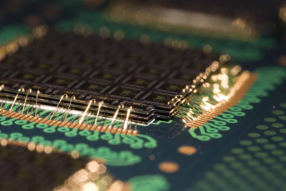

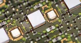

91
 BRAZIL Av. Prof.")

92 Henkel Your partner worldwide AMERICAS Henkel Corporation Barranca Parkway Irvine, CA HEADQUARTERS: UNITED STATES Barranca Parkway Irvine, CA Tel: Tel: CANADA 2225 Meadowpine Blvd. Mississauga, Ontario L5N 7P2 Tel: Tel: (within Canada) BRAZIL Av. Prof. Vernon Krieble, Itapevi, Sao Paulo, Brazil Tel: MEXICO Henkel Mexicana Boulevard Magnocentro No. 8 Centro Urbano Interlomas, Huixquilucan, Edo. de Mexico Tel: ASIA HEADQUARTERS: ASIA 928 Zhangheng Road, Zhangjiang Hi-Tech Park, Pudong New District, Shanghai, , P. R. China Tel: AUSTRALIA Unit South Street, Rydalmere 2216, Sydney, Australia Tel: CHINA 928 Zhangheng Road, Zhangjiang Hi-Tech Park, Pudong New District, Shanghai, , P. R. China Tel: INDIA No.1, Airport Service Road, Domlur Layout, Bangalore , India Tel: INDONESIA Jalan Raya Jakarta Bogor KM31.2, Cimanggis Depok 16953, Indonesia Tel: JAPAN 27-7 Shin Isogo-cho, Isogo-ku, Yokohama, Japan Tel: KOREA 1st Floor, Mapo-tower, 418, Mapo-dong, Mapo-gu, Seoul, Korea Tel: MALAYSIA Lot 973, Jalan Kampung Baru Hicom, Persiaran Tengku Ampuan, Lion Industrial Park, Sek 26, Shah Alam, Selangor, Malaysia Tel: PHILIPPINES 21/F, Asia Star Building, Asean Drive, Filinvest Corporate City, Alabang, Muntinlupa City 1781, Philippines Tel: SINGAPORE 401, Commonwealth Drive #03-01/02, Haw Par Techno Centre, Singapore Tel: TAIWAN 10/F, No.866, ZhongZheng Road, ZhongHe City, Taipei County 235, Taiwan Tel: Henkel Accurus , Wen-sien Road, Section 1 Jen-der, Tainan County Taiwan 717 Tel: THAILAND Centralworld, 35th Floor, 999/9 Rama 1 Road, Patumwan, Bangkok, 10330, Thailand Tel: EUROPE AUSTRIA See Henkel Germany BELGIUM Henkel Belgium N.V. Havenlaan 16 B-1080 Brussel Tel: +32-(0) BULGARIA Henkel Bulgaria E.O.O.D. Business Park Sofia Block 2, 4th floor BG-1715 Sofia Tel: CZECH REPUBLIC Henkel CR, spol. s r.o. U Pruhonu 10 CZ Praha 7 Tel: CROATIA Henkel Croatia d.o.o. Budmanijeva 1 HR Zagreb Tel DENMARK Henkel Norden AB, Copenhagen Horskaetten 3 DK-2630 Taastrup Tel: FINLAND Henkel Norden Oy Ayritie 12 a Vantaa Tel: FRANCE Henkel Loctite France 10, Avenue Eugene Gazeau BP F Senlis-Cedex Tel: GERMANY Henkel KGaA Gutenbergstrasse Garching Tel: +49 (0) HUNGARY Henkel Magyarorszag Kft. H-1113 Budapest David Ferenc u. 6 Tel: ITALY Henkel Loctite Adesivi S.r.l. Via Talete Brugherio (MI) Tel: NETHERLANDS Henkel Nederland B.V. Henkel Technologies Postbus CM Nieuwegein Tel: NORWAY Postboks: 6405 Etterstad 0604 Oslo Tel: POLAND Henkel Polska S.A. Domaniewska 41 PL Warszawa Tel: ROMANIA See Henkel Hungary RUSSIA RUSHENK Bakhrushina Ul., 32, Building 1 RU Moscow Tel: SLOVAKIA Henkel Slovensko s.r.o. Zahradnicka 91 P.O. Box 66 SK BRATISLAVA Tel: , 111 SPAIN Henkel Iberica, S.A. Pol. Ind. Alparrache Camino de Villaviciosa, 18 y Navalcarnero, Madrid Tel: SWEDEN Henkel Norden AB P.O. Box , SE Stockholm, Sweden Tel: SWITZERLAND See Henkel Germany TURKEY Türk Henkel Kimya Sanayi ve Ticaret A.S. Kayisdagi CadKaraman Ciftligi YoluKar Plaza D Blok Icerenköy - Istanbul, Turkey Tel: Fax: UKRAINE POW Henkel Ukraine Silver Centre 4, Lepse Blvd. UA Kiev Tel: IRELAND AND UK Henkel Loctite Adhesives Limited Technologies House Wood Lane End, Hemel Hempstead Hertfordshire HP2 4RQ Technologies House Tel: +44 (0) Across the Board, Around the Globe. and designate trademarks of Henkel Corporation or its Affiliates. = registered in the U.S. Patent and Trademark Office. Henkel Corporation, All rights reserved. 4531/LT-4842 (1/2008)
Die Attach Materials. Die Attach G, TECH. 2U. TECHNICAL R&D DIV.
 Die Attach Materials Die Attach G, TECH. 2U. TECHNICAL R&D DIV. 2 Topics 3 What it is X 5,000 X 10,000 X 50,000 Si Chip Au Plating Substrate Ag Resin 4 Current Products Characteristics H9890-6A H9890-6S
WS-575-C-RT. Halogen-Free Ball-Attach Flux PRODUCT DATA SHEET
 -RT Halogen-Free Ball-Attach Introduction Indium Corporation s Ball-Attach -RT allows customers to use a completely halogen-free (NIA = no intentionally added halogens) single-step ball-attach process
Henkel Enabling Materials for Semiconductor and Sensor Assembly. TechLOUNGE, 14 November 2017
 Henkel Enabling Materials for Semiconductor and Sensor Assembly TechLOUNGE, 14 November 2017 Content Brief HENKEL Introduction and ELECTRONICS Focus Areas Innovative Semiconductor and Sensor Assembly Solutions
Microelectronic Materials. Catalog
 Microelectronic Materials Catalog LORD partners with customers to leverage expertise in multiple chemistries and diverse applications to develop customized solutions. Design Without Compromise At LORD,
Microelectronic Materials CATALOG
 Microelectronic Materials CATALOG LORD partners with customers to leverage expertise in multiple chemistries and diverse applications to develop customized solutions. Design Without Compromise At LORD,
Basic PCB Level Assembly Process Methodology for 3D Package-on-Package
 Basic PCB Level Assembly Process Methodology for 3D Package-on-Package Vern Solberg STC-Madison Madison, Wisconsin USA Abstract The motivation for developing higher density IC packaging continues to be
Henkel Adhesive Solutions for SiP Packaging. October 17-19, 2018 Shanghai, China
 Henkel Adhesive Solutions for SiP Packaging October 17-19, 2018 Shanghai, China Agenda 1 2 3 4 Overview: Henkel Adhesive Electronics Semiconductor Market Trends & SiP Drivers Henkel Adhesive Solutions
The Development of a Novel Stacked Package: Package in Package
 The Development of a Novel Stacked Package: Package in Package Abstract Stacked die Chip Scale Packages (CSPs) or Fine-pitch BGAs (FBGAs) have been readily adopted and integrated in many handheld products,
WF6317. A superactive low-volatile/high heat-resistant water-soluble flux for ball soldering
 WF637 A superactive low-volatile/high heat-resistant water-soluble flux for ball soldering Low viscosity and high tacking power stabilize ball holding force and ensures excellent solder wettability Easy
Selection and Application of Board Level Underfill Materials
 Selection and Application of Board Level Underfill Materials Developed by the Underfill Materials Design, Selection and Process Task Group (5-24f) of the Assembly and Joining Committee (5-20) of IPC Supersedes:
Advancements In Packaging Technology Driven By Global Market Return. M. G. Todd
 Advancements In Packaging Technology Driven By Global Market Return M. G. Todd Electronic Materials, Henkel Corporation, Irvine, California 92618, USA Recently, the focus of attention in the IC packaging
Freescale Semiconductor Tape Ball Grid Array (TBGA) Overview
 Overview") Freescale Semiconductor Tape Ball Grid Array (TBGA) Overview Revision 0 2006 Freescale and the Freescale logo are trademarks of Freescale Semiconductor, Inc. All other product or service names are the
Freescale Semiconductor Tape Ball Grid Array (TBGA) Overview Revision 0 2006 Freescale and the Freescale logo are trademarks of Freescale Semiconductor, Inc. All other product or service names are the
Ultralow Residue Semiconductor Grade Fluxes for Copper Pillar Flip-Chip
 Ultralow Residue Semiconductor Grade Fluxes for Copper Pillar Flip-Chip SzePei Lim (Presenter), Jason Chou, Maria Durham, and Dr. Andy Mackie Indium Corporation 1 Outline of Presentation Roadmaps and challenges
EPOXY FLUX MATERIAL AND PROCESS FOR ENHANCING ELECTRICAL INTERCONNECTIONS
 As originally published in the SMTA Proceedings. EPOXY FLUX MATERIAL AND PROCESS FOR ENHANCING ELECTRICAL INTERCONNECTIONS Neil Poole, Ph.D., Elvira Vasquez, and Brian J. Toleno, Ph.D. Henkel Electronic
Asia/Pacific Semiconductor Packaging and Assembly Facilities, 2002 (Executive Summary) Executive Summary
 Executive Summary") Asia/Pacific Semiconductor Packaging and Assembly Facilities, 2002 (Executive Summary) Executive Summary Publication Date: October 24, 2002 Author Philip Koh This document has been published to the following
Asia/Pacific Semiconductor Packaging and Assembly Facilities, 2002 (Executive Summary) Executive Summary Publication Date: October 24, 2002 Author Philip Koh This document has been published to the following
!"#$"%&'()#*+,+-&.) )/01)"+.)101) )234)5"#$"%6+%)"7)"889) )!"#$"%6+%):&;-6:&<&+7') )=45&')*>)'6+%8&)#365)5"#$"%&')
#*+,+-&.) )/01)+.)101) )234)5#$%6+%)7)889) )!#$%6+%):&;-6:&<&+7') )=45&')*>)'6+%8&)#365)5#$%&')") !"#$"%&'()#*+,+-&.) )/01)"+.)101) )234)5"#$"%6+%)"7)"889) )!"#$"%6+%):&;-6:&)'6+%8&)#365)5"#$"%&') plastic ceramic DIP DIL PDIP CDIP CerDIP MDIP FDIP SDIP JLCC PLCC CLCC QFP PQFP HQFP RQFP
!"#$"%&'()#*+,+-&.) )/01)"+.)101) )234)5"#$"%6+%)"7)"889) )!"#$"%6+%):&;-6:&)'6+%8&)#365)5"#$"%&') plastic ceramic DIP DIL PDIP CDIP CerDIP MDIP FDIP SDIP JLCC PLCC CLCC QFP PQFP HQFP RQFP
Challenges in Material Applications for SiP
 Challenges in Material Applications for SiP Sze PeiLim Regional Product Manager for Semiconductor Products Indium Corporation Indium Corporation Materials Supplier: SMT solder pastes and fluxes Power semiconductor
Encapsulation Selection, Characterization and Reliability for Fine Pitch BGA (fpbga )
") Encapsulation Selection, Characterization and Reliability for Fine Pitch BGA (fpbga ) Henry M.W. Sze, Marc Papageorge ASAT Limited 14th Floor, QPL Industrial Building, 138 Texaco Road, Tseun Wan, Hong
Encapsulation Selection, Characterization and Reliability for Fine Pitch BGA (fpbga ) Henry M.W. Sze, Marc Papageorge ASAT Limited 14th Floor, QPL Industrial Building, 138 Texaco Road, Tseun Wan, Hong
Novel Materials and Activities for Next Generation Package. Hitachi Chemical., Co.Ltd. Packaging Solution Center Hiroaki Miyajima
 Novel Materials and Activities for Next Generation Package Hitachi Chemical., Co.Ltd. Packaging Solution Center Hiroaki Miyajima 1. Activities of Packaging Solution Center 2. Novel Materials for Next Gen.
Selector Guide. Providing the Connections for your Success. Automotive ele c tronics
 Providing the Connections for your Success Selector Guide Automotive ele c tronics Conductive Adhesives - Materials for Harsh Environment Protection - Underfill Encapsulants Electrically Conductive Adhesives
MEMS. Micro-Electro-Mechanical Systems
 Redline : Opt + 2 Henkel Electronics MEMS Micro-Electro-Mechanical Systems MEMS Henkel Electronic Advantage When one considers the average smartphone contains approximately eight to 10 MEMS a number which
Recent Advances in Die Attach Film
 Recent Advances in Die Attach Film Frederick Lo, Maurice Leblon, Richard Amigh, and Kevin Chung. AI Technology, Inc. 70 Washington Road, Princeton Junction, NJ 08550 www.aitechnology.com Abstract: The
BGA Package Underfilm for Autoplacement. Jan Danvir Tom Klosowiak
 BGA Package Underfilm for Autoplacement Jan Danvir Tom Klosowiak NIST-ATP Acknowledgment Project Brief Microelectronics Manufacturing Infrastructure (October 1998) Wafer-Scale Applied Reworkable Fluxing
S/C Packaging Assembly Challenges Using Organic Substrate Technology
 S/C Packaging Assembly Challenges Using Organic Substrate Technology Presented by Bernd Appelt ASE Group Nov. 17, 2009 Overview The Packaging Challenge Chip Substrate Interactions Stiffeners for FC-BGA
United Adhesives. Aerospace Automotives Computers Electronics Green Energy Semiconductors Telecommunications
 United Adhesives Aerospace Automotives Computers Electronics Green Energy Semiconductors Telecommunications Welcome to United Adhesives, Inc. United Adhesives Inc. formulates and manufactures special adhesives
CONTENTS INTRODUCTION. Underfills... 11
 FINGERPRINT SENSORS CONTENTS Introduction... 2 Product Portfolio... 5 Adhesives in Action... 6 Glass to IC Attach... 8 Electrically Conductive Adhesives... 9 Sensor Die Attach Materials...10 Underfills...
Green IC packaging: A threath to electronics reliability
 Green IC packaging: A threath to electronics reliability Geert Willems Steven Thijs, Bart Vandevelde imec 13 juni 2012 Bits & Chips Hardware Conference Content 1. Plastic Molding Compounds 2. Towards Green,
Flip Chip - Integrated In A Standard SMT Process
 Flip Chip - Integrated In A Standard SMT Process By Wilhelm Prinz von Hessen, Universal Instruments Corporation, Binghamton, NY This paper reviews the implementation of a flip chip product in a typical
MEPTEC Semiconductor Packaging Technology Symposium
 MEPTEC Semiconductor Packaging Technology Symposium Advanced Packaging s Interconnect Technology Process Shift and Direction October 23, 2014 Jay Hayes- Director of Business Development -Bumping and Flip
Assembly Reliability of TSOP/DFN PoP Stack Package
 As originally published in the IPC APEX EXPO Proceedings. Assembly Reliability of TSOP/DFN PoP Stack Package Reza Ghaffarian, Ph.D. Jet Propulsion Laboratory, California Institute of Technology Pasadena,
ELEC 6740 Electronics Manufacturing Chapter 5: Surface Mount Design Considerations
 ELEC 6740 Electronics Manufacturing Chapter 5: Surface Mount Design Considerations R. Wayne Johnson Alumni Professor 334-844 844-1880 johnson@eng.auburn. @eng.auburn.eduedu Outline System Design Issues
ELEC 6740 Electronics Manufacturing Chapter 5: Surface Mount Design Considerations
 ELEC 6740 Electronics Manufacturing Chapter 5: Surface Mount Design Considerations R. Wayne Johnson Alumni Professor 334-844-1880 johnson@eng.auburn. @eng.auburn.eduedu Outline System Design Issues Package
23 rd ASEMEP National Technical Symposium
 THE EFFECT OF GLUE BOND LINE THICKNESS (BLT) AND FILLET HEIGHT ON INTERFACE DELAMINATION Raymund Y. Agustin Janet M. Jucar Jefferson S. Talledo Corporate Packaging & Automation/ Q&R STMicroelectronics,
ALPHA OM-5100 FINE PITCH SOLDER PASTE
 SM 797-7 ALPHA OM-5100 FINE PITCH SOLDER PASTE DESCRIPTION Cookson Electronics Assembly Material s ALPHA OM-5100, is a low residue, no-clean solder paste designed to maximize SMT line yields. The flux
Environmental Management and Materials Information
 Environmental Management and Materials Information Product Content Information for: MAX3674ECM+T Links Qualifications Package Description Chemical Composition Detailed Package Component Data Qualifications
3D-WLCSP Package Technology: Processing and Reliability Characterization
 3D-WLCSP Package Technology: Processing and Reliability Characterization, Paul N. Houston, Brian Lewis, Fei Xie, Ph.D., Zhaozhi Li, Ph.D.* ENGENT Inc. * Auburn University ENGENT, Inc. 2012 1 Outline Packaging
5. Packaging Technologies Trends
 5. Packaging Technologies Trends Electronic products and microsystems continue to find new applications in personal, healthcare, home, automotive, environmental and security systems. Advancements in packaging
LS720V Series. Comparison of crack progression between Sn-Cu-Ni-Ge and M773. Development of Ag-free/M773 alloy
 LS72V Series Low-Ag/Ag-free solder pastes with lower void Reduces voids by improving fluidity of flux during solder melting Reduces voids even in bottom surface electrode type components by improving solder
Organic Flip Chip Packages for Use in Military and Aerospace Applications. David Alcoe, Kim Blackwell and Irving Memis, Endicott NY
 Organic Flip Chip Packages for Use in Military and Aerospace Applications David Alcoe, Kim Blackwell and Irving Memis, Endicott NY 1 Contents 1. Bridge from Commercial Reliability 2. Existing PBGA use
Environmental Management and Materials Information
 Environmental Management and Materials Information Product Content Information for: MAX44285FAWA+ Links Qualifications Package Description Chemical Composition Detailed Package Component Data Other Component
Advanced Analytical Techniques for Semiconductor Assembly Materials and Processes. Jason Chou and Sze Pei Lim Indium Corporation
 Advanced Analytical Techniques for Semiconductor Assembly Materials and Processes Jason Chou and Sze Pei Lim Indium Corporation Agenda Company introduction Semiconductor assembly roadmap challenges Fine
Hi-performance S3X58-M406
 www.ko-ki.co.jp Ver. 42004.5 Prepared on Mar. 7, 2005 Koki no-clean LEAD FREE solder paste Hi-performance Product information 0.4mm pitch 0.3mm diameter This Product Information contains product performance
Wire-Bond CABGA A New Near Die Size Packaging Innovation Yeonho Choi February 1, 2017
 Amkor Technology, Inc. White Paper Wire-Bond CABGA A New Near Die Size Packaging Innovation Yeonho Choi February 1, 2017 Abstract Expanding its ChipArray Ball Grid Array (CABGA) package form factor miniaturization
Failure Modes in Wire bonded and Flip Chip Packages
 Failure Modes in Wire bonded and Flip Chip Packages Mumtaz Y. Bora Peregrine Semiconductor San Diego, Ca. 92121 mbora@psemi.com Abstract The growth of portable and wireless products is driving the miniaturization
SLIM TM, High Density Wafer Level Fan-out Package Development with Submicron RDL
 2017 IEEE 67th Electronic Components and Technology Conference SLIM TM, High Density Wafer Level Fan-out Package Development with Submicron RDL YoungRae Kim 1, JaeHun Bae 1, MinHwa Chang 1, AhRa Jo 1,
The Packaging and Reliability Qualification of MEMS Resonator Devices
 The Packaging and Reliability Qualification of MEMS Resonator Devices Pavan Gupta Vice President, Operations Yin-Chen Lu, Preston Galle Quartz and MEMS Oscillators source: www.ecliptek.com Quartz Oscillators:
McKinney, Texas. McKinney, Texas, Cheshire, CT, Morrisville, NC USA
 McKinney, Texas McKinney, Texas, Cheshire, CT, Morrisville, NC USA http://www.m-coat.com Just like an old friend, we can do it all Military Microelectronics Electronics Medical Conductive silvers Encapsulants
HIGH QUALITY THERMALLY CONDUCTIVE MATERIALS
 14.february.2011 HIGH QUALITY THERMALLY CONDUCTIVE MATERIALS Table of contents Non-silicone compounds (Tim4xx series)... section 1 Silicone compounds (Tim5xx series)... section 1 Dielectric silicone grease
Koki no-clean LEAD FREE solder paste. High-reliability Low Ag Lead Free Solder Paste
 www.ko-ki.co.jp #514- Revised on Feb.4, 214 Koki no-clean LEAD FREE solder paste High-reliability Low Ag Lead Free Solder Paste S1XBIG58-M5-4 Product information S1XBIG SAC35 After -4/125ºC, 1 cycles This
S3X48-M500C-5. Powerful Wetting Lead Free Solder Paste. Product information. Koki no-clean LEAD FREE solder paste. Contents.
 Koki no-clean LEAD FREE solder paste www.ko-ki.co.jp #50011E-0 Revised on JAN.22, 2013 Powerful Wetting Lead Free Solder Paste Product information This Product Information contains product performance
Semiconductor IC Packaging Technology Challenges: The Next Five Years
 SPAY025 May 2006 White Paper Mario A. Bolanos, Director Semiconductor Group Packaging Technology Development, Texas Instruments In the era of communications and entertainment, growth of consumer electronics
POTTING & ENCAPSULATING
 POTTING & ENCAPSULATING ASSEMBLY PRODUCTS 38 POTTING & ENCAPSULATING Potting and Encapsulating Compounds are used to provide mechanical reinforcement to housed assemblies, to fill large voids, and to protect
Design and Characterization of Thermal Conductive Wafer Coating in Thin Small Outline Package for Automotive Product Application
 Design and Characterization of Thermal Conductive Wafer Coating in Thin Small Outline Package for Automotive Product Application Azhar Abdul Hamid, Dhanapalan Periathamby, *Suhaimi Azizan, Chee Eng Tan,
Fundamentals of Sealing and Encapsulation
 Fundamentals of Sealing and Encapsulation Sealing and Encapsulation Encapsulation and sealing are two of the major protecting functions of IC packaging. They are used to protect IC devices from adverse
Typical Analysis Sn Ag Cu Pb Sb Bi In As Fe Ni Cd Al Zn Au
 TECHNICAL SPECIFICATIONS Physical Properties Solder Composition Qualitek Sn/Ag/Cu (Tin/Silver/Cu) Alloys are designed as a lead-free alternative for Sn/Pb alloys for electronics assembly operations. The
White Paper Quality and Reliability Challenges for Package on Package. By Craig Hillman and Randy Kong
 White Paper Quality and Reliability Challenges for Package on Package By Craig Hillman and Randy Kong Background Semiconductor technology advances have been fulfilling Moore s law for many decades. However,
Trends and Developments
 Trends and Developments Monique Mayr Monique.Mayr@eu.panasonic.com European R&M Group Panasonic Corporation Electronic Material Business Division Weitere Informationen finden Sie auch auf: http://www3.panasonic.biz/em/pcbm/en/index.html
CX Thin Fil s. Resistors Attenuators Thin-Film Products Thin-Film Services. ISO 9001:2008 RoHS/REACH Compliant ITAR Compliant
 CX Thin Fil s Resistors Attenuators Thin-Film Products Thin-Film Services www.cxthinfilms.com ISO 9001:2008 RoHS/REACH Compliant ITAR Compliant www.cxthinfilms.com sales@cxthinfilms.com +1 (401) 461-5500
Material based challenge and study of 2.1, 2.5 and 3D integration
 1 Material based challenge and study of 2.1, 2.5 and 3D integration Toshihisa Nonaka Packaging Solution Center R&D Headquarters Hitachi Chemical Co., Ltd., Sep. 8, 2016 Hitachi Chemical Co., Ltd. 2010.
Design and Assembly Process Implementation of 3D Components
 IPC-7091 Design and Assembly Process Implementation of 3D Components Developed by the 3-D Electronic Packages Subcommittee (B-11) of the Packaged Electronic Components Committee (B-10) of IPC Users of
Assembly and Rework of Lead Free Package on Package Technology By: Raymond G. Clark and Joseph D. Poole TT Electronics - IMS Perry, Ohio
 Assembly and Rework of Lead Free Package on Package Technology By: Raymond G. Clark and Joseph D. Poole TT Electronics - IMS Perry, Ohio Abstract: Miniaturization continues to be a driving force in both
T E C H N I C A L B U L L E T I N
 T E C H N I C A L B U L L E T I N SM1193 ALPHA CVP-390 SAC305- HIGH PERFORMANCE LEAD-FREE ALLOY SOLDER PASTE FOR AUTOMOTIVE ELECTRONICS DESCRIPTION CVP-390 SAC305 solder paste has been developed to provide
IPC-AJ-820A Assembly and Joining Handbook. The How and Why of All Things PCB & PCA
 IPC-AJ-820A Assembly and Joining Handbook The How and Why of All Things PCB & PCA 1 Scope To provide guidelines and supporting info for the mfg of electronic equipment To explain the HOW TO and WHY Discussions
PASSIVE COMPONENT MATERIALS HIMEC, UNIMEC, OHMCOAT
 PASSIVE COMPONENT MATERIALS HIMEC, UNIMEC, OHMCOAT PRODUCT RANGE Sintering Materials =>> HIMEC Used for Electrodes on Passive Components For Photovoltaic Pastes (Front Side & Back Side Silver Paste ) For
Features Conductive Room Temperature Cure. Product Ref IP 4525IP Low viscosity adhesive & coating. High thermal conductivity
 Properties and Part Selection Overview Selection Table - Epoxy-Based Adhesive Properties Features Conductive Room Temperature Cure Product Ref 120 132 4461IP 42IP 438 700 Properties High electrical conductivity
LED Die Attach Selection Considerations
 LED Die Attach Selection Considerations Gyan Dutt & Ravi Bhatkal Alpha, An Alent plc Company Abstract Die attach material plays a key role in performance and reliability of mid, high and super-high power
Lead Free Solder for Flip Chip
 Lead Free Solder for Flip Chip Zhenwei Hou & R. Wayne Johnson Laboratory for Electronics Assembly & Packaging Auburn University 162 Broun Hall, ECE Dept. Auburn, AL 36489 USA 334-844-1880 johnson@eng.auburn.edu
Lighting the way in LED Applications
 Lighting the way in LED Applications The global market for packaged LED is expected to reach US$18.54 billion by 2021 Source: Yole Développement The future of lighting Rapid growth of the LED market In
Outline. Market Size Industry Trends Material Segment Trends China Summary. Packaging Materials Market Trends, Issues and Opportunities
 Packaging Materials Market Trends, Issues and Opportunities Dan Tracy Sr. Director Industry Research SEMI 8 th December 2015 Outline Market Size Industry Trends Material Segment Trends China Summary 1
3D Package Technologies Review with Gap Analysis for Mobile Application Requirements. Apr 22, 2014 STATS ChipPAC Japan
 3D Package Technologies Review with Gap Analysis for Mobile Application Requirements Apr 22, 2014 STATS ChipPAC Japan T.Nishio Contents Package trends and roadmap update Advanced technology update Fine
Material Selection and Parameter Optimization for Reliable TMV Pop Assembly
 Selection and Parameter Optimization for Reliable TMV Pop Assembly Brian Roggeman, David Vicari Universal Instruments Corp. Binghamton, NY, USA Roggeman@uic.com Martin Anselm, Ph.D. - S09_02.doc Lee Smith,
Gap Filler Liquid Dispensed Materials
 26 Thermal Interface Selection Guide Gap Filler Liquid Dispensed Materials Introduction Effective thermal management is key to ensuring consistent performance and long-term reliability of many electronic
EVALUATION OF HIGH RELIABILITY REWORKABLE EDGE BOND ADHESIVES FOR BGA APPLICATIONS
 As originally published in the SMTA Proceedings. EVALUATION OF HIGH RELIABILITY REWORKABLE EDGE BOND ADHESIVES FOR BGA APPLICATIONS Fei Xie, Ph.D., Han Wu, Daniel F. Baldwin, Ph.D., Swapan Bhattacharya,
Effect of Die Bonding Condition for Die Attach Film Performance in 3D QFN Stacked Die.
 Effect of Die Bonding Condition for Die Attach Film Performance in 3D QFN Stacked Die. A. JALAR, M. F. ROSLE, M. A. A. HAMID. School of Applied Physics, Faculty of Science and Technology Universiti Kebangsaan
DSP 863 (Sn42/Bi58) LEAD FREE HALOGEN FREE NO CLEAN SOLDER PASTE
 LEAD FREE HALOGEN FREE NO CLEAN SOLDER PASTE") SN/AG/CU. 862 Rev.A TECHNICAL DATA SHEET TECHNICAL SPECIFICATIONS SN/AG/CU. 862 Rev DSP 863 (Sn42/Bi58) LEAD FREE HALOGEN FREE NO CLEAN SOLDER PASTE CORPORATE HEADQUARTERS USA: 315 Fairbank St. Addison,
SN/AG/CU. 862 Rev.A TECHNICAL DATA SHEET TECHNICAL SPECIFICATIONS SN/AG/CU. 862 Rev DSP 863 (Sn42/Bi58) LEAD FREE HALOGEN FREE NO CLEAN SOLDER PASTE CORPORATE HEADQUARTERS USA: 315 Fairbank St. Addison,
Adaption to scientific and technical progress under Directive 2002/95/EC
 . Adaption to scientific and technical progress under Directive 2002/95/EC Results previous evaluation Exemption No. 15 Lead in solders to complete a viable electrical connection between semiconductor
Challenges and Solutions for Cost Effective Next Generation Advanced Packaging. H.P. Wirtz, Ph.D. MiNaPAD Conference, Grenoble April 2012
 Challenges and Solutions for Cost Effective Next Generation Advanced Packaging H.P. Wirtz, Ph.D. MiNaPAD Conference, Grenoble April 2012 Outline Next Generation Package Requirements ewlb (Fan-Out Wafer
Novel Technique for Flip Chip Packaging of High power Si, SiC and GaN Devices. Nahum Rapoport, Remtec, Inc.
 Novel Technique for Flip Chip Packaging of High power Si, SiC and GaN Devices Nahum Rapoport, Remtec, Inc. 1 Background Electronic Products Designers: under pressure to decrease cost and size Semiconductor
Epoxy. Epoxy 90, ,000. Epoxy. Epoxy. low ion content, Encapsulation of electronic
 - - and Light Curing Adhesives Our comprehensive range of systems covers a multitude of applications and offers many advantages: systems are used in many fields in both trade and industry. adhesives and
Manufacturing and Reliability Challenges With QFN
 Manufacturing and Reliability Challenges With QFN Dr. Craig Hillman and Cheryl Tulkoff DfR Solutions SMTA DC Chapter Ashburn, VA February 25, 2009 QFN as a Next Generation Technology What is Next Generation
Adaption to scientific and technical progress under Directive 2002/95/EC
 . Adaption to scientific and technical progress under Directive 2002/95/EC Results previous evaluation Exemption No. 7 a a) Lead in high melting temperature type solders (i.e. lead-based alloys containing
IME Technical Proposal. High Density FOWLP for Mobile Applications. 22 April High Density FOWLP Consortium Forum
 IME Technical Proposal High Density FOWLP for Mobile Applications 22 April 2014 Packaging driver for portable / mobile applications Key drivers/needs Smaller form-factor lower profile, substrate-less Higher
High-Reliability Lead-Free Solder Paste M705-GRN360-K-V. Senju Metal Industry Co.,Ltd. Senju Manufacturing (Europe) Ltd.
 Ltd.") Senju Metal Industry Co., Ltd. High-Reliability Lead-Free Solder Paste Manufacturer Senju Metal Industry Co.,Ltd. 23 Senju Hashido-cho, Adachi-Ku, Tokyo, Japan Phone: +81-33888-5156 Fax: +81-33870-3032
Senju Metal Industry Co., Ltd. High-Reliability Lead-Free Solder Paste Manufacturer Senju Metal Industry Co.,Ltd. 23 Senju Hashido-cho, Adachi-Ku, Tokyo, Japan Phone: +81-33888-5156 Fax: +81-33870-3032
Chips Face-up Panelization Approach For Fan-out Packaging
 Chips Face-up Panelization Approach For Fan-out Packaging Oct. 15, 2015 B. Rogers, D. Sanchez, C. Bishop, C. Sandstrom, C. Scanlan, TOlson T. REV A Background on FOWLP Fan-Out Wafer Level Packaging o Chips
Environmental Management and Materials Information
 Environmental Management and Materials Information Product Content Information for: MAX3622CUE+ Links Qualifications Package Description Chemical Composition Detailed Package Component Data Qualifications
Low Melting Point Lead Free Solder Paste
 www.ko-ki.co.jp #49005E Revised on Nov 17, 2011 Koki no-clean LEAD FREE solder paste Koki no-clean LEAD FREE solder paste Low Melting Point Lead Free Solder Paste TB48-M742 & Product information This Product
Avatrel Stress Buffer Coatings: Low Stress Passivation and Redistribution Applications
 Avatrel Stress Buffer Coatings: Low Stress Passivation and Redistribution Applications Ed Elce, Chris Apanius, Jeff Krotine, Jim Sperk, Andrew Bell, Rob Shick* Sue Bidstrup-Allen, Paul Kohl Takashi Hirano,
Potting & Encapsulating
 Potting & Encapsulating Potting and encapsulating compounds are used to provide mechanical reinforcement to housed assemblies, to fill large voids, and to protect components from the effects of exposure
UMC UM F-7 2M-Bit SRAM
 Construction Analysis UMC UM 613264F-7 2M-Bit SRAM Report Number: SCA 9609-511 Global Semiconductor Industry the Serving Since 1964 15022 N. 75th Street Scottsdale, AZ 85260-2476 Phone: 602-998-9780 Fax:
Gap Filler 1000 (Two-Part)
") Gap Filler 1000 (Two-Part) Thermally Conductive, Liquid Gap Filling Material Thermal conductivity: 1.0 W/m-K Ultra-conforming, designed for fragile and low-stress applications Ambient and accelerated cure
Gap Filler 1000 (Two-Part) Thermally Conductive, Liquid Gap Filling Material Thermal conductivity: 1.0 W/m-K Ultra-conforming, designed for fragile and low-stress applications Ambient and accelerated cure
ALTERNATIVES TO SOLDER IN INTERCONNECT, PACKAGING, AND ASSEMBLY
 ALTERNATIVES TO SOLDER IN INTERCONNECT, PACKAGING, AND ASSEMBLY Herbert J. Neuhaus, Ph.D., and Charles E. Bauer, Ph.D. TechLead Corporation Portland, OR, USA herb.neuhaus@techleadcorp.com ABSTRACT Solder
Edge Bond Package joint reinforcement JU-120EB Product Information
 www.ko-ki.co.jp #55023 First issue on October 25, 2017 Revised on Koki Adhesive Edge Bond Package joint reinforcement Product Information BGA body Disclaimer This Product Information contains product performance
CHALLENGING NEW TECHNOLOGIES
 T4AB58-M742 Koki no-clean LEAD FREE solder paste www.ko-ki.co.jp #49005-1 Revised on Sep. 30, 2014 Koki no-clean LEAD FREE solder paste Low Melting Point Lead Free Solder Paste T4AB58-M742 Product information
Illuminating Innovations
 Illuminating Innovations TM Silicone Solutions for LED Packaging Emir Debastiani Application Engineer Dow Corning Brazil Email: emir.debastiani@dowcorning.com Table of Contents Dow Corning Introduction
IPC -7095C Design and Assembly Process Implementation For BGAs
 IPC -7095C Design and Assembly Process Implementation For BGAs 1 Overview With the introduction of BGA components, things had to change: New design New assembly process New repair process New inspection
TIN-BASED LEAD-FREE SOLDER BUMPS FOR FLIP-CHIP APPLICATION. S. Yaakup, H. S. Zakaria, M. A. Hashim and A. Isnin
 TIN-BASED LEAD-FREE SOLDER BUMPS FOR FLIP-CHIP APPLICATION S. Yaakup, H. S. Zakaria, M. A. Hashim and A. Isnin Advanced Materials Research Centre (AMREC), SIRIM Berhad, Lot 34, Jalan Hi-Tech 2/3, Kulim
TECHNICAL INFORMATION. Dispensing LEAD FREE No-clean SOLDER PASTE S3X58 - M406D. [ Contents ]
![TECHNICAL INFORMATION. Dispensing LEAD FREE No-clean SOLDER PASTE S3X58 - M406D. [ Contents ]](/thumbs/88/115442512.jpg "TECHNICAL INFORMATION. Dispensing LEAD FREE No-clean SOLDER PASTE S3X58 - M406D. [ Contents ]") Lead free SOLUTIONS you can TRUST TECHNICAL INFORMATION Dispensing LEAD FREE No-clean SOLDER PASTE S3X58 - M406D [ Contents ] 1. FEATURES...Page 2 2. SPECIFICATIONS... 2 3. ALLOY PROPERTIES... 3 4. DISPENSABILITY...
Lead free SOLUTIONS you can TRUST TECHNICAL INFORMATION Dispensing LEAD FREE No-clean SOLDER PASTE S3X58 - M406D [ Contents ] 1. FEATURES...Page 2 2. SPECIFICATIONS... 2 3. ALLOY PROPERTIES... 3 4. DISPENSABILITY...
Materials for Wearable Electronics. At A Glance
 Materials for Wearable Electronics At A Glance INTRODUCTION From watches to fitness bands to textiles and jewelry, wearable electronics are what many believe could be the next big or small thing in electronics.
Nanium Overview. Company Presentation
 Nanium Overview Company Presentation Nanium Overview Our name and logo nano prefix of Greek origin referring to small objects ium suffix of Latin origin that includes the formation of scientific terms