Challenges and Solutions for Cost Effective Next Generation Advanced Packaging. H.P. Wirtz, Ph.D. MiNaPAD Conference, Grenoble April 2012
|
|
|
- Millicent Payne
- 6 years ago
- Views:
Transcription

1 Challenges and Solutions for Cost Effective Next Generation Advanced Packaging H.P. Wirtz, Ph.D. MiNaPAD Conference, Grenoble April 2012
2 Outline Next Generation Package Requirements ewlb (Fan-Out Wafer Level package) Introduction to ewlb Innovations in ewlb platform ewlb Status at STATS ChipPAC fccube Summary 2
3 Next Generation Package Requirements (Mobile) Shrink on silicon: 32nm, 28nm 20nm Wafer size increase will impact FE assy PCB Area Mobile product form factor SIP/MCP solutions for early modem integration to reduce number of packages Handle increasing IO count per silicon area Package thickness mobile product form factor POP thickness reduction to < 1.0 mm including 2 die memory BGA thickness 0.8mm System Integration Enable easy platform design at customer level SI/PI at package level e.g. embedded decoupling Package ball-out in line with customer PCB build-up targets Thermal Performance Peak performance limited by package design Non-POP side-by-side memory solutions for tablets Exposed die heat spreader for AP New materials for increased thermal conductivity lateral and towards top and PCB 3D Integration Manufacturing and test solutions Backside processing, assembly and test of Wide-IO application processors Cost - Cost - Cost Cost reduction strategies for existing technologies 3


4 What is ewlb? Wafer Level Packaging technology, utilizes well developed wafer bumping infrastructure, with an innovative wafer reconstitution process to package Known Good Dice. Wafer level package, uses mold compound to support the fan-out I/Os. Fan-In WLP PKG size = Chip size ewlb/fan-out WLP PKG size > Chip size chip Fan-In Interconnects only - Number and pitch of Interconnects must be adapted to the chip size Only Single chip packaging solution ewlb expands the application space for Wafer Level Packaging! Fan-out Interconnects - #, Pitch of Interconnect is INDEPENDENT of chip size Single/Multi/3D chip packaging solution Improved Yield with KGD 4


 ewlb (fan-out)")
5 ewlb Configuration comparison between fan-in vs. fan-out WLP - ewlb is the best fan-out wafer scale package Conventional WLP (fan-in) ewlb (fan-out) footprint larger than die 5
 The thinnest 3D solution (down to 0.")
 and maximum I/O density Excellent electrical and thermal performance High bandwidth wide I/O 3D incorporating TSV Enhanced reliability")
6 Form Factor, Performance & Integration Superior Solutions spanning the needs of mobile and other high-performance applications MCP configurations (down to 0.5mm) The thinnest 3D solution (down to 0.8mm) Scalable heterogeneous integration platform Leading cost/performance solutions (co-design optimized) Ultra fine ball pitch (down to 0.3mm) and maximum I/O density Excellent electrical and thermal performance High bandwidth wide I/O 3D incorporating TSV Enhanced reliability with advanced dielectric materials MLP-PoP configurations - both single and double sided 6


7 ewlb Products Portfolio 2D ewll 2.5D / Extended ewlb ewlb-mlp ewlb is a powerful wafer level and integration solutions platform 7


 250mm thin")

 ewlb")
8 Next Generation ewlb 10mm/10mm line width and line spacing Plated Cu RDL 10mm Thin packaging solution (<0.5mm) 250mm thin ewlb for more design and routing flexibility 3D (double-side) ewlb Multi-die ewlb Embedded Passives 8


9 New packages in ewlb platform Small outline ewlb 3D SiP ewlb (double-side RDL) 2.4x2.4mm ewlb with 2x2mm die, 0.4mm pitch 200um ewlb PoP (ewlb + ewlb/bga) ewll ewlb-pop (single-side RDL) 9
 Integration TSV Interposer based solution Logic Analog Thin TSV interposer (TSI) fabrication Logic & Analog bumping Integration of multiple dies to the thin TSI with underfill Integration of")
10 Heterogeneous (2.5D) Integration TSV Interposer based solution Logic Analog Thin TSV interposer (TSI) fabrication Logic & Analog bumping Integration of multiple dies to the thin TSI with underfill Integration of TSI-tosubstrate with underfill Package Assembly ewlb based Solution Extended ewlb Logic Analog ewlb fabrication Integration of ewlb to the substrate with underfill Package Assembly Organic substrate ewlb provides a 2.5D integration platform superior to conventional TSV Interposer (TSI) based solutions in overall cost and process simplicity 10
 + 3x4mm) I/O Count: 396 1-L RDL (Top and Bottom both) Thickness 450um /")
 Low profile 3D ewlb PoP (12x12mm PoP-bottom package) with less")
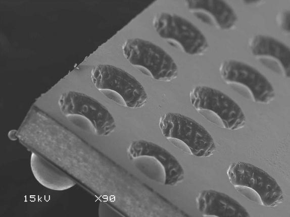
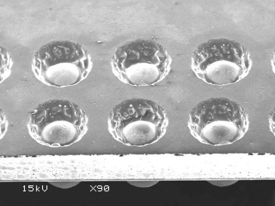
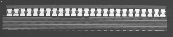
11 Double-side 3D SiP ewlb Test Vehicle Specification PKG: 12x12sqmm, 0.5mm ball pitch Die : 3-die, 2 (3x3mm) + 3x4mm) I/O Count: L RDL (Top and Bottom both) Thickness 450um / 250um 1.2mm 450um 250um 250um Thin Bottom 3D PKG <1.0mm Picture of 3D ewlb PoP packages; Total less than 1.0 mm package height (including solder balls) Low profile 3D ewlb PoP (12x12mm PoP-bottom package) with less than 1mm thickness including solder balls. 11
 Lower warpage during solder reflow cycles")
 Q JB 3~7( o C/W) for 12x12mm ewmlp) Memory + Si")
12 Ultra Low Profile ewlb PoP: ewlb-pop ewlb 3D Interconnects ewlb-pop Successfully qualified for CLR & BLR Thin POP (250um pkg body thickness) Lower warpage during solder reflow cycles Flexibility in memory interface High routing density: L/S=10/10 (um) Compatible with ELK Good thermal performance Q JA 18~22( o C/W) Q JB 3~7( o C/W) for 12x12mm ewmlp) Memory + Si RDL 12

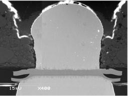
13 ewlb-pop Bottom Package Cross-Sections Si RDL 13
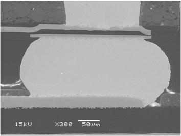
14 ewlb PoP Cross-Sections 14


 Unit")
 Stretch the")


15 ewlb Cost-reduction path Wafer size Available area increase (Area ratio ~ 2.35) Higher yield in 12 ( >99%) Unit cost decrease ( -25~30%) Stretch the limits 200mm size 8 HVM from mm HVM from New Technology (Panel, size under investigation) 15

16 FO-WLP (ewlb) / Embedded Die Substrate Fan-Out WLP (ewlb) Embedded Die Substrate No substrate Miniaturized and high performance Full module approach with free top surface In HVM 2009, Proven yield > 98% Batch/inline process of wafer level Replacing / Competing with embedding Embedding die in mold during assembly/packaging Simple logistics and supply chain Embedded Active or Chip-in-Substrate (CIS) Achieve PWB design miniaturization Need Cu plating on die Yield concerns of high density substrate Few modules seen in Japanese market since 2005 Embedding die in substrate by substrate manufacturer Complex logistics; how to involve substrate maker Supply chain Component testing Ownership 16

 Pad w/ Open SR")
 -> 20N")

 Cost savings / higher production throughput")

17 fccube - Value Proposition! High Performance l High I/O Density l ELK/ULK Reliability l Fab Node Compatibility Copper (Cu) Column with Pb-Free Cap High I/O density Very fine bump pitch to 80um Superior electro-migration resistance Green package Bond on Lead (BOL) Pad w/ Open SR Structure High I/O density Design rule relaxation Lower cost w/ layer count reduction And No SOP Elimination of ELK/ULK Damage on Advanced Si Nodes (40/28nm) -> 20N Scalability to Fine Bump Pitches down to 40um! Spanning a wide bump pitch spectrum using Cu-column FC TM Flip Chip Redefined Package Types fcbga, fcfbga (fccsp) fcpop / MLP(3D) TSV Mold Underfill (MUF) with Cu column bump Enhanced to fill fine gap (<50u) Cost savings / higher production throughput Potential package size reduction Optimization of Material Flow & Equipment Selection catered to Customer Design Higher production throughput Cost savings 2-Layer Laminate using no-sop, BOL, Open SRO Design 50% cost reduction vs std FC Relaxed substrate design rules Dense routing 17 17

 w/ MR & NCP w/ TCB Compatibility fccube Assembly Options Pkg.")

18 fccube Technology Supports Full Range of Product needs Across all Fab Nodes and Bump Pitches! fccube Technology offers optional Interconnection methods: Mass Reflow or Thermo Compression Bonding Allows maximum flexibility in meeting key design requirements across all fab nodes & fine Bump Pitches Core fccube Technology Interconnect Structure Underfill Copper (Cu) Column with Pb-Free Cap, with BOL Pad and Open SR Mold Underfill (MUF) w/ MR & NCP w/ TCB Compatibility fccube Assembly Options Pkg. Types (fcfbga/ MLP/ fcbga) Fab Nodes Assembly Process Primary Benefit Mass Reflow (fccube-mf) Mainstream (infrastructure friendly) & Low Cost 80 40N- >28N - > 20N - > 14N Thermo Compression Bonding (fccube-tcb) Suitable for ultra-high density e.g. TSV Si-to-Si f-t-f/f-t-b bonding fccube Interconnect Option using Mass Reflow (MR) or Thermo Compression Bonding (TCB) offers flexibility to optimize cost / pitch / performance based on Si Node, I/O design, product timing., etc. 18
19 Summary Wafer level packaging is a key technology enabler for future heterogeneous integration with improved electrical performance in the thinnest 3D solution available. STATS ChipPAC started 200mm ewlb HVM in Started world s first 300mm ewlb HVM in 2010 and currently with yield at 99.8% Shipped over 600K (8 & 12 ) carriers to major mobile OEMs. Expanding capacity to meet strong market needs ewlb has an aggressive cost reduction path with aggressive annual cost reduction rate from an already competitive cost structure. Expand ewlb application area beyond mobile applications 2.5D, 3D, Interposer fccube: Powerful, cost-effective Flip Chip solutions platform with design optimizing flexibility 19
20 END of Presentation Thank You! Heinz-Peter Wirtz, Ph.D. Product & Technology Marketing Direct: Mobile:
3D Package Technologies Review with Gap Analysis for Mobile Application Requirements. Apr 22, 2014 STATS ChipPAC Japan
 3D Package Technologies Review with Gap Analysis for Mobile Application Requirements Apr 22, 2014 STATS ChipPAC Japan T.Nishio Contents Package trends and roadmap update Advanced technology update Fine
Development and Characterization of 300mm Large Panel ewlb (embedded Wafer Level BGA)
") Development and Characterization of 300mm Large Panel ewlb (embedded Wafer Level BGA) Seung Wook Yoon, Yaojian Lin and Pandi C. Marimuthu STATS ChipPAC Ltd. 5 Yishun Street 23, Singapore 768442 E-mail
Development and Characterization of 300mm Large Panel ewlb (embedded Wafer Level BGA) Seung Wook Yoon, Yaojian Lin and Pandi C. Marimuthu STATS ChipPAC Ltd. 5 Yishun Street 23, Singapore 768442 E-mail
"ewlb Technology: Advanced Semiconductor Packaging Solutions"
 "ewlb Technology: Advanced Semiconductor Packaging Solutions" by Sharma Gaurav@, S.W. Yoon, Yap Yok Mian, Shanmugam Karthik, Yaojian Lin, Pandi C. Marimuthu and Yeong J. Lee* STATS ChipPAC Ltd. 5 Yishun
Cost effective 300mm Large Scale ewlb (embedded Wafer Level BGA) Technology
 Technology") Cost effective 300mm Large Scale ewlb (embedded Wafer Level BGA) Technology by Meenakshi Prashant, Seung Wook Yoon, Yaojian LIN and Pandi C. Marimuthu STATS ChipPAC Ltd. 5 Yishun Street 23, Singapore 768442
Cost effective 300mm Large Scale ewlb (embedded Wafer Level BGA) Technology by Meenakshi Prashant, Seung Wook Yoon, Yaojian LIN and Pandi C. Marimuthu STATS ChipPAC Ltd. 5 Yishun Street 23, Singapore 768442
Panel Discussion: Advanced Packaging
 Dr. Steve Bezuk Senior Director IC Packaging Engineering Qualcomm Technologies, Inc. Panel Discussion: Advanced Packaging PAGE 1 Technical Challenges of Packaging (Mobile Focus) Materials Die materials
System-in-Package (SiP) on Wafer Level, Enabled by Fan-Out WLP (ewlb)
 on Wafer Level, Enabled by Fan-Out WLP (ewlb)") System-in-Package (SiP) on Wafer Level, Enabled by Fan-Out WLP (ewlb) Steffen Kröhnert, José Campos, Eoin O Toole NANIUM S.A., Vila do Conde, Portugal Outline Short Company Overview NANIUM Introduction
System-in-Package (SiP) on Wafer Level, Enabled by Fan-Out WLP (ewlb) Steffen Kröhnert, José Campos, Eoin O Toole NANIUM S.A., Vila do Conde, Portugal Outline Short Company Overview NANIUM Introduction
ewlb (embedded Wafer Level BGA) Technology: Next Generation 3D Packaging Solutions
 Technology: Next Generation 3D Packaging Solutions") ewlb (embedded Wafer Level BGA) Technology: Next Generation 3D Packaging Solutions by Seung Wook Yoon and Meenakshi Padmanathan STATS ChipPAC Ltd. Seungwook.yoon@statschippac.com Andreas Bahr Infineon
ewlb (embedded Wafer Level BGA) Technology: Next Generation 3D Packaging Solutions by Seung Wook Yoon and Meenakshi Padmanathan STATS ChipPAC Ltd. Seungwook.yoon@statschippac.com Andreas Bahr Infineon
Advanced 3D ewlb PoP (embedded Wafer Level Ball Grid Array Package on Package) Technology
 Technology") Advanced 3D ewlb PoP (embedded Wafer Level Ball Grid Array Package on Package) Technology by Kang Chen, Jose Alvin Caparas, Linda Chua, Yaojian Lin and *Seung Wook Yoon STATS ChipPAC Ltd. 5 Yishun Street
Advanced 3D ewlb PoP (embedded Wafer Level Ball Grid Array Package on Package) Technology by Kang Chen, Jose Alvin Caparas, Linda Chua, Yaojian Lin and *Seung Wook Yoon STATS ChipPAC Ltd. 5 Yishun Street
Narrowing the Gap between Packaging and System
 Narrowing the Gap between Packaging and System Meptec Symposium 2015 ASE (US) Inc Ou Li Nov 10 th, 2015 Outline Industry Dynamics The Need for System Integrators IC/Pkg/System Collaboration Summary 2 Market
IME Technical Proposal. High Density FOWLP for Mobile Applications. 22 April High Density FOWLP Consortium Forum
 IME Technical Proposal High Density FOWLP for Mobile Applications 22 April 2014 Packaging driver for portable / mobile applications Key drivers/needs Smaller form-factor lower profile, substrate-less Higher
IME Proprietary. EPRC 12 Project Proposal. 3D Embedded WLP. 15 th August 2012
 EPRC 12 Project Proposal 3D Embedded WLP 15 th August 2012 Motivation Factors driving IC market Higher density, lower cost, high yield Fan-out WLP/eWLP advantages Small footprint, low profile Low cost,
SLIM TM, High Density Wafer Level Fan-out Package Development with Submicron RDL
 2017 IEEE 67th Electronic Components and Technology Conference SLIM TM, High Density Wafer Level Fan-out Package Development with Submicron RDL YoungRae Kim 1, JaeHun Bae 1, MinHwa Chang 1, AhRa Jo 1,
Chips Face-up Panelization Approach For Fan-out Packaging
 Chips Face-up Panelization Approach For Fan-out Packaging Oct. 15, 2015 B. Rogers, D. Sanchez, C. Bishop, C. Sandstrom, C. Scanlan, TOlson T. REV A Background on FOWLP Fan-Out Wafer Level Packaging o Chips
Wire-Bond CABGA A New Near Die Size Packaging Innovation Yeonho Choi February 1, 2017
 Amkor Technology, Inc. White Paper Wire-Bond CABGA A New Near Die Size Packaging Innovation Yeonho Choi February 1, 2017 Abstract Expanding its ChipArray Ball Grid Array (CABGA) package form factor miniaturization
Cu Pillar Interconnect and Chip-Package-Interaction (CPI) for Advanced Cu Low K chip
 for Advanced Cu Low K chip") EPRC 12 Project Proposal Cu Pillar Interconnect and Chip-Package-Interaction (CPI) for Advanced Cu Low K chip 15 th Aug 2012 Page 1 Introduction: Motivation / Challenge Silicon device with ultra low k
EPRC 12 Project Proposal Cu Pillar Interconnect and Chip-Package-Interaction (CPI) for Advanced Cu Low K chip 15 th Aug 2012 Page 1 Introduction: Motivation / Challenge Silicon device with ultra low k
3D Integrated ewlb /FO-WLP Technology for PoP & SiP
 3D Integrated ewlb /FO-WLP Technology for PoP & SiP by Yaojian Lin, Chen Kang, Linda Chua, Won Kyung Choi and *Seung Wook Yoon STATS ChipPAC Pte Ltd. 5 Yishun Street 23, Singapore 768442 *STATS ChipPAC
Fanout Flipchip ewlb (embedded Wafer Level Ball Grid Array) Technology as 2.5D Packaging Solution
 Technology as 2.5D Packaging Solution") Fanout Flipchip ewlb (embedded Wafer Level Ball Grid Array) Technology as 2.5D Packaging Solution by Seung Wook Yoon,*Patrick Tang, **Roger Emigh, Yaojian Lin, Pandi C. Marimuthu, and *Raj Pendse STATS
Fanout Flipchip ewlb (embedded Wafer Level Ball Grid Array) Technology as 2.5D Packaging Solution by Seung Wook Yoon,*Patrick Tang, **Roger Emigh, Yaojian Lin, Pandi C. Marimuthu, and *Raj Pendse STATS
S/C Packaging Assembly Challenges Using Organic Substrate Technology
 S/C Packaging Assembly Challenges Using Organic Substrate Technology Presented by Bernd Appelt ASE Group Nov. 17, 2009 Overview The Packaging Challenge Chip Substrate Interactions Stiffeners for FC-BGA
Innovative Substrate Technologies in the Era of IoTs
 Innovative Substrate Technologies in the Era of IoTs Dyi- Chung Hu 胡迪群 September 4, 2015 Unimicron Contents Introduction Substrate Technology - Evolution Substrate Technology - Revolution Glass substrate
Innovative Advanced Wafer Level Packaging with Smart Manufacturing Solutions YOON Seung Wook, Ph.D MBA
 Innovative Advanced Wafer Level Packaging with Smart Manufacturing Solutions YOON Seung Wook, Ph.D MBA Director, STATS ChipPAC Outline 1 2 3 Introduction of Smart Manufacturing & Wafer Level Packaging
Fan-out Wafer Level ewlb Technology as an Advanced System-in- Package Solution
 Fan-out Wafer Level ewlb Technology as an Advanced System-in- Package Solution by Jacinta Aman Lim and Vinayak Pandey, STATS ChipPAC, Inc. Aung Kyaw Oo, Andy Yong, STATS ChipPAC Pte. Ltd. Originally published
AN ANALYSIS OF KEY COST AND YIELD DRIVERS FOR FAN-OUT WAFER LEVEL PACKAGING
 AN ANALYSIS OF KEY COST AND YIELD DRIVERS FOR FAN-OUT WAFER LEVEL PACKAGING Amy Palesko SavanSys Solutions LLC Austin, TX, USA amyp@savansys.com ABSTRACT Although interest in wafer level packaging has
5. Packaging Technologies Trends
 5. Packaging Technologies Trends Electronic products and microsystems continue to find new applications in personal, healthcare, home, automotive, environmental and security systems. Advancements in packaging
Nanium Overview. Company Presentation
 Nanium Overview Company Presentation Nanium Overview Our name and logo nano prefix of Greek origin referring to small objects ium suffix of Latin origin that includes the formation of scientific terms
Novel Materials and Activities for Next Generation Package. Hitachi Chemical., Co.Ltd. Packaging Solution Center Hiroaki Miyajima
 Novel Materials and Activities for Next Generation Package Hitachi Chemical., Co.Ltd. Packaging Solution Center Hiroaki Miyajima 1. Activities of Packaging Solution Center 2. Novel Materials for Next Gen.
Development of Super Thin TSV PoP
 Development of Super Thin TSV PoP by Seung Wook Yoon, *Kazuo Ishibashi, Shariff Dzafir, Meenakshi Prashant, Pandi Chelvam Marimuthu and **Flynn Carson STATS ChipPAC Ltd. 5 Yishu n Street 23, Singapore
Henkel Adhesive Solutions for SiP Packaging. October 17-19, 2018 Shanghai, China
 Henkel Adhesive Solutions for SiP Packaging October 17-19, 2018 Shanghai, China Agenda 1 2 3 4 Overview: Henkel Adhesive Electronics Semiconductor Market Trends & SiP Drivers Henkel Adhesive Solutions
Semiconductor IC Packaging Technology Challenges: The Next Five Years
 SPAY025 May 2006 White Paper Mario A. Bolanos, Director Semiconductor Group Packaging Technology Development, Texas Instruments In the era of communications and entertainment, growth of consumer electronics
Board Level Reliability Improvement in ewlb (Embedded Wafer Level BGA) Packages
 Packages") Board Level Reliability Improvement in ewlb (Embedded Wafer Level BGA) Packages by Seng Guan Chow, Yaojian Lin, Bernard Adams * and Seung Wook Yoon** STATS ChipPAC Ltd. 5 Yishun Street 23, Singapore 768442
Board Level Reliability Improvement in ewlb (Embedded Wafer Level BGA) Packages by Seng Guan Chow, Yaojian Lin, Bernard Adams * and Seung Wook Yoon** STATS ChipPAC Ltd. 5 Yishun Street 23, Singapore 768442
Between 2D and 3D: WLFO Packaging Technologies and Applications
 Between 2D and 3D: WLFO Packaging Technologies and Applications Minghao Shen Altera (now part of Intel) June 9 th, 2016 TFUG/CMPUG 3D Packaging Meeting Outline The 2.n D WLFO technologies Process and architect
An Innovative High Throughput Thermal Compression Bonding Process
 An Innovative High Throughput Thermal Compression Bonding Process Li Ming 2 September 2015 Outline Introduction Throughput improved TCB Process Liquid Phase Contact (LPC) bonding Flux-LPC-TCB under inert
IMPLEMENTATION OF A FULLY MOLDED FAN-OUT PACKAGING TECHNOLOGY
 IMPLEMENTATION OF A FULLY MOLDED FAN-OUT PACKAGING TECHNOLOGY B. Rogers, C. Scanlan, and T. Olson Deca Technologies, Inc. Tempe, AZ USA boyd.rogers@decatechnologies.com ABSTRACT Fan-Out Wafer-Level Packaging
Development of Next-Generation ewlb Packaging
 Development of Next-Generation ewlb Packaging by Seung Wook Yoon, Yaojian Lin, Pandi Chelvam Marimuthu and *Rajendra Pendse STATS ChipPAC Singapore *Fremont, California USA Ganesh V. P, Andreas Bahr and
Material based challenge and study of 2.1, 2.5 and 3D integration
 1 Material based challenge and study of 2.1, 2.5 and 3D integration Toshihisa Nonaka Packaging Solution Center R&D Headquarters Hitachi Chemical Co., Ltd., Sep. 8, 2016 Hitachi Chemical Co., Ltd. 2010.
Advancements In Packaging Technology Driven By Global Market Return. M. G. Todd
 Advancements In Packaging Technology Driven By Global Market Return M. G. Todd Electronic Materials, Henkel Corporation, Irvine, California 92618, USA Recently, the focus of attention in the IC packaging
A Flexible Vertical MEMs Probe Card Technology for Pre-Bump and ewlp Applications
 June 12 to 15, 2011 San Diego, CA A Flexible Vertical MEMs Probe Card Technology for Pre-Bump and ewlp Applications Mike Slessor Rick Marshall (MicroProbe, Inc.) Vertical MEMS for Pre-Bump Probe Introduction:
Outline. Market Size Industry Trends Material Segment Trends China Summary. Packaging Materials Market Trends, Issues and Opportunities
 Packaging Materials Market Trends, Issues and Opportunities Dan Tracy Sr. Director Industry Research SEMI 8 th December 2015 Outline Market Size Industry Trends Material Segment Trends China Summary 1
TechARENA Packaging Exhibitor Session OCT/08, 2014 New WLP-Technology-Fusion Concept Steffen Kröhnert, Director of Technology, NANIUM S.A. V1.
 TechARENA Packaging Exhibitor Session OCT/08, 2014 New WLP-Technology-Fusion Concept Steffen Kröhnert, Director of Technology, NANIUM S.A. V1.0 EXT Notification NANIUM is highly committed to IP protection.
Increasing challenges for size and cost reduction,
 Packageon-Package: The Story Behind This Industry Hit Package-onpackage (PoP) technology is rapidly evolving to keep pace with the demand for faster, higherdensity devices in smaller, thinner stacks. As
Challenges of Fan-Out WLP and Solution Alternatives John Almiranez
 Challenges of Fan-Out WLP and Solution Alternatives John Almiranez Advanced Packaging Business Development Asia Introduction to Fan-Out WLP Introduction World of mobile gadgetry continues to rapidly evolve
The Development of a Novel Stacked Package: Package in Package
 The Development of a Novel Stacked Package: Package in Package Abstract Stacked die Chip Scale Packages (CSPs) or Fine-pitch BGAs (FBGAs) have been readily adopted and integrated in many handheld products,
Roundtable 3DIC & TSV: Ready for HVM? European 3D TSV Summit
 Roundtable 3DIC & TSV: Ready for HVM? European 3D TSV Summit Infineon VTI Xilinx Synopsys Micron CEA LETI 2013 Yann Guillou Business Development Manager Lionel Cadix Market & Technology Analyst, Advanced
Electrical and Fluidic Microbumps and Interconnects for 3D-IC and Silicon Interposer
 Electrical and Fluidic Microbumps and Interconnects for 3D-IC and Silicon Interposer Li Zheng, Student Member, IEEE, and Muhannad S. Bakir, Senior Member, IEEE Georgia Institute of Technology Atlanta,
Innovative Integration Solutions for SiP Packages Using Fan-Out Wafer Level ewlb Technology
 Innovative Integration Solutions for SiP Packages Using Fan-Out Wafer Level ewlb Technology Jacinta Aman Lim, Vinayak Pandey* STATS ChipPAC Inc. 46429 Landing Parkway, Fremont, CA 94538, USA *STATS ChipPAC
A Cost Analysis of RDL-first and Mold-first Fan-out Wafer Level Packaging
 A Cost Analysis of RDL-first and Mold-first Fan-out Wafer Level Packaging Amy Palesko Lujan 1 1 SavanSys Solutions LLC, Austin, TX 78738, USA Abstract Industry interest in fan-out wafer level packaging
Simulations and Characterizations for Stress Reduction Designs in Wafer Level Chip Scale Packages
 Simulations and Characterizations for Stress Reduction Designs in Wafer Level Chip Scale Packages by Ming-Che Hsieh STATS ChipPAC Taiwan Co. Ltd. Copyright 2013. Reprinted from 2013 International Microsystems,
Copyright 2009 Year IEEE. Reprinted from 2009 Electronic Components and Technology Conference. Such permission of the IEEE does not in any way imply
 Copyright 2009 Year IEEE. Reprinted from 2009 Electronic Components and Technology Conference. Such permission of the IEEE does not in any way imply IEEE endorsement of any of Institute of Microelectronics
Graser User Conference Only
 2.5D/3D Design Solution Eric Chen & Scott Liu 31/Oct/2014 Roadmap data is provided for informational purposes only and does not represent a commitment to deliver any of the features or functionality discussed
Thin Wafers Bonding & Processing
 Thin Wafers Bonding & Processing A market perspective 2012 Why New Handling Technologies Consumer electronics is today a big driver for smaller, higher performing & lower cost device configurations. These
Next Generation ewlb (embedded Wafer Level BGA) Packaging
 Packaging") Next Generation ewlb (embedded Wafer Level BGA) Packaging by Meenakshi Prashant, Kai Liu, Seung Wook Yoon Yonggang Jin, Xavier Baraton, S. W. Yoon*, Yaojian Lin*, Pandi C. Marimuthu*, V. P. Ganesh**, Thorsten
Next Generation ewlb (embedded Wafer Level BGA) Packaging by Meenakshi Prashant, Kai Liu, Seung Wook Yoon Yonggang Jin, Xavier Baraton, S. W. Yoon*, Yaojian Lin*, Pandi C. Marimuthu*, V. P. Ganesh**, Thorsten
3D-WLCSP Package Technology: Processing and Reliability Characterization
 3D-WLCSP Package Technology: Processing and Reliability Characterization, Paul N. Houston, Brian Lewis, Fei Xie, Ph.D., Zhaozhi Li, Ph.D.* ENGENT Inc. * Auburn University ENGENT, Inc. 2012 1 Outline Packaging
Fan-Out Packaging Technologies and Markets Jérôme Azémar
 Fan-Out Packaging Technologies and Markets Jérôme Azémar Senior Market and Technology Analyst at Yole Développement Outline Advanced Packaging Platforms & Market drivers Fan-Out Packaging Principle & Definition
3DIC Integration with TSV Current Progress and Future Outlook
 3DIC Integration with TSV Current Progress and Future Outlook Shan Gao, Dim-Lee Kwong Institute of Microelectronics, A*STAR (Agency for Science, Technology and Research) Singapore 9 September, 2010 1 Overview
RF System in Packages using Integrated Passive Devices
 RF System in Packages using Integrated Passive Devices by Kai Liu, YongTaek Lee, HyunTai Kim, Gwang Kim, and Billy Ahn STATS ChipPAC 1711 W. Greentree Drive, Suite #117, Tempe, AZ 85284, USA Tel: 480-222-1722
Close supply chain collaboration enables easy implementation of chip embedded power SiP
 Close supply chain collaboration enables easy implementation of chip embedded power SiP Gerald Weidinger, R&D Project Leader, AT&S AT & S Austria Technologie & Systemtechnik Aktiengesellschaft Fabriksgasse13
Next Gen Packaging & Integration Panel
 Next Gen Packaging & Integration Panel ECTC 2012 Daniel Tracy, Sr. Director Industry Research & Statistics SEMI May 29, 2012 Packaging Supply Chain Market Trends Material Needs and Opportunities Market
Henkel Enabling Materials for Semiconductor and Sensor Assembly. TechLOUNGE, 14 November 2017
 Henkel Enabling Materials for Semiconductor and Sensor Assembly TechLOUNGE, 14 November 2017 Content Brief HENKEL Introduction and ELECTRONICS Focus Areas Innovative Semiconductor and Sensor Assembly Solutions
White Paper Quality and Reliability Challenges for Package on Package. By Craig Hillman and Randy Kong
 White Paper Quality and Reliability Challenges for Package on Package By Craig Hillman and Randy Kong Background Semiconductor technology advances have been fulfilling Moore s law for many decades. However,
Development of Exposed Die Large Body to Die Size Ratio Wafer Level Package Technology
 Development of Exposed Die Large Body to Die Size Ratio Wafer Level Package Technology by J. Osenbach 1, S. Emerich1, L. Golick1, S. Cate 2, M. Chan3, S.W. Yoon 3, Y.J. Lin 4 & K. Wong 5, 1LSI Corporation
Challenges in Material Applications for SiP
 Challenges in Material Applications for SiP Sze PeiLim Regional Product Manager for Semiconductor Products Indium Corporation Indium Corporation Materials Supplier: SMT solder pastes and fluxes Power semiconductor
Recent Trends of Package Warpage and Measurement Metrologies (inemi Warpage Characterization Project Phase 3)
") Recent Trends of Package Warpage and Measurement Metrologies (inemi Warpage Characterization Project Phase 3) Wei Keat Loh 1, Ron Kulterman 2, Haley Fu 3, Masahiro Tsuriya 3 1 Intel Technology Sdn. Bhd.
Recent Trends of Package Warpage and Measurement Metrologies (inemi Warpage Characterization Project Phase 3) Wei Keat Loh 1, Ron Kulterman 2, Haley Fu 3, Masahiro Tsuriya 3 1 Intel Technology Sdn. Bhd.
3D-IC Integration using D2C or D2W Alignment Schemes together with Local Oxide Reduction
 3D-IC Integration using D2C or D2W Alignment Schemes together with Local Oxide Reduction Gilbert Lecarpentier*, Jean-Stéphane Mottet* SET S.A.S. (Smart Equipment Technology), 131 Impasse Barteudet, 74490
Fraunhofer IZM. All Silicon System Integration Dresden Scope. M. Juergen Wolf
 Fraunhofer IZM All Silicon System Integration Dresden Scope M. Juergen Wolf Fraunhofer IZM All Silicon System Integration - ASSID Dresden, Berlin, Germany Fraunhofer IZM Focus of Activities Materials,
Pouzdření pro moderní elektronické aplikace. Ing. Jiří Starý, SMT Plus. 17. října 2011
 Pouzdření pro moderní elektronické aplikace Ing. Jiří Starý, SMT Plus 17. října 2011 1 Od čipu k pouzdru a aplikacím Obsah přednášky Cu Wire, Multi-row QFN, Stacked Die, Flip Chip CSP, Cu Pillar Conventional
Hot Chips: Stacking Tutorial
 Hot Chips: Stacking Tutorial Choon Lee Technology HQ, Amkor Enabling a Microelectronic World Mobile Phone Technology Change Feature Phone Smartphone Smartphones as a Percentage of All Phones Source : The
Molding materials performances experimental study for the 3D interposer scheme
 Minapad 2014, May 21 22th, Grenoble; France Molding materials performances experimental study for the 3D interposer scheme Y. Sinquin, A. Garnier, M. Argoud, A. Jouve, L. Baud, J. Dechamp, N. Allouti,
Cost Analysis of Flip Chip Assembly Processes: Mass Reflow with Capillary Underfill and Thermocompression Bonding with Nonconductive Paste
 Cost Analysis of Flip Chip Assembly Processes: Mass Reflow with Capillary Underfill and Thermocompression Bonding with Nonconductive Paste Amy Palesko Lujan SavanSys Solutions LLC 10409 Peonia Court Austin,
PoP/CSP Warpage Evaluation and Viscoelastic Modeling
 PoP/CSP Warpage Evaluation and Viscoelastic Modeling Wei Lin, Min Woo Lee Amkor Technology 19 S Price Rd, Chandler, AZ 85286 wlin@amkor.com Abstract The purpose of this paper was to evaluate the critical
Assembly Reliability of TSOP/DFN PoP Stack Package
 As originally published in the IPC APEX EXPO Proceedings. Assembly Reliability of TSOP/DFN PoP Stack Package Reza Ghaffarian, Ph.D. Jet Propulsion Laboratory, California Institute of Technology Pasadena,
Thales vision & needs in advanced packaging for high end applications
 Thales vision & needs in advanced packaging for high end applications M. Brizoux, A. Lecavelier Thales Global Services / Group Industry Chemnitzer Seminar June 23 th -24 th, 2015 Fraunhofer ENAS - Packaging
Recent Advances in Die Attach Film
 Recent Advances in Die Attach Film Frederick Lo, Maurice Leblon, Richard Amigh, and Kevin Chung. AI Technology, Inc. 70 Washington Road, Princeton Junction, NJ 08550 www.aitechnology.com Abstract: The
Flip Chip Bump Electromigration Reliability: A comparison of Cu Pillar, High Pb, SnAg, and SnPb Bump Structures
 Flip Chip Bump Electromigration Reliability: A comparison of Cu Pillar,,, and SnPb Bump Structures Ahmer Syed, Karthikeyan Dhandapani, Lou Nicholls, Robert Moody, CJ Berry, and Robert Darveaux Amkor Technology
Chip Packaging for Wearables Choosing the Lowest Cost Package
 Chip Packaging for Wearables Choosing the Lowest Cost Package Alan Palesko alanp@savansys.com (512) 402-9943 www.savansys.com Slide - 1 Agenda Introduction Wearable Requirements Packaging Technologies
A New 2.5D TSV Package Assembly Approach
 A New 2.5D TSV Package Assembly Approach Yuan Lu 1,2, Wen Yin 1,2, Bo Zhang 1,2, Daquan Yu 1,2, Lixi Wan 2, Dongkai Shangguan 1,2 Guofeng Xia 3, Fei Qin 3, Mao Ru 4, Fei Xiao 4 1 National Center for Advanced
Ultralow Residue Semiconductor Grade Fluxes for Copper Pillar Flip-Chip
 Ultralow Residue Semiconductor Grade Fluxes for Copper Pillar Flip-Chip SzePei Lim (Presenter), Jason Chou, Maria Durham, and Dr. Andy Mackie Indium Corporation 1 Outline of Presentation Roadmaps and challenges
High Density PoP (Package-on-Package) and Package Stacking Development
 and Package Stacking Development") High Density PoP (Package-on-Package) and Package Stacking Development Moody Dreiza, Akito Yoshida, *Kazuo Ishibashi, **Tadashi Maeda, Amkor Technology Inc. 1900 South Price Road, Chandler, AZ 85248, U.S.A.
High Density PoP (Package-on-Package) and Package Stacking Development Moody Dreiza, Akito Yoshida, *Kazuo Ishibashi, **Tadashi Maeda, Amkor Technology Inc. 1900 South Price Road, Chandler, AZ 85248, U.S.A.
Fraunhofer IZM Bump Bonding and Electronic Packaging
 Fraunhofer IZM Bump Bonding and Electronic Packaging Fraunhofer Institute for Reliability and Microintegration (IZM) Gustav-Meyer-Allee 25 13355 Berlin Germany Dipl.-Ing. Thomas Fritzsch Contact: thomas.fritzsch@izm.fraunhofer.de
TSV CHIP STACKING MEETS PRODUCTIVITY
 TSV CHIP STACKING MEETS PRODUCTIVITY EUROPEAN 3D TSV SUMMIT 22-23.1.2013 GRENOBLE HANNES KOSTNER DIRECTOR R&D BESI AUSTRIA OVERVIEW Flip Chip Packaging Evolution The Simple World of C4 New Flip Chip Demands
Technical Viability of Stacked Silicon Interconnect Technology
 Technical Viability of Stacked Silicon Interconnect Technology Dr. Handel H. Jones Founder and CEO, IBS Inc. Los Gatos, California October 2010 TECHNICAL VIABILITY OF STACKED SILICON INTERCONNECT TECHNOLOGY
ECE414/514 Electronics Packaging Spring 2012 Lecture 2. Lecture Objectives
 ECE414/514 Electronics Packaging Lecture 2 James E. Morris Dept of Electrical & Computer Engineering Portland State University Lecture Objectives Introduce first-level interconnect technologies: wire-bond,
Assembly Challenges in Developing 3D IC Package with Ultra High Yield and High Reliability
 Assembly Challenges in Developing 3D IC Package with Ultra High Yield and High Reliability Raghunandan Chaware, Ganesh Hariharan, Jeff Lin, Inderjit Singh, Glenn O Rourke, Kenny Ng, S. Y. Pai Xilinx Inc.
ELEC 6740 Electronics Manufacturing Chapter 5: Surface Mount Design Considerations
 ELEC 6740 Electronics Manufacturing Chapter 5: Surface Mount Design Considerations R. Wayne Johnson Alumni Professor 334-844 844-1880 johnson@eng.auburn. @eng.auburn.eduedu Outline System Design Issues
ELEC 6740 Electronics Manufacturing Chapter 5: Surface Mount Design Considerations
 ELEC 6740 Electronics Manufacturing Chapter 5: Surface Mount Design Considerations R. Wayne Johnson Alumni Professor 334-844-1880 johnson@eng.auburn. @eng.auburn.eduedu Outline System Design Issues Package
3D technologies for More Efficient Product Development
 3D technologies for More Efficient Product Development H. Ribot, D. Bloch, S. Cheramy, Y. Lamy, P. Leduc, T. Signamarcheix, G. Simon Semicon Europa, TechArena II, 09 October 2013 Photonics in Product development:
First Demonstration of Panel Glass Fan-out (GFO) Packages for High I/O Density and High Frequency Multi-Chip Integration
 Packages for High I/O Density and High Frequency Multi-Chip Integration") 2017 IEEE 67th Electronic Components and Technology Conference First Demonstration of Panel Glass Fan-out (GFO) Packages for High I/O Density and High Frequency Multi-Chip Integration Tailong Shi, Chintan
2017 IEEE 67th Electronic Components and Technology Conference First Demonstration of Panel Glass Fan-out (GFO) Packages for High I/O Density and High Frequency Multi-Chip Integration Tailong Shi, Chintan
Material Selection and Parameter Optimization for Reliable TMV Pop Assembly
 Selection and Parameter Optimization for Reliable TMV Pop Assembly Brian Roggeman, David Vicari Universal Instruments Corp. Binghamton, NY, USA Roggeman@uic.com Martin Anselm, Ph.D. - S09_02.doc Lee Smith,
Basic PCB Level Assembly Process Methodology for 3D Package-on-Package
 Basic PCB Level Assembly Process Methodology for 3D Package-on-Package Vern Solberg STC-Madison Madison, Wisconsin USA Abstract The motivation for developing higher density IC packaging continues to be
Development of System in Package
 Development of System in Package In recent years, there has been a demand to offer increasingly enhanced performance for a SiP that implements downsized and lower-profile chips at lower cost. This article
2.5D and 3D Semiconductor Package Technology: Evolution and Innovation
 2.5D and 3D Semiconductor Package Technology: Evolution and Innovation Vern Solberg Solberg Technical Consulting Saratoga, California USA Abstract The electronics industry is experiencing a renaissance
Cu electroplating in advanced packaging
 Cu electroplating in advanced packaging March 12 2019 Richard Hollman PhD Principal Process Engineer Internal Use Only Advancements in package technology The role of electroplating Examples: 4 challenging
THROUGH-SILICON interposer (TSI) is a
 is a") Study on Low Warpage and High Reliability for Large Package Using TSV-Free Interposer Technology Through SMART Codesign Modeling Fa Xing Che, Masaya Kawano, Mian Zhi Ding, Yong Han, and Surya Bhattacharya
Study on Low Warpage and High Reliability for Large Package Using TSV-Free Interposer Technology Through SMART Codesign Modeling Fa Xing Che, Masaya Kawano, Mian Zhi Ding, Yong Han, and Surya Bhattacharya
Freescale Semiconductor Tape Ball Grid Array (TBGA) Overview
 Overview") Freescale Semiconductor Tape Ball Grid Array (TBGA) Overview Revision 0 2006 Freescale and the Freescale logo are trademarks of Freescale Semiconductor, Inc. All other product or service names are the
Freescale Semiconductor Tape Ball Grid Array (TBGA) Overview Revision 0 2006 Freescale and the Freescale logo are trademarks of Freescale Semiconductor, Inc. All other product or service names are the
Advanced Packaging Technologies Update
 Advanced Packaging Technologies Update Welcome to ASM Pacific Techno log y Limited ASM Pacific Technology Ltd. 2016 www.asmpacific. com Presentation outline Advance Packaging Technologies driving forces
Test Flow for Advanced Packages (2.5D/SLIM/3D)
") 1 Test Flow for Advanced Packages (2.5D/SLIM/3D) Gerard John Amkor Technology Inc. Gerard.John@amkor.com 2045 East Innovation Circle, Tempe, AZ 85284, USA Phone: (480) 821-5000 ADVANCED PACKAGE TEST FLOW
1 Test Flow for Advanced Packages (2.5D/SLIM/3D) Gerard John Amkor Technology Inc. Gerard.John@amkor.com 2045 East Innovation Circle, Tempe, AZ 85284, USA Phone: (480) 821-5000 ADVANCED PACKAGE TEST FLOW
TGV and Integrated Electronics
 TGV and Integrated Electronics Shin Takahashi ASAHI GLASS CO., LTD. 1 Ambient Intelligence Green Energy/Environment Smart Factory Smart Mobility Smart Mobile Devices Bio/Medical Security/Biometrics 2 Glass
Statement of Work (SOW) inemi Packaging TIG SiP Module Moldability Project
 inemi Packaging TIG SiP Module Moldability Project") Statement of Work (SOW) inemi Packaging TIG SiP Module Moldability Project Version #1.0 Date: April 22, 2016 Project Leader: Billy Ahn, STATS ChipPAC Co-Project Leader: Anthony Yang, Moldex3D inemi Staff:
Statement of Work (SOW) inemi Packaging TIG SiP Module Moldability Project Version #1.0 Date: April 22, 2016 Project Leader: Billy Ahn, STATS ChipPAC Co-Project Leader: Anthony Yang, Moldex3D inemi Staff:
System in Package: Identified Technology Needs from the 2004 inemi Roadmap
 System in Package: Identified Technology Needs from the 2004 inemi Roadmap James Mark Bird Amkor Technology Inc System in package (SiP) technology has grown significantly in the past several years. It
Development of Novel High Density System Integration Solutions in FOWLP Complex and Thin Wafer-Level SiP and Wafer-Level 3D Packages
 2017 IEEE 67th Electronic Components and Technology Conference Development of Novel High Density System Integration Solutions in FOWLP Complex and Thin Wafer-Level SiP and Wafer-Level 3D Packages André
Thermal Management of Die Stacking Architecture That Includes Memory and Logic Processor
 Thermal Management of Die Stacking Architecture That Includes Memory and Logic Processor Bhavani P. Dewan-Sandur, Abhijit Kaisare and Dereje Agonafer The University of Texas at Arlington, Box 19018, TX