Crystal Growth and Wafer Fabrication. K.Sivasankaran, Assistant Professor (Senior), VLSI Division, School of Electronics Engineering, VIT
|
|
|
- Chad Chapman
- 5 years ago
- Views:
Transcription
1 Crystal Growth and Wafer Fabrication K.Sivasankaran, Assistant Professor (Senior), VLSI Division, School of Electronics Engineering, VIT
2 Crystal growth Obtaining sand Raw Polysilicon Czochralski Process (growing single crystal ingots) Ingot size and Characterization Wafer Fabrication Slicing Ingots Primary and Secondary Flats ( Orientation) Wafer Lapping Wafer Etching Wafer Polishing Wafer Cleaning MODULE-I IC TECHNOLOGY 2


3 Basic Process Steps for Wafer Preparation Crystal Growth Wafer Lapping and Edge Grind Cleaning Shaping Etching Inspection Wafer Slicing Polishing Packaging
4 Obtaining the Sand The sand used to grow the wafers has to be a very clean and good form of silicon. For this reason not just any sand scraped off the beach will do. Most of the sand used for these processes is shipped from the beaches of Australia. MODULE-I IC TECHNOLOGY 4
5 Preparation of MGS from Quartz Sand Put pure quartz sand and carbon into high- temperature furnace. Carbon can be in form of coal, coke or even piece of wood. At high temperature, carbon starts react with silicon di oxide to form carbon oxide. This process generates polycrystalline silicon with about 98% to 99% purity called crude or Metallurgical-grade silicon. The chemical reaction as follows SiO 2 + 2C Si + 2CO MODULE-I IC TECHNOLOGY 5
6 Silicon Purification Crude silicon is ground into fine powder. Then silicon powder is introduced into reactor to react with HCL(vapor), forming (TCS,SiHCl 3 ) vapor at about 300C. The chemical reaction as follows Si + 3HCl SiHCl 3 + H 2 TCS vapor then goes through series of filters, condensers, and purifiers to get ultra high-purity liquid TCS, with purity higher than %. MODULE-I IC TECHNOLOGY 6
7 Preparation of EGS form TCS High purity TCS is one of the most commonly used silicon source precursors for silicon deposition. At high temperature, TCS can react with hydrogen and deposit high purity polysilicon. The reaction as follows SiHCl 3 + H 2 Si + 3HCl The high purity polysilicon crystalline silicon is called electron grade silicon or EGS. MODULE-I IC TECHNOLOGY 7
8 Raw Polysilicon Raw polycrystalline silicon produced by mixing refined trichlorosilane with hydrogen gas in a reaction furnace. The poly-crystalline silicon is allowed to grow on the surface of electrically heated tantalum hollow metal wicks MODULE-I IC TECHNOLOGY 8
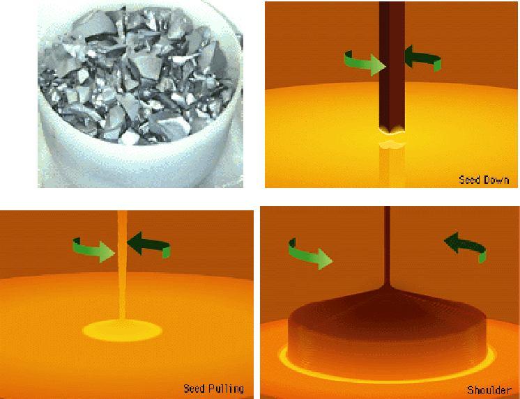
9 Polysilicon Ingots The polycrystalline silicon tubes refined by dissolving in hydrofluoric acid producing polysilicon ingots. Polycrystalline silicon has randomly oriented crystallites, electrical characteristics not ready for device fabrication. Must be transformed into single crystal silicon using crystal pulling MODULE-I IC TECHNOLOGY 9
10 Czochralski (CZ) crystal growing Step:1 Preparation of high purity molten silicon Step:2 Dipping Seed crystal Step:3 Pulling the seed upwards MODULE-I IC TECHNOLOGY 10
11 Czochralski (CZ) crystal growing All Si wafers come from Czochralski grown crystals. Polysilicon is melted, then held just below 1417 C, and a single crystal seed starts the growth. Pull rate, melt temperature and rotation rate control the growth It contains < 1 ppb impurities. Pulled crystals contain O (~10 18 cm -3 ) and C (~10 16 cm -3 ), plus dopants placed in the melt. MODULE-I IC TECHNOLOGY 11
12
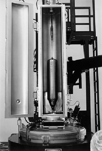
13 Silicon Ingot Grown by CZ Method Photograph courtesy of Kayex Corp., 300 mm Si ingot Photo 4.1
14

15 Examples of completed ingots
 and 400mm (16\") diameter ingots are being developed.")
16 Ingot Sizes Most ingots produced today are 150mm (6") and 200mm (8") diameter, For the most current technology 300mm (12") and 400mm (16") diameter ingots are being developed.
17 Ingot Characterization Single Crystal Silicon ingots are characterized by the orientation of their silicon crystals. Before the ingot is cut into wafers, one or two "flats" are ground into the diameter of the ingot to mark this orientation.
18 Crystal growth Obtaining sand Raw Polysilicon Czochralski Process (growing single crystal ingots) Ingot size and Characterization Wafer Fabrication Slicing Ingots Primary and Secondary Flats ( Orientation) Wafer Lapping Wafer Etching Wafer Polishing Wafer Cleaning MODULE-I IC TECHNOLOGY 18

19 Slicing Ingots The ingot is ground into the correct diameter for the wafers. Then it is sliced into very thin wafers. This is usually done with a diamond saw. MODULE-I IC TECHNOLOGY 19

20 Some wafers in storage trays MODULE-I IC TECHNOLOGY 20
21 Lattice Orientation The lattice orientation refers to the organized pattern of the silicon crystals in the wafer and their orientation to the surface. The orientation is obtained based on the orientation of the crystal that is placed into the molten silicon bath. The different orientations have different benefits and are used in different types of chips.
22 <100> Lattice Orientation This lattice orientation is used for MOS (metaloxide semiconductor), Bi-CMOS, & GaAs types of chips.
23 <111> Lattice Orientation This orientation is used for Bipolar types of chips
24 Different flats for orientation Wafer Flats - orientation for automatic equipment and indicate type and orientation of crystal. Primary flat The flat of longest length located in the circumference of the wafer. The primary flat has a specific crystal orientation relative to the wafer surface; major flat. Secondary flat Indicates the crystal orientation and doping of the wafer. MODULE-I IC TECHNOLOGY 24

25 Wafer Lapping The sliced wafers are mechanically lapped using a counter-rotating lapping machine and aluminum oxide slurry. This flattens the wafer surfaces, makes them parallel and reduces mechanical defects like saw markings MODULE-I IC TECHNOLOGY 25

26 Wafer Lapping Machine MODULE-I IC TECHNOLOGY 26
27 Wafer Etching After lapping, wafers are etched in a solution of nitric acid/ acetic acid or sodium hydroxide to remove microscopic cracks or surface damage created by the lapping process. The acid or caustic solution is removed by a series of high-purity RO/DI water baths MODULE-I IC TECHNOLOGY 27

28 Wafer polishing Next, the wafers are polished in a series of combination chemical and mechanical polish processes called CMP The wafers are held in a hard ceramic chuck using either wax bond or vacuum and buffed with a slurry of silica powder, RO/DI water and sodium hydroxide MODULE-I IC TECHNOLOGY 28
29 Wafer Cleaning A. Solvent Removal 1. Immerse in boiling trichloroethylene (TCE) for 3 min. 2. Immerse in boiling acetone for 3 min. 3. Immerse in boiling methyl alcohol for 3min. 4. Wash in DI water for 3min. B. Removal of Residual Organic/Ionic Contamination 1. Immerse in a (5:1:1) solution of H 2 O NH 4 OH-H 2 O 2 ;heat solution to C and hold for 10min 2. Quench the solution under running DI water 1 min 3. Wash in DI Water for 5min. C. Hydrous Oxide Removal 1. Immerse in a (1:50) solution of HF-H2 O for 15 sec 2. Wash in running DI water with agitation for 30 seconds. D. Heavy metal clean 1. Immerse in a (6:1:1) solution of H 2 O-HCL-H 2 O 2 for 10 min at a temperature of C 2. Quench the solution under running DI water for 1 min. 3. Wash in running DI water for 20min. MODULE-I IC TECHNOLOGY 29
30 Wafer Dimensions & Attributes Diameter (mm) Thickness ( m) Area (cm 2 ) Weight (grams/lbs) Weight/25 Wafers (lbs) / / / / Table 4.3
31 Increase in Number of Chips on Larger Wafer Diameters (Assume large 1.5 x 1.5 cm microprocessors) 88 die 200-mm wafer 232 die 300-mm wafer Figure 4.13
32 Developmental Specifications for 300-mm Wafer Dimensions and Orientation Parameter Units Nominal Some Typical Tolerances Diameter mm Thickness (center point) Warp (max) m 100 Nine-Point Thickness Variation (max) m m 10 Notch Depth mm , Notch Angle Degree 90 +5, -1 Back Surface Finish Edge Profile Surface Finish FQA (Fixed Quality Area radius permitted on the wafer surface) Bright Etched/Polished Polished mm 147 From H. Huff, R. Foodall, R. Nilson, and S. Griffiths, Thermal Processing Issues for 300-mm Silicon Wafers: Challenges and Opportunities, ULSI Science and Technology (New Jersey: The Electrochemical Society, 1997), p Table 4.4
33 Quality Measures Physical dimensions Flatness Microroughness Oxygen content Crystal defects Particles Bulk resistivity
CL 240: Materials Technology
 CL 240: Materials Technology Semiconductor materials Instructor: Vinay Prasad Materials and processing - descriptive, few mathematical equations Semiconductors (Si), dopants, metals, insulators 34% of
Physics and Material Science of Semiconductor Nanostructures
 Physics and Material Science of Semiconductor Nanostructures PHYS 570P Prof. Oana Malis Email: omalis@purdue.edu Today Bulk semiconductor growth Single crystal techniques Nanostructure fabrication Epitaxial
Chapter 2 Crystal Growth and Wafer Preparation
 Chapter 2 Crystal Growth and Wafer Preparation Professor Paul K. Chu Advantages of Si over Ge Si has a larger bandgap (1.1 ev for Si versus 0.66 ev for Ge) Si devices can operate at a higher temperature
Fabrication Process. Crystal Growth Doping Deposition Patterning Lithography Oxidation Ion Implementation CONCORDIA VLSI DESIGN LAB
 Fabrication Process Crystal Growth Doping Deposition Patterning Lithography Oxidation Ion Implementation 1 Fabrication- CMOS Process Starting Material Preparation 1. Produce Metallurgical Grade Silicon
The lowest quality of silicon is the so- called metallurgical silicon. The source material of making metallurgical silicon is quartzite.
 ET3034TUx - 4.2 - Manufacturing of crystalline silicon We have various types of silicon wafers such as monocrystalline silicon and polycrystalline silicon. In this block I will give an answer to the question:
The Physical Structure (NMOS)
") The Physical Structure (NMOS) Al SiO2 Field Oxide Gate oxide S n+ Polysilicon Gate Al SiO2 SiO2 D n+ L channel P Substrate Field Oxide contact Metal (S) n+ (G) L W n+ (D) Poly 1 3D Perspective 2 3 Fabrication
The Physical Structure (NMOS) Al SiO2 Field Oxide Gate oxide S n+ Polysilicon Gate Al SiO2 SiO2 D n+ L channel P Substrate Field Oxide contact Metal (S) n+ (G) L W n+ (D) Poly 1 3D Perspective 2 3 Fabrication
Lecture 2 Silicon Properties and Growth
 Lecture 2 Silicon Properties and Growth Chapters 1 & 2 Wolf and Tauber 1/63 Lecture 2 Why Silicon? Crystal Structure. Defects. Sand to Electronic Grade Polysilicon. Polycrystalline to Single Crystal Silicon.
PY2N20 Material Properties and Phase Diagrams
 PY2N20 Material Properties and Phase Diagrams Lecture 9 P. Stamenov, PhD School of Physics, TCD PY2N20-9 Semiconductor Wafer Production - Si Czochralski Growth Growth from melt Melt 99.999999% pure polycrystalline
Fabrication Technology
 Fabrication Technology By B.G.Balagangadhar Department of Electronics and Communication Ghousia College of Engineering, Ramanagaram 1 OUTLINE Introduction Why Silicon The purity of Silicon Czochralski
Semiconductor device fabrication
 REVIEW Semiconductor device fabrication is the process used to create the integrated circuits (silicon chips) that are present in everyday electrical and electronic devices. It is a multiplestep sequence
Silicon for Wafer production
 Silicon for Wafer production Introduction Production of Silicon Silicon is used in the semiconductor industry as raw material for the production of integrated circuits and solar cells. Integrated circuits
Microelettronica. Planar Technology for Silicon Integrated Circuits Fabrication. 26/02/2017 A. Neviani - Microelettronica
 Microelettronica Planar Technology for Silicon Integrated Circuits Fabrication 26/02/2017 A. Neviani - Microelettronica Introduction Simplified crosssection of an nmosfet and a pmosfet Simplified crosssection
Solar Photovoltaic Technologies
 Solar Photovoltaic Technologies Lecture-29 Prof. C.S. Solanki Energy Systems Engineering IIT Bombay Contents Brief summary of the previous lecture Production of Si MG-Si, EG-Si Siemens Process, FBR process
CRYSTAL GROWTH, WAFER FABRICATION AND BASIC PROPERTIES OF Si WAFERS- Chapter 3. Crystal Structure z a
 CRYSTAL GROWTH, WAFER FABRICATION AND BASIC PROPERTIES OF Si WAFERS- Chapter 3 Crystal Growth, Si Wafers- Chapter 3 z a C y B z a y Crystal Structure z a y Crystals are characterized by a unit cell which
VLSI Design and Simulation
 VLSI Design and Simulation CMOS Processing Technology Topics CMOS Processing Technology Semiconductor Processing How do we make a transistor? Fabrication Process Wafer Processing Silicon single crystal
KGC SCIENTIFIC Making of a Chip
 KGC SCIENTIFIC www.kgcscientific.com Making of a Chip FROM THE SAND TO THE PACKAGE, A DIAGRAM TO UNDERSTAND HOW CPU IS MADE? Sand CPU CHAIN ANALYSIS OF SEMICONDUCTOR Material for manufacturing process
EE CRYSTAL GROWTH, WAFER FABRICATION AND BASIC PROPERTIES OF Si WAFERS- Chapter 3. Crystal Structure z a
 1 EE 1 FALL 1999-00 CRYSTAL GROWTH, WAFER FABRICATION AND BASIC PROPERTIES OF Si WAFERS- Chapter 3 z a B Crystal Structure z a z a C y y y A x x Cubic BCC FCC x Crystals are characterized by a unit cell
Figure 2.3 (cont., p. 60) (e) Block diagram of Pentium 4 processor with 42 million transistors (2000). [Courtesy Intel Corporation.
 (e) Block diagram of Pentium 4 processor with 42 million transistors (2000). [Courtesy Intel Corporation.") Figure 2.1 (p. 58) Basic fabrication steps in the silicon planar process: (a) oxide formation, (b) selective oxide removal, (c) deposition of dopant atoms on wafer, (d) diffusion of dopant atoms into exposed
Figure 2.1 (p. 58) Basic fabrication steps in the silicon planar process: (a) oxide formation, (b) selective oxide removal, (c) deposition of dopant atoms on wafer, (d) diffusion of dopant atoms into exposed
H. Aülich PV Silicon AG Erfurt, Germany
 Workshop on "Physics for Renewable Energy" October 17-29, 2005 301/1679-28 "Technology of Solar-grade Silicon" H. Aülich PV Silicon AG Erfurt, Germany Silicon for the PV Industry Hubert A. Aulich PV Crystalox
Chapter 3 CMOS processing technology
 Chapter 3 CMOS processing technology (How to make a CMOS?) Si + impurity acceptors(p-type) donors (n-type) p-type + n-type => pn junction (I-V) 3.1.1 (Wafer) Wafer = A disk of silicon (0.25 mm - 1 mm thick),
Fabrication and Layout
 ECEN454 Digital Integrated Circuit Design Fabrication and Layout ECEN 454 3.1 A Glimpse at MOS Device Polysilicon Aluminum ECEN 475 4.2 1 Material Classification Insulators Glass, diamond, silicon oxide
Czochralski Crystal Growth
 Czochralski Crystal Growth Crystal Pulling Crystal Ingots Shaping and Polishing 300 mm wafer 1 2 Advantage of larger diameter wafers Wafer area larger Chip area larger 3 4 Large-Diameter Wafer Handling
Microelectronics. Integrated circuits. Introduction to the IC technology M.Rencz 11 September, Expected decrease in line width
 Microelectronics Introduction to the IC technology M.Rencz 11 September, 2002 9/16/02 1/37 Integrated circuits Development is controlled by the roadmaps. Self-fulfilling predictions for the tendencies
Low Power VLSI Circuits and Systems Prof. Ajit Pal Department of Computer Science and Engineering Indian Institute of Technology, Kharagpur
 Low Power VLSI Circuits and Systems Prof. Ajit Pal Department of Computer Science and Engineering Indian Institute of Technology, Kharagpur Lecture No. # 02 MOS Transistors - I Hello and welcome to today
VLSI Digital Systems Design
 VLSI Digital Systems Design CMOS Processing cmpe222_03process_ppt.ppt 1 Si Purification Chemical purification of Si Zone refined Induction furnace Si ingot melted in localized zone Molten zone moved from
Silicon Manufacturing
 Silicon Manufacturing Group Members Young Soon Song Nghia Nguyen Kei Wong Eyad Fanous Hanna Kim Steven Hsu th Fundamental Processing Steps 1.Silicon Manufacturing a) Czochralski method. b) Wafer Manufacturing
Chapter 2 MOS Fabrication Technology
 Chapter 2 MOS Fabrication Technology Abstract This chapter is concerned with the fabrication of metal oxide semiconductor (MOS) technology. Various processes such as wafer fabrication, oxidation, mask
EE 5611 Introduction to Microelectronic Technologies Fall Tuesday, September 02, 2014 Lecture 01
 EE 5611 Introduction to Microelectronic Technologies Fall 2014 Tuesday, September 02, 2014 Lecture 01 1 Instructor: Jing Bai Contact Email: jingbai@d.umn.edu, hone: (218)726-8606, Office: MWAH 255 Webpage:
Instructor: Dr. M. Razaghi. Silicon Oxidation
 SILICON OXIDATION Silicon Oxidation Many different kinds of thin films are used to fabricate discrete devices and integrated circuits. Including: Thermal oxides Dielectric layers Polycrystalline silicon
LANDOLT-BÖRNSTEIN. Zahlenwerte und Funktionen aus Naturwissenschaften und Technik. Neue Serie. Gesamtherausgabe: K.-H. Hellwege O.
 LANDOLT-BÖRNSTEIN Zahlenwerte und Funktionen aus Naturwissenschaften und Technik Neue Serie Gesamtherausgabe: K.-H. Hellwege O. Madelung Gruppe III: Kristall- und Festkörperphysik Band 17 Halbleiter Herausgeber:
INTEGRATED-CIRCUIT TECHNOLOGY
 INTEGRATED-CIRCUIT TECHNOLOGY 0. Silicon crystal growth and wafer preparation 1. Processing Steps 1.1. Photolitography 1.2. Oxidation 1.3. Layer Deposition 1.4. Etching 1.5. Diffusion 1.6 Backend: assembly,
Chapter 2 Manufacturing Process
 Digital Integrated Circuits A Design Perspective Chapter 2 Manufacturing Process 1 CMOS Process 2 CMOS Process (n-well) Both NMOS and PMOS must be built in the same silicon material. PMOS in n-well NMOS
CS/ECE 5710/6710. N-type Transistor. N-type from the top. Diffusion Mask. Polysilicon Mask. CMOS Processing
 CS/ECE 5710/6710 CMOS Processing Addison-Wesley N-type Transistor D G +Vgs + Vds S N-type from the top i electrons - Diffusion Mask Mask for just the diffused regions Top view shows patterns that make
Mostafa Soliman, Ph.D. May 5 th 2014
 Mostafa Soliman, Ph.D. May 5 th 2014 Mostafa Soliman, Ph.D. 1 Basic MEMS Processes Front-End Processes Back-End Processes 2 Mostafa Soliman, Ph.D. Wafers Deposition Lithography Etch Chips 1- Si Substrate
EE 5611 Introduction to Microelectronic Technologies Fall Tuesday, September 04, 2012 Lecture 01
 EE 5611 Introduction to Microelectronic Technologies Fall 2012 Tuesday, September 04, 2012 Lecture 01 1 Instructor: Jing Bai Contact Email: jingbai@d.umn.edu, hone: (218)726-8606, Office: MWAH 255 Webpage:
This Appendix discusses the main IC fabrication processes.
 IC Fabrication B B.1 Introduction This Appendix discusses the main IC fabrication processes. B.2 NMOS fabrication NMOS transistors are formed in a p-type substrate. The NMOS fabrication process requires
Chapter 1.6. Polished Single-Crystal Silicon, Prime Wafers (all numbers nominal) Wafer Specification Table. Diameter 100 mm 4-inch 150 mm 6-inch
 Wafer Specification Table. Diameter 100 mm 4-inch 150 mm 6-inch") Chapter 1.6 I - Substrate Specifications Polished Single-Crystal Silicon, Prime Wafers (all numbers nominal) Wafer Specification Table Diameter 100 mm 4-inch 150 mm 6-inch Thickness 525 µm 20.5 mils 675
Chapter 1.6 I - Substrate Specifications Polished Single-Crystal Silicon, Prime Wafers (all numbers nominal) Wafer Specification Table Diameter 100 mm 4-inch 150 mm 6-inch Thickness 525 µm 20.5 mils 675
CHAPTER - 4 CMOS PROCESSING TECHNOLOGY
 CHAPTER - 4 CMOS PROCESSING TECHNOLOGY Samir kamal Spring 2018 4.1 CHAPTER OBJECTIVES 1. Introduce the CMOS designer to the technology that is responsible for the semiconductor devices that might be designed
VLSI INTRODUCTION P.VIDYA SAGAR ( ASSOCIATE PROFESSOR) Department of Electronics and Communication Engineering, VBIT
 Department of Electronics and Communication Engineering, VBIT") VLSI INTRODUCTION P.VIDYA SAGAR ( ASSOCIATE PROFESSOR) contents UNIT I INTRODUCTION: Introduction to IC Technology MOS, PMOS, NMOS, CMOS & BiCMOS technologies. BASIC ELECTRICAL PROPERTIES : Basic Electrical
VLSI INTRODUCTION P.VIDYA SAGAR ( ASSOCIATE PROFESSOR) contents UNIT I INTRODUCTION: Introduction to IC Technology MOS, PMOS, NMOS, CMOS & BiCMOS technologies. BASIC ELECTRICAL PROPERTIES : Basic Electrical
PROCESSING OF INTEGRATED CIRCUITS
 PROCESSING OF INTEGRATED CIRCUITS Overview of IC Processing (Part I) Silicon Processing Lithography Layer Processes Use in IC Fabrication (Part II) Integrating the Fabrication Steps IC Packaging (Part
Photovoltaics: BASICS
 Laurea Magistrale in Scienza dei Materiali Materiali Inorganici Funzionali Photovoltaics: BASICS Prof. Antonella Glisenti - Dip. Scienze Chimiche - Università degli Studi di Padova AIR MASS NUMBER defines
CMOS Fabrication. Dr. Bassam Jamil. Adopted from slides of the textbook
 CMOS Fabrication Dr. Bassam Jamil Adopted from slides of the textbook CMOS Fabrication CMOS transistors are fabricated on silicon wafer Lithography process similar to printing press On each step, different
Silicon Wafers: Basic unit Silicon Wafers Basic processing unit 100, 150, 200, 300, 450 mm disk, mm thick Current industrial standard 300 mm
 Silicon Wafers: Basic unit Silicon Wafers Basic processing unit 100, 150, 200, 300, 450 mm disk, 0.5-0.8 mm thick Current industrial standard 300 mm (12 inches) Most research labs 100, 150 mm wafers (ours
VLSI Technology. By: Ajay Kumar Gautam
 By: Ajay Kumar Gautam Introduction to VLSI Technology, Crystal Growth, Oxidation, Epitaxial Process, Diffusion Process, Ion Implantation, Lithography, Etching, Metallization, VLSI Process Integration,
Wafer (1A) Young Won Lim 4/30/13
 Young Won Lim 4/30/13") Copyright (c) 2011-2013 Young W. Lim. Permission is granted to copy, distribute and/or modify this document under the terms of the GNU Free Documentation License, Version 1.2 or any later version published
Copyright (c) 2011-2013 Young W. Lim. Permission is granted to copy, distribute and/or modify this document under the terms of the GNU Free Documentation License, Version 1.2 or any later version published
Chapter 3 Silicon Device Fabrication Technology
 Chapter 3 Silicon Device Fabrication Technology Over 10 15 transistors (or 100,000 for every person in the world) are manufactured every year. VLSI (Very Large Scale Integration) ULSI (Ultra Large Scale
ELEC 3908, Physical Electronics, Lecture 4. Basic Integrated Circuit Processing
 ELEC 3908, Physical Electronics, Lecture 4 Basic Integrated Circuit Processing Lecture Outline Details of the physical structure of devices will be very important in developing models for electrical behavior
Thermal Oxidation and Growth of Insulators (Chapter 3 - Jaeger 3) Key advantage of Si: Oxidation of Si into SiO 2 (glass) Major factor in making
 Key advantage of Si: Oxidation of Si into SiO 2 (glass) Major factor in making") Thermal Oxidation and Growth of Insulators (Chapter 3 - Jaeger 3) Key advantage of Si: Oxidation of Si into SiO (glass) Major factor in making Silicon the main semiconductor Grown at high temperature in
Thermal Oxidation and Growth of Insulators (Chapter 3 - Jaeger 3) Key advantage of Si: Oxidation of Si into SiO (glass) Major factor in making Silicon the main semiconductor Grown at high temperature in
Introduction to CMOS VLSI Design. Layout, Fabrication, and Elementary Logic Design
 Introduction to CMOS VLSI Design Layout, Fabrication, and Elementary Logic Design CMOS Fabrication CMOS transistors are fabricated on silicon wafer Lithography process similar to printing press On each
A trip inside a microchip: a sand grain with a big memory
 A trip inside a microchip: a sand grain with a big memory Francesca di Monte, Associazione Culturale Chimicare francescadimonte@hotmail.com Prior to 1971, a computer unit was a huge machine, requiring
MATERIALS. Silicon Wafers... J 04 J 01. MATERIALS / Inorganics & thin films guide
 J MATERIALS SUBSTRATES Silicon Wafers... J 04 J J 01 MATERIALS SUBSTRATES NEYCO has a complete range of crystal substrates for a wide variety of applications, including Semiconductor, Biotechnology, Nanotechnology,
Making of a Chip Illustrations
 Making of a Chip Illustrations 22nm 3D/Trigate Transistors Version April 2015 1 The illustrations on the following foils are low resolution images that visually support the explanations of the individual
Radiation Tolerant Isolation Technology
 Radiation Tolerant Isolation Technology Background The following contains a brief description of isolation technologies used for radiation hardened integrated circuits. The technologies mentioned are junction
Crystalline Silicon Solar Cells
 12 Crystalline Silicon Solar Cells As we already discussed in Chapter 6, most semiconductor materials have a crystalline lattice structure. As a starting point for our discussion on crystalline silicon
Silicon VLSI Technology. Fundamentals, Practice and Modeling
 Text Book: Silicon VLSI Technology Fundamentals, Practice and Modeling Authors: J. D. Plummer, M. D. Deal, and P. B. Griffin Crystal Growth, Wafer Fab and Properties High Quality Single Crystal Wafers
EE6303 LINEAR INTEGRATED CIRCUITS AND APPLICATIONS 2 MARK QUESTIONS WITH ANSWERS UNIT I IC FABRICATION
 SRI VENKATESWARA COLLEGE OF ENGINEERING AND TECHNOLOGY TIRUPACHUR DEPARTMENT OFELECTRICAL AND ELECTRONICS ENGINEERING EE6303 LINEAR INTEGRATED CIRCUITS AND APPLICATIONS 1. Define an Integrated circuit.
Chapter 5 Thermal Processes
 Chapter 5 Thermal Processes 1 Topics Introduction Hardware Oxidation Diffusion Annealing Post-Implantation Alloying Reflow High Temp CVD Epi Poly Silicon Nitride RTP RTA RTP Future Trends 2 Definition
Lecture 19 Microfabrication 4/1/03 Prof. Andy Neureuther
 EECS 40 Spring 2003 Lecture 19 Microfabrication 4/1/03 Prof. ndy Neureuther How are Integrated Circuits made? Silicon wafers Oxide formation by growth or deposition Other films Pattern transfer by lithography
HOMEWORK 4 and 5. March 15, Homework is due on Monday March 30, 2009 in Class. Answer the following questions from the Course Textbook:
 HOMEWORK 4 and 5 March 15, 2009 Homework is due on Monday March 30, 2009 in Class. Chapter 7 Answer the following questions from the Course Textbook: 7.2, 7.3, 7.4, 7.5, 7.6*, 7.7, 7.9*, 7.10*, 7.16, 7.17*,
Microstructure of Electronic Materials. Amorphous materials. Single-Crystal Material. Professor N Cheung, U.C. Berkeley
 Microstructure of Electronic Materials Amorphous materials Single-Crystal Material 1 The Si Atom The Si Crystal diamond structure High-performance semiconductor devices require defect-free crystals 2 Crystallographic
Temperature Scales. Questions. Temperature Conversions 7/21/2010. EE580 Solar Cells Todd J. Kaiser. Thermally Activated Processes
 7/1/010 EE80 Solar Cells Todd J. Kaiser Flow of Wafer in Fabrication Lecture 0 Microfabrication A combination of Applied Chemistry, Physics and ptics Thermal Processes Diffusion & xidation Photolithograpy
KOREA UNIVERSITY. Ch. 4 Basics of device fabrication Reference: S. M. Sze, Semiconductor Devices, ISBN Photonics Laboratory
 Ch. 4 Basics of device fabrication Reference: S.. Sze, Semiconductor Devices, ISBN -471-8744-8 : We will understand the common techniques for growing single crystals. (a) The starting materials (e.g.,
Ajay Kumar Gautam [VLSI TECHNOLOGY] VLSI Technology for 3RD Year ECE/EEE Uttarakhand Technical University
![Ajay Kumar Gautam [VLSI TECHNOLOGY] VLSI Technology for 3RD Year ECE/EEE Uttarakhand Technical University](/thumbs/75/72824557.jpg "Ajay Kumar Gautam [VLSI TECHNOLOGY] VLSI Technology for 3RD Year ECE/EEE Uttarakhand Technical University") 2014 Ajay Kumar Gautam [VLSI TECHNOLOGY] VLSI Technology for 3RD Year ECE/EEE Uttarakhand Technical University Page1 Syllabus UNIT 1 Introduction to VLSI Technology: Classification of ICs, Scale of integration,
2014 Ajay Kumar Gautam [VLSI TECHNOLOGY] VLSI Technology for 3RD Year ECE/EEE Uttarakhand Technical University Page1 Syllabus UNIT 1 Introduction to VLSI Technology: Classification of ICs, Scale of integration,
EE40 Lec 22. IC Fabrication Technology. Prof. Nathan Cheung 11/19/2009
 Suggested Reading EE40 Lec 22 IC Fabrication Technology Prof. Nathan Cheung 11/19/2009 300mm Fab Tour http://www-03.ibm.com/technology/manufacturing/technology_tour_300mm_foundry.html Overview of IC Technology
BASICS OF MANUFACTURING INTEGRATED CIRCUITS
 BASICS OF MANUFACTURING INTEGRATED CIRCUITS Opportunities for filtration exist for the manufacture of very small electronic components referred to as semiconductors. This broad category includes devices
Microelectronics Devices
 Microelectronics Devices Yao-Joe Yang 1 Outline Basic semiconductor physics Semiconductor devices Resistors Capacitors P-N diodes BJT/MOSFET 2 Type of Solid Materials Solid materials may be classified
Lecture 0: Introduction
 Lecture 0: Introduction Introduction Integrated circuits: many transistors on one chip. Very Large Scale Integration (VLSI): bucketloads! Complementary Metal Oxide Semiconductor Fast, cheap, low power
A discussion of crystal growth, lithography, etching, doping, and device structures is presented in
 Chapter 5 PROCESSING OF DEVICES A discussion of crystal growth, lithography, etching, doping, and device structures is presented in the following overview gures. SEMICONDUCTOR DEVICE PROCESSING: AN OVERVIEW
CHAPTER 1 HOW SEMICONDUCTOR CHIPS ARE MADE
 CHAPTER 1 HOW SEMICONDUCTOR CHIPS ARE MADE Hwaiyu Geng Hewlett-Packard Company Palo Alto, California Lin Zhou Intel Corporation Hillsboro, Oregon 1.1 INTRODUCTION Over the past decades, an information
Lecture 22: Integrated circuit fabrication
 Lecture 22: Integrated circuit fabrication Contents 1 Introduction 1 2 Layering 4 3 Patterning 7 4 Doping 8 4.1 Thermal diffusion......................... 10 4.2 Ion implantation.........................
Microfabrication of Integrated Circuits
 Microfabrication of Integrated Circuits OUTLINE History Basic Processes Implant; Oxidation; Photolithography; Masks Layout and Process Flow Device Cross Section Evolution Lecture 38, 12/05/05 Reading This
Complexity of IC Metallization. Early 21 st Century IC Technology
 EECS 42 Introduction to Digital Electronics Lecture # 25 Microfabrication Handout of This Lecture. Today: how are Integrated Circuits made? Silicon wafers Oxide formation by growth or deposition Other
EELE408 Photovoltaics Lecture 02: Silicon Processing
 EELE408 Photovoltaics Lecture 0: licon Processing Dr. Todd J. Kaiser tjkaiser@ece.montana.edu Department of Electrical and Computer Engineering Montana State University - Bozeman The Fabrication Process
EECS130 Integrated Circuit Devices
 EECS130 Integrated Circuit Devices Professor Ali Javey 9/13/2007 Fabrication Technology Lecture 1 Silicon Device Fabrication Technology Over 10 15 transistors (or 100,000 for every person in the world)
EE 330 Lecture 9. IC Fabrication Technology Part II. -Oxidation -Epitaxy -Polysilicon -Planarization -Resistance and Capacitance in Interconnects
 EE 330 Lecture 9 IC Fabrication Technology Part II -Oxidation -Epitaxy -Polysilicon -Planarization -Resistance and Capacitance in Interconnects Review from Last Time Etching Dry etch (anisotropic) SiO
EFFECT OF CRYSTALORIENTATIONIN OXIDATION PROCESS OF VLSI FABRICATION
 International Journal of Research in Engineering, Technology and Science, Volume VII, Special Issue, Feb 2017 www.ijrets.com, editor@ijrets.com, ISSN 2454-1915 EFFECT OF CRYSTALORIENTATIONIN OXIDATION
IC/MEMS Fabrication - Outline. Fabrication
 IC/MEMS Fabrication - Outline Fabrication overview Materials Wafer fabrication The Cycle: Deposition Lithography Etching Fabrication IC Fabrication Deposition Spin Casting PVD physical vapor deposition
Micromachining vs. Soft Fabrication
 Introduction to BioMEMS & Medical Microdevices Silicon Microfabrication Part 1 Companion lecture to the textbook: Fundamentals of BioMEMS and Medical Microdevices, by Prof., http://saliterman.umn.edu/
Bulk crystal growth. A reduction in Lg will increase g m and f oper but with some costs
 Bulk crystal growth The progress of solid state device technology has depended not only on the development of device concepts but also on the improvement of materials. A reduction in Lg will increase g
Why silicon? Silicon oxide
 Oxidation Layering. Oxidation layering produces a thin layer of silicon dioxide, or oxide, on the substrate by exposing the wafer to a mixture of highpurity oxygen or water at ca. 1000 C (1800 F). Why
Lecture #18 Fabrication OUTLINE
 Transistors on a Chip Lecture #18 Fabrication OUTLINE IC Fabrication Technology Introduction the task at hand Doping Oxidation Thin-film deposition Lithography Etch Lithography trends Plasma processing
Semiconductor Grade Silicon *
 OpenStax-CNX module: m31994 1 Semiconductor Grade Silicon * Andrew R. Barron Based on Synthesis and Purication of Bulk Semiconductors by Carissa Smith Andrew R. Barron This work is produced by OpenStax-CNX
Monocrystalline Silicon Wafer Specification (Off-spec)
") Monocrystalline Silicon Wafer Specification (Off-spec) General information: o Product: Wafer o Code: n-125-166f-f180µ o Version date: 2011-10-06 Key characteristics: o Czochralski grown o n-type o 125.25
Monocrystalline Silicon Wafer Specification (Off-spec) General information: o Product: Wafer o Code: n-125-166f-f180µ o Version date: 2011-10-06 Key characteristics: o Czochralski grown o n-type o 125.25
PHYS 534 (Fall 2008) Process Integration OUTLINE. Examples of PROCESS FLOW SEQUENCES. >Surface-Micromachined Beam
 Process Integration OUTLINE. Examples of PROCESS FLOW SEQUENCES. >Surface-Micromachined Beam") PHYS 534 (Fall 2008) Process Integration Srikar Vengallatore, McGill University 1 OUTLINE Examples of PROCESS FLOW SEQUENCES >Semiconductor diode >Surface-Micromachined Beam Critical Issues in Process
PHYS 534 (Fall 2008) Process Integration Srikar Vengallatore, McGill University 1 OUTLINE Examples of PROCESS FLOW SEQUENCES >Semiconductor diode >Surface-Micromachined Beam Critical Issues in Process
CMOS FABRICATION. n WELL PROCESS
 CMOS FABRICATION n WELL PROCESS Step 1: Si Substrate Start with p- type substrate p substrate Step 2: Oxidation Exposing to high-purity oxygen and hydrogen at approx. 1000 o C in oxidation furnace SiO
Materials: Structures and Synthesis
 微纳光电子材料与器件工艺原理 Materials: Structures and Synthesis Xing Sheng 盛兴 Department of Electronic Engineering Tsinghua University xingsheng@tsinghua.edu.cn 1 Optical and Electronic Devices LEDs lasers waveguides
VLSI. Lecture 1. Jaeyong Chung System-on-Chips (SoC) Laboratory Incheon National University. Based on slides of David Money Harris
 Laboratory Incheon National University. Based on slides of David Money Harris") VLSI Lecture 1 Jaeyong Chung System-on-Chips (SoC) Laboratory Incheon National University Based on slides of David Money Harris Goals of This Course Learn the principles of VLSI design Learn to design
VLSI Lecture 1 Jaeyong Chung System-on-Chips (SoC) Laboratory Incheon National University Based on slides of David Money Harris Goals of This Course Learn the principles of VLSI design Learn to design
Mikrosensorer. Microfabrication 1
 Mikrosensorer Microfabrication 1 Literature Introductory MEMS Fabrication and Applications Thomas M. Adams and Richard A. Layton Available as ebook on http://www.lub.lu.se/en/search/lubsearch.html This
Microelectronic Device Instructional Laboratory. Table of Contents
 Introduction Process Overview Microelectronic Device Instructional Laboratory Introduction Description Flowchart MOSFET Development Process Description Process Steps Cleaning Solvent Cleaning Photo Lithography
FABRICATION OF CMOS INTEGRATED CIRCUITS. Dr. Mohammed M. Farag
 FABRICATION OF CMOS INTEGRATED CIRCUITS Dr. Mohammed M. Farag Outline Overview of CMOS Fabrication Processes The CMOS Fabrication Process Flow Design Rules EE 432 VLSI Modeling and Design 2 CMOS Fabrication
Chapter 4. UEEP2613 Microelectronic Fabrication. Oxidation
 Chapter 4 UEEP2613 Microelectronic Fabrication Oxidation Prepared by Dr. Lim Soo King 24 Jun 2012 Chapter 4...113 Oxidation...113 4.0 Introduction... 113 4.1 Chemistry of Silicon Dioxide Formation... 115
Graphite and C/C Products for Semiconductor & Solar Applications
 Graphite and C/C Products for Semiconductor & Solar Applications Graphite and C/C Products for Semiconductor & Solar Applications www.schunk-group.com SCHUNK GROUP HIGH TEMPERATURE APPLICATIONS Schunk
From sand to silicon wafer
 From sand to silicon wafer 25% of Earth surface is silicon Metallurgical grade silicon (MGS) Electronic grade silicon (EGS) Polycrystalline silicon (polysilicon) Single crystal Czochralski drawing Single
TOWARD MEMS!Instructor: Riadh W. Y. Habash
 TOWARD MEMS!Instructor: Riadh W. Y. Habash Students are presented with aspects of general production and manufacturing of integrated circuit (IC) products to enable them to better liaise with and participate
Sustainable Si production for solar cells a responsibility for Norway? (or how can Norway contribute to the PV industry in collaboration with China?
 Sustainable Si production for solar cells a responsibility for Norway? (or how can Norway contribute to the PV industry in collaboration with China?) Gabriella Tranell, Associate Professor The Norwegian
Fused-Salt Electrodeposition of Thin-Layer Silicon
 NREL/CP-450-22928 UC Category: 1250 Fused-Salt Electrodeposition of Thin-Layer Silicon J.T. Moore, T.H. Wang, M.J. Heben, K. Douglas, and T.F. Ciszek Presented at the 26th IEEE Photovoltaic Specialists