Bare Board Material Performance after Pb-Free Reflow
|
|
|
- Darleen Curtis
- 6 years ago
- Views:
Transcription
 consortia completed an extensive study of 29 different bare board material and stackup combinations and their associated performance after 6X Pb-free")
1 Bare Board Material Performance after Pb-Free Reflow Joe Smetana, Alcatel-Lucent Thilo Sack, Celestica Wayne Rothschild, IBM Bill Birch, PWB Interconnect Solutions Kim Morton, Viasystems Abstract: The High Density Packaging Users Group (HDPUG) consortia completed an extensive study of 29 different bare board material and stackup combinations and their associated performance after 6X Pb-free reflow at 260 C. Data presented will focus on the air-air thermal cycling, IST testing and material survivability after Pb-free assembly reflow portions of this testing. Test board design aspects, manufacturing processes, Weibull analysis, and failure analysis data will be presented. The impact of plated through hole pitch on laminate integrity and how material properties relate to the results will be discussed. 1 Overview This project was designed to look at a significant number of bare boards materials in different constructions in relation to Pbfree assembly reflow processing. Included in the test were both filled and unfilled FR4 materials from multiple major material manufacturers. Additionally, a limited number of high frequency/high speed materials and halogen free materials were evaluated. The project included 29 different materials/stackup combinations, 2 different layer counts, 2 different thicknesses, and 4 different resin contents. Results include, thermal analysis of the boards (TMA and DSC, Tg, CTE, Td, T260, T288, T300), visual inspection of the materials after 6X Pb-free reflow, IST testing (with and without reflow preconditioning) and failure analysis, air-air thermal cycling and associated failure analysis, limited CAF hole-wall to holewall analysis and electrical performance measurements (S-Parameter testing) resulting in the Dk and Df of the materials over frequency before and after reflow processing. This paper will focus on thermal cycling, IST, and material survivability results from this testing. 2 Printed Circuit Board Design Two different but very similar test board designs were used for this project; a 20 layer version and a 6 layer version. See Figure 1. Figure 1: Test Vehicle
 reliability in accelerated air to air thermal cycling (ATC).")
2 Figure 2: Different Test Sections Both versions of the board include the following sections as shown in Figure 2: Air-Air (ATC) section: This section includes 4 different sets of 8 nets each consisting of daisy chains of 50 through hole vias designed for in-situ monitoring of plated through hole (via) reliability in accelerated air to air thermal cycling (ATC). Each set has different hole sizes. There are 3 sets of daisy chain nets on inch centers. These are spaced widely enough that you can directly compare the thermal cycle performance of different materials, with minimal influence from adjacent vias and/or material degradation associated with tight hole pitches. One daisy chain set of holes has a drilled hole size prior to plating of.010 inches, one at inches prior to plating and a third set at inches prior to plating. The final set of daisy chain holes, also drilled at inches prior to plating, is on a 0.8mm pitch to represent a worst case via density typical of complex high I/O 0.8mm pitch BGA s routed with through hole vias. This enables direct comparison of the performance of widely spaced vias vs. vias at the smallest spacing used on actual boards. The tighter spaced holes are typically much more prone to thermal issues (delamination, eyebrow cracking, etc.) than the wider spaced holes. Daisy chains on the 20 layer version of the board go from layer 2 to layer 19, so that at any foil cracking or interconnect separation, should it occur, will be identified as a failure, in addition to the expected failure mode of barrel cracking. On the 6 layer version of the test vehicle, all the daisy chains go from layer 1 to layer 6. The holes are large enough that significant failures in these holes will typically represent a foil crack or interconnect separation failure mode. For this project only the inch hole sizes were tested. The affect of different hole sizes and associated aspect ratios was previously evaluated in the HDPUG Via Integrity project 2. Also for this test program, on the thicker boards (20 layer and thick 6 layer constructions), the inch hole sizes were actually drilled at inches to eliminate concerns with plating the associated high aspect ratio holes. The drill size limited the plated through hole aspect ratio to 10:1. In this section, internal pads are used on roughly one half of the internal layers to represent the worst case situation typically seen in real boards. Previous testing has shown that the presence of internal pads on plated through holes reduces the long term thermal cycle reliability of the plated through holes 1.
3 The ground returns are routed on multiple layers and near the center of the board such that they greatly reduce the potential for the attachment points (at a connector pattern) being the source of the failure rather than the via daisy chains themselves. Note that the connector pattern is designed for wiring directly to. Connectors are not inserted here to eliminate any chance of a connector failure impacting the results. IST section: This section consists of two IST (Interconnect Stress Test) coupons using a generic through hole coupon design. The P1 / S1 circuit is on a 1mm grid with.010 inch drilled vias and the P2 / S2 circuit is on a 2mm grid with combinations of inch and inch drilled vias. As with the ATC section, for this test program, on the thicker boards (20 layer and thick 6 layer constructions) the inch hole sizes were actually drilled at inches to eliminate concerns with plating of the associated high aspect ratio holes. Internal layer pads are used on all layers of the IST coupons. Also included in this section are capacitance test planes and associated test points. CAF section: This section is designed to for testing hole-wall to hole-wall conductive anodic filament (CAF) at two spacing s, inch hole-wall to hole-wall and inch hole-wall to hole-wall using a drilled hole size of inches prior to plating (Note the spacing was supposed to have been at 0.016, but a design error that was not caught until much later resulted in a inch spacing). The rather large hole size (compared to small vias) was chosen specifically to minimize any affects from drill wander or potentially poor hole wall quality associated with very small drill bit sizes such that the CAF performance of the materials would be evaluated minimizing the effect of the drilling process. Each of the two different hole-wall to hole-wall spacing s are designed in two axes such that both warp and fill of the materials would be evaluated. The design is such that the warp and fill directions are in the same nets and not separable by direction without further failure analysis. The spacing s were chosen such that failures during CAF testing were expected. The goal was to create failures such that the affect of Pb-free reflow on CAF performance, if any, would be seen. Additionally, the sample size, specifically the number of potential failure sites, was intentionally limited to 60 per board per hole-wall spacing to hopefully spread out the failures sufficiently in time to more readily see differences between materials. Electrical Test section: The electrical test section on the 20 layer version of the board consists of stripline traces on layer 2 between planes on layers 1 and 3 and microstrip traces on layer 1 referenced to a layer 2 plane. The internal stripline traces are connected by microvias to minimize and virtually eliminate the influence of the vias on the test results. This section is designed for S-parameter testing. On the 6 layer version, the stripline section does not exist and only microstrip traces are included. Although the test board is not designed with a separate section for evaluating the laminate integrity after reflow soldering, incorporated within the board design are plated through holes on inch centers (ATC section), 2mm pitch centers (IST section), 1mm pitch centers (IST section), and 0.8mm pitch centers (ATC section) enabling evaluation of the impact of PTH pitch on material performance after reflow (by cross-section). The board is physically 7 inches by 10 inches overall and the thickness is defined by the material stackup and construction as detailed following. The individual test sections are separable either by score lines or by breakaways so that they can be individually separated for testing. 2.1 Material Stack Ups The test boards are fabricated using 4 different stackups, two for the 20 layer construction and two for the 6 layer construction. All material types tested used identical stackups with the same glass style and resin content for each given stackup, regardless of material supplier. This way the materials can be directly compared to one another. For the 20 layer constructions, both the standard and high resin constructions are essentially identical in thickness at inches and inches thick respectively such that the effect of resin content can be evaluated independently of layer count and board thickness. The standard 20 layer construction has an overall resin content of 58% and is a typical construction for a 20 layer board of this thickness as shown in figure 3. The high resin content 20 layer construction has an overall resin content of 69% and represents very complex and worst case constructions that would typically have higher layer counts (such as 26 or 28 layers) in a similar thickness. This stackup is detailed in figure 4. The six layer construction is done in two different thicknesses. A thick construction at inches thick and 45% overall resin content (figure 5) and a thin construction at inches thick and 48% overall resin content (figure 6). The thick construction, with the same thickness as the 20 layer construction enables comparison of the same thickness with different layer counts. However, due to requirements inherent to the construction of thick low layer count boards, the thick 6-layer construction has a lower resin content confounding the effect of layers such that the effects of layer count and resin content cannot be completely separated.

4 Figure 3: 20 layer standard stackup, 58% resin content Figure 4: 20 layer high resin content stackup, 69% resin content Figure 5: Thick 6 layer stackup, 45% resin content

5 Figure 6: Thin 6 layer stackup, 48% resin content 2.2 PCB Surface Finish The PCB finish chosen for this testing was immersion silver. The actual finish used was not critical, provided it remained solderable after 6X reflow at 260ºC and did not include a nickel underlayer as a nickel underlayer would potentially affect many of the results 2,3. 3 Materials Material selection for this project required narrowing down a large set of potential materials to be tested into a manageable set. Two materials, filled and non-filled versions of a Phenolic FR4, were chosen as the baseline materials for comparison. Inputs from team members and material suppliers were considered. The primary focus of this testing on the 20 layer boards was high Tg materials that fell into the category of lower cost alternatives. Also tested were a limited number of high speed materials. All of these materials were tested with the standard construction. Four materials (2 filled and 2 unfilled) we tested with the high resin content construction. For the thin 6 layer boards, the focus was mid-tg FR4 materials and included a limited number of halogen free materials.
6 Materials selected and the associated stackups are shown below in table 1. Table 1: Materials and Stackups 20 Layer Materials and Constructions Code Material Type Stackup A Baseline Non-Filled Phenolic FR4 Standard B Baseline Filled Phenolic FR4 Standard C Filled Proprietary Resin FR4 Standard D Filled Phenolic FR4 Standard E Unfilled Phenolic FR4 Standard F Unfilled Phenolic FR4 Standard G Filled Phenolic FR4 Standard H Unfilled Phenolic FR4 Standard I Filled Phenolic FR4 Standard J Filled Phenolic FR4 Standard K Unfilled Phenolic FR4 Standard L Hi-Speed Material Standard M Hi-Speed Material Standard N Hi-Speed Material Standard P Unfilled Phenolic FR4 High Resin Q Filled Phenolic FR4 High Resin R Unfilled Phenolic FR4 High Resin S Filled Phenolic FR4 High Resin 6 Layer Materials and Constructions Code Material Stackup T Halogen Free FR4, Filled, Dicy, Mid Tg.062" Thick U Halogen Free FR4, Filled, Dicy, Hi Tg.062" Thick V Halogen Free FR4, Filled, Dicy, Hi Tg.062" Thick W Filled Phenolic FR4, Mid Tg.062" Thick X Halogen Free FR4, Filled, Dicy, Mid Tg.062" Thick Y Filled Phenolic FR4, Mid Tg.062" Thick Z Filled Phenolic FR4, Mid Tg.062" Thick AA Filled Phenolic FR4, Mid Tg.062" Thick BB Filled Phenolic FR4, Low Tg.062" Thick CC Unfilled Phenolic FR4, Hi Tg.116" Thick DD Filled Phenolic FR4, Hi Tg.116" Thick 4 PWB Fabrication Fabrication of the all the boards was done at Viasystems, China. To ensure a level playing field between materials, all materials were processed per material supplier recommendations and did not include any process modifications by Viasystems. Each material supplier was required to review and approve the fabrication process before their materials were fabricated. Each material was built with a trailblazer lot to ensure a viable process, followed by the main lot. Boards used for the testing came from the main lot. Fabrication of the boards occurred between November 2006 and June To minimize any variability in the plating process affecting the test results, each lot of material was built through lamination and then stored until all similar constructions were completed through the same step such that plating could be done in single plating run.
7 The process steps from lamination on are summarized as follows: 1. All the 20 layer and thick 6 layer lots were accumulated after lamination prior to drill until every material lot was laminated. 2. All lots were then drilled at the same time on 2 identical Hitachi Mark 20 drill machines only. 3. All lots were then went through the same PTH line (Rohm Haas (Shipley) C3000 series with high build) at the same time (Hi-speed materials got Plasma first and then joined the other lots) 4. All lots after PTH went immediately to Panel Plate (Rohm Haas (Shipley) EP-1000) at the same time 5. All lots were then printed and developed at the same time 6. All lots were then put on the same electroplater (Pattern plating line with Rohm Haas EP-1000 chemistry (7.5 ASF X 180 minutes)) within the center section using 4 cells only and run over approximately a 20 hr period. This electroplating bath had been carbon treated several days in advance to ensure the ductility of the copper. Just prior to putting all lots into the cells, the chemistry was analyzed and replenished as needed. Ductility samples were taken before and after the 20hr run of all lots (see below) and the order of plating for each lot was recorded (see details in the IST section of this report). Each lot was put on only one flight bar of eight panels The following are the ductility measurements before and after plating on the 20 layer and thick 6 layer plating run: Before: 29.5%, 28.4%, 29.8%, 29.3%, 29.0% After: 24%, 25.8%, 23%, 26.3%, 25.7% 7. All lots were then stripped and etched at the same time 8. Remaining processes such as Solder Mask and Surface Finish were then concluded with Kelvin testing of each lot for the 11.7 mil vias. No repair operations were allowed. The thin 6 layer lots followed and used the identical procedure as above. Thin 6 layer lots were plated separately from the 20 layer and 6 layer thick lots. 5 Testing The testing included thermal analysis (TMA and DSC), Visual Inspection, Air-Air thermal cycling, IST capacitance checks and cycling, CAF testing, and S-Parameter testing both before and after 6X reflow, plus extensive failure analysis cross sections. Contributors: Test Board Designs Materials Fabrication of Test Vehicles Thermal Analysis Reflow and Visual Inspection Air-Air thermal cycling IST Testing CAF Testing S-Parameter Testing Failure Analysis Alcatel-Lucent Material Suppliers for each material Viasystems Viasystems Celestica China Endicott Interconnect Technologies under contract from HDPUG PWB Interconnect Solutions Nelco (blind) Isola (blind) subcontracted to Microtek Labs Sun Microsystems Viasystems PWB Interconnect Solutions under contract from Sun Microsystems Figure 7 is a flow chart of the testing done. In general all boards followed the same flow. The S-Parameter testing was not done on the as-built thin 6 layer boards, and the air-air thermal cycling was limited to boards tested after reflow. IST capacitance testing was not done on the 6 layer boards. The board design has score lines and breakaway sections to allow the individual sections to be separated for the various tests to allow them to be tested in parallel.
 Failure")
8 Fabricate Boards As-Built Testing Reflow Boards Inspect as received and after reflows Thermal Analysis IST Analysis Capacitance IST Cycling Failure Analysis Thermal Analysis IST Analysis Capacitance IST Cycling Failure Analysis S-Parameter Testing CAF Testing S-Parameter Testing CAF Testing Figure 7: Flow Chart of Testing Air-Air ATC Testing (20 layer and thick 6 layer only) Failure Analysis 6 Board Pre-conditioning All boards were preconditioned at Celestica s Suzhou China facility. A BTU Pyramax150N 10 zone forced convection oven was used. Figure 8: Oven used for Preconditioning 6.1 Preconditioning Profile The following parameters were used to create the reflow profiles.

9 Table 3: Target Reflow Profile Parameters Profile Elements 10 Zone Convection Oven Recommended Ramp Rate to 217 C Peak Linear Ramp desired. Can have a small soak period. Usually 1 to 5 C/sec. No more than 2 C/sec Pre-heat Temperature Usually measured from 150 C to 200 C. Times within this temperature range are usually 60 to 120 seconds TAL (Time above 217 C Liquidus) Target 60 to 90 seconds Time within 5 C of max Peak temp. 10 to 20 seconds ok. Usually will be lower time. Target peak Temperature 260 C Minimum +5 C / -0 C Ramp Down Rate Target from 1.5 C/sec to 2.5 C/sec with normal oven cooling configuration Reflow Atmosphere Run all samples in air. (Worst case scenario) Total Time in Oven Thermocouples Attachment Usually 4 to 6 minutes Require minimum of 3 T/C s to properly profile raw card. (Leading Edge + Centre of Card +Trailing edge) are recommended locations. Profile cards were generated for each of the stackup configurations. A picture of where the thermocouples were attached to the profile cards is shown below in Figure 9. Figure 9: Profile Board Profiles were established for each of the 4 stackup combinations. Below are the resulting profiles used:


10 Figure 10: Profile for A-N - 20 Layer - Low Resin Content - Stackup A Figure 11: Profile for P-S - 20 Layer High Resin Content - Stackup B


11 Figure 12: Profile for T-BB - 6 Layer Stackup A Figure 13: Profile for CC-DD - 6 Layer Stackup B 6.2 Pre-conditioning Procedure Boards were not baked prior to reflow. Panels were taken out of the packaging material and used as received. Prior to the start of each pre-conditioning run, the profiles were verified again to validate that nothing had changed between when the profiles was generated and when the actual board pre-conditioning run took place. During the actual runs, the cards were introduced into the oven to guarantee a minimum board spacing of at least 2 zones. This was to ensure that there were no thermal interactions between cards. As well, each card was let to cool to room temperature before being reflowed again, to guarantee that each card experienced the same thermal excursion between profile runs.
12 Small labels with the numbers 1 to n were attached near each dash number box on each coupon on the panel. This was done to ensure traceability back the original panel once all the coupons were broken out of the panel at the end of the pre-conditioning. A tracking sheet was used to manually track and record all boards through the process. Prior to start of the preconditioning, a photograph was taken of one panel from each dash number. After all subsequent reflow cycles the panels were inspected for any defects. All defects were recorded in the tracking sheets and photographed noting the defect location, type and run number. After the completion of 3X and 6X reflow cycles, 1 panel from each dash number were photographed for comparison purposes to the incoming board condition. 6.3 Summary of Pre-conditioning Results The tables below provide a summary of the visually observed results after pre-conditioning. Dash Number Table 4: Summary of Results for 20 Layer PWB Laminates Material 20 Layer Constructions Stackup (A=Low Resin Content, B=High Resin Content) Results Baseline Non-Filled Phenolic Blistering/delamination after 4X reflow. A A FR4 Minor discoloration B Baseline Filled Phenolic FR4 A No defects C Filled Proprietary Resin FR4 A No defects D Filled Phenolic FR4 A No defects other than incoming A Minor blistering/delamination after 5X E Unfilled Phenolic FR4 reflow Minor blistering/delamination after 5X reflow F Unfilled Phenolic FR4 A G Filled Phenolic FR4 A No defects Major delamination and blistering after only 2X reflow H Unfilled Phenolic FR4 A I Filled Phenolic FR4 A No defects A Minor blistering/delamination after 3X reflow J Filled Phenolic FR4 K Unfilled Phenolic FR4 A No defects L Hi-Speed Material A No defects M Hi-Speed Material A No defects N Hi-Speed Material A No defects other than incoming Minor blistering/delamination after 6X reflow P Unfilled Phenolic FR4 B Q Filled Phenolic FR4 B No defects Major delamination and blistering after B R Unfilled Phenolic FR4 6X reflow S Filled Phenolic FR4 B No defects other than incoming
13 Dash Number Table 5: Summary of Results for 6 Layer PWB Laminates Material 6 Layer Constructions Stackup (A=.062 Thick, B=.116 Thick) Results Halogen Free FR4, Filled, Dicy, T Mid Tg A No defects Halogen Free FR4, Filled, Dicy, U Hi Tg A No defects Halogen Free FR4, Filled, Dicy, V Hi Tg A No defects W Filled Phenolic FR4, Mid Tg A No defects Halogen Free FR4, Filled, Dicy, X Mid Tg A No defects Y Filled Phenolic FR4, Mid Tg A No defects. Discoloration. Z Filled Phenolic FR4, Mid Tg A No defects. Discoloration. Severe blistering and delamination after only A AA Filled Phenolic FR4, Mid Tg 1X reflow. BB Filled Phenolic FR4, Low Tg A No defects. Discoloration. CC Unfilled Phenolic FR4, Hi Tg B No defects DD Filled Phenolic FR4, Hi Tg B No defects Of all the materials run, only Material R and Material AA exhibited severe signs of blistering / delamination during the preconditioning. 7 LAMINATE INTEGRITY AFTER PB-FREE REFLOW 7.1 Evaluation of Internal Laminate Integrity An important consideration for Pb-free materials, before any of the long-term reliability considerations are addressed is the survivability of the laminates without degradation after the Pb-free assembly process. Often the degradation of the material is internal and not visible to an external visual inspection, necessitating cross-sections Preparation and Inspection of Cross-sections Vertical cross-sections of vias were prepared from IST and ATC coupons of each material / thickness combination. All of the mounts taken from ATC coupons were prepared after the coupons were subjected to 6 passes of reflow simulation (peak temperature of 260 o C) by Celestica, followed by ATC testing (peak temperature of 125 o C). Mounts were taken from IST coupons as built, followed by IST testing (peak temperature of 150 o C); or after being subjected to 6x260 o C reflow simulation by Celestica. The latter were prepared as received (motivated by opens or high-resistance readings) or after IST testing. Prepared to view vias, the face of each mount was parallel to the x- or y-direction of the test vehicle. Magnification of 50x or higher was used. Photos were provided as appropriate. 7.2 Results Inspection of Cross-sections of Via Arrays Inspections of cross-sections of coupons that were subjected to reflow simulation revealed numerous instances of via-to-via pitch-dependent internal laminate structural defects. No signs of this damage were noted during Celestica s careful inspection of the outer surfaces of these coupons after reflow simulation. No signs of these internal defects were noted during inspection of cross-sections of IST coupons that were not subjected to reflow simulation. These laminate defects are classified as eyebrow cracks or as longitudinal cracks, both of which are described below.
14 It is important to remember that the field of view obtained from inspection of cross-sections is inherently limited. Although general trends are noted, it is assumed that further details could be obtained from further analyses of existing cross-sections and by preparation of additional cross-sections from the test parts. Eyebrow cracks (see Figure 14) were found at the outer periphery of some internal lands. These tend to occur at what appears to be the copper-to-resin interface along most of the vertical portion of the end of the internal land. These often extend for a short distance in a generally diagonal pathway above and/or below the unused land and/or may extend for a short distance along the horizontal interface between the land and the laminate. Figure 14 Longitudinal cracks (see Figure 15) extend horizontally (often completely or almost completely) between adjacent vias. These are seen in one or more layers within a given cross-section. These occur within layers that are within the middle third of the stack-up, with a predominance of these being near the center of the stack-up. The majority of cracks include at least some vertical component, sometimes following the sinusoidal pattern of the glass bundles. Besides being at the glass-to-resin interface, these may exist within the resin and/or at the copper-to-resin interface and/or at the core-to-prepreg interface. Figure 15
15 Table 6 lists what was reported as the predominant type of internal laminate defect (if any) for each laminate. exhibited laminate defects are highlighted in yellow or red. Samples that Table 6 Via Pitch Code Stackup inch 1mm 0.8mm A 20L Standard N L L B 20L Standard N EC L C 20L Standard N L L D 20L Standard N EC L E 20L Standard N N L F 20L Standard N EC L G 20L Standard N EC L H 20L Standard N L L I 20L Standard N L L J 20L Standard N N L K 20L Standard N L L L 20L Standard L L L M 20L Standard N L L N 20L Standard N N N P 20L High Resin N L L Q 20L High Resin N L L R 20L High Resin N L L S 20L High Resin N L L T 6L.062" Thick NA N L U 6L.062" Thick NA N N V 6L.062" Thick NA N N W 6L.062" Thick NA N EC X 6L.062" Thick NA N EC Y 6L.062" Thick NA N N Z 6L.062" Thick NA N N AA 6L.062" Thick NA N N BB 6L.062" Thick NA N EC CC 6L.116" Thick N N L DD 6L.116" Thick N N L Key: N No Internal Defect EC Eyebrow Crack L Longtitudinal Crack Laminate defects were found between vias after reflow simulation in many of the mounts of test vehicles built with all but one of 14 laminates used to produce test vehicles that were approximately 0.12 (3 mm) thick. The propensity for defect formation clearly increased with decreasing via-to-via pitch. Test vehicles produced with only one laminate (L) exhibited laminate damage in inch pitch arrays. Test vehicles produced with all but three laminates (E, J and N) exhibited laminate damage in 1-mm pitch arrays. Test vehicles produced with only one laminate (N) exhibited no laminate damage in 0.8-mm pitch arrays. Note that IST coupons (1-mm pitch) and ATC coupons (0.8-mm and inch pitch arrays) differ in the number of layers with unused lands. There is clearly a trend towards increasing thermally-induced laminate damage with decreasing via-to-via pitch for the ATC coupons. The intermediate frequency for IST coupons (1 mm pitch) is in line with the trend seen for the ATC coupons (0.8 mm and 1.27 mm pitches). There is insufficient data to rule out the possibility of effects (assumed to be secondary) due to the presence (absence) of internal lands.
16 There is insufficient data to draw strong conclusions about the effect of resin content when comparing the results for two different resin contents for the materials where this variable exists for the 20-layer version (4 materials). This doesn t preclude the possibility of subtle differences being revealed upon closer inspection of the samples. Two of these materials exhibited higher apparent thermal robustness within 1-mm pitch arrays for the 6-layer version (45% resin content) than for the 20-layer versions (58% and 69% resin contents). However, the reader is cautioned not to draw too many conclusions from this limited amount of data for these few materials. It is interesting to note that a mixture of eyebrow cracks and lateral cracks exists in some IST coupons (1-mm pitch) but that only longitudinal cracks were described by the inspector to exist within the 0.8-mm pitch ATC coupons. If this is true, this could be due to differences in pitch and/or differences in densities of unused lands. Thermally-induced laminate damage was observed less frequently in zones between vias in the thinner (0.062 [1.6 mm]) test vehicles that were built with an additional 9 different laminates. One laminate exhibited longitudinal cracks and 3 laminates exhibited eyebrow cracks. At 1mm pitch on these same laminates, no defects were noted, again showing the influence of via pitch on the propensity for laminate damage. None of these laminates were used to build thicker test vehicles. Although the frequency of failures is lower for these materials, it is suspected that this is related more to overall test vehicle thickness than to the specific materials. A general trend of increasing likelihood of thermally-induced laminate damage with increasing PCB thickness has been reported elsewhere. 4 Given the apparent dependency of laminate damage upon via-to-via pitch, it is assumed that minimal internal damage would be present within featureless areas of the test vehicles. Nevertheless, visual inspection did reveal edge delamination on one of the unfilled materials used for both resin contents of the 20 layer constructions (H and R), with photos suggesting this to be near the center of the stack-up of these test vehicles. Although cross-sectioning of featureless areas is suggested as a follow-on activity, it is suspected that minimal or no internal laminate damage will be found in featureless areas for the other test vehicles. 7.3 Discussion of Laminate Integrity The PCB industry has considerable experience dealing with laminate defects (e.g., blisters) that are seen during inspection of a PCB surface after some PCBs have been subjected to soldering operations. Although probably further aggravated by the higher reflow temperatures studied here, it is assumed that conventional concerns and conventional lines of attack can be applied in addressing the surface-visible laminate defects that were observed in this study. Nevertheless, it is suggested that further analysis (e.g., cross-sectioning) be applied to each of the types of surface-visible defects noted in this study. The remainder of this section focuses upon the internal thermally-induced laminate defects described above. For the industry at large, although far fewer of the interiors of PCBs have been inspected than has been the case for the corresponding surfaces of PCBs after legacy tin/lead soldering operations, the frequency of the former is still substantial. Internal laminate defects have rarely been reported within the last few years for PCBs that are subjected to controlled legacy tin/lead soldering processes. The results reported here and elsewhere 4,5,6,7,8 and references cited therein demonstrate the propensity for occurrence of these defects to increase with increasing reflow temperature. Note that the effects of slight reductions of reflow temperature and/or the numbers of passes through reflow simulation were not addressed in this study. The causes of these internal defects, their potential adverse effects upon PCB reliability and how to reduce the likelihood of their occurrence are not well understood within the PCB industry as a whole. The high frequency of occurrence of internal defects noted in this study as well as by others 4,5,6,7,8 and references cited therein demands that considerable effort be devoted to obtaining a far better understanding of the effects of these defects upon PCB reliability. Depending on PCB applications and overall reliability requirements, better understanding of reliability exposures will determine needs for corrective actions. Note that engineering judgment will be required in determining to what extent defect-reducing corrective actions should be sought and implemented if the effects of these defects upon reliability are not adequately established in a timely manner. Also note that any need for corrective actions will drive a need for a better understanding of the causes of these defects. 7.4 Potential Performance and Reliability Risks Some potential risks associated with internal laminate cracks are described below. The level of acceptable risk will vary with the intended application and the market of the product that the PCB is incorporated into Possible Pathways for CAF Formation An unobstructed pathway between conductive features at different voltages is one of the key prerequisites for CAF formation. Separations that traverse the complete distance between conductive features that are at different voltages provide
17 increased risks for CAF formation relative to shorter separations. But even observations of shorter separations are of concern, given the limited views provided by cross-sections and lack of understanding of how representative of worst case any observation is. In addition, a partial thermally-created pathway has the potential to evolve into a complete pathway through other mechanisms. Although the eyebrow cracks observed in this study were fairly short, this type of defect remains of generic concern relative to the potential for CAF formation between vias and nearby power or ground planes. Longitudinal cracks are of even greater concern, given their often longer lengths. Another key prerequisite for CAF formation is the presence of ionic contamination. The mechanism for formation of reflowinduced laminate damage may also increase the risk for CAF formation by increasing the concentration of ionic contamination (e.g., from plating solutions) deeper in the laminate after reflow Possible Loss of Dielectric Strength Lack of resin fill increases the propensity for dielectric breakdown Possible Changes in Localized Electrical Properties The electrical properties of air differ from those of laminate. Critical circuits that are mainly near air gaps that may be created during laminate crack formation may experience performance changes that may need to be addressed Reduced Via Integrity At least one via that exhibited an early IST failure was associated with a thermally-induced laminate cracks. Other examples of this have been noted elsewhere. 8,9, False Positive Via Reliability Test Results Noted elsewhere in this report (and reported for other testing 8,9,10 ) are examples of reflow simulation appearing to extend the cycles-to-failure of ATC and IST coupons relative to coupons that didn t undergo this preconditioning. Associated with reflow simulation-induced laminate cracking within the test coupon, Bill Birch of PWB Interconnect Solutions has attributed this to stress redistribution. Figure 16 shows examples of vias that experienced more cycles before failure compared with the case for sister coupons that did not experience reflow simulation. The directions of bending of the internal lands suggests that the vias essentially became subdivided into two zones, thereby extending their apparent lifetimes beyond what they would be in the absence of what is surmised (see above) to be otherwise undesirable laminate cracks.
18 Figure False Positive CAF Test Results A possible paradox may exist in test methods that are used to assess if a particular structure is prone to CAF formation. Subjected to reflow simulation prior to testing in order to simulate possible laminate crack formation (which could provide a pathway for CAF formation), reflow simulation will also redistribute moisture that was present within the structure. The extent of this redistribution (including at least some expulsion from the structure) increases with reflow temperature and the number of passes through reflow simulation. Since water is a key accelerant required to allow for a practical test, water levels within the structure need to be increased prior to the initiation of testing. Unfortunately, the rate at which a given layer of a CAF test vehicle reaches a given percentage of its saturation level of water can vary at a given ambient temperature and relative humidity. Variables that influence the kinetics of moisture migration into the test vehicle include the design of the test vehicle, the laminate material, the history of the test vehicle, etc Need for New Tests and Analytical Tools Analytical tools are needed for the detection of internal cracks as part of any effort to understand their effects upon performance and reliability, as part of any effort to understand their causes (and reduction), and as part of product quality assurance and monitoring protocols. Although cross-sectioning has revealed considerable information about thermally-induced laminate cracking, it provides only a limited view of the interior of a PCB. Being very labor-intensive and destructive, this technique is not well suited to providing details over a large area. Tools that supplement cross-sectioning techniques by guiding the selection of areas for cross-sectioning or that might even replace cross-sectioning techniques are highly desirable. If also nondestructive, such techniques might allow studies of crack evolution as a function of the number of reflow passes. Nondestructive methods for possible detection of internal laminate defects that are (or were) being used or explored by various workers include changes in impedance and in capacitance, 8 as well as x-ray and ultrasonic techniques. It is extremely important that the limitations of each method (and variations of each method) be very well understood. Opportunities for enhancements in sensitivity exist for each method through developments in test structures, detection methods, data algorithms, etc.
19 Test vehicles and reflow simulation tests that are more focused on exploring the propensity for thermally-induced internal cracks are also needed. Ideally, these will incorporate various risk sites and include or be usable with one or more detection tools. The need for a range of test vehicle designs needs to be considered, given the sense that there are yet-to-be-discovered design attributes that could be important with respect to the creation of internal laminate cracks (see below). Panel coupons for product monitoring may also be of value. New methods for detecting entrapped moisture are also needed for various reasons. The rapid volatilization of entrapped moisture during higher-temperature reflow is believed to be a key contributor to reflowinduced laminate damage (see below). Gravimetric methods of determining whole-pcb water content are believed to be insufficient relative to gaining a better understanding of failure mechanisms and possibly for quality monitoring. Methods that provide a more detailed understanding of the distribution and migration of water within PCBs are needed. Possible methods include the use of capacitance 8, 11, 12 and impedance Drivers of Reflow-induced Laminate Crack Formation / Propagation Assuming that internal cracks are undesirable, it is important to understand which factors are more likely to drive their creation during high-temperature reflow. The results of this study clearly demonstrate a high propensity for reflow-induced laminate crack formation for the majority of the structures and specific reflow conditions that were focused on. This was true for a wide range of laminates, each of which has been marketed as being compatible with lead-free soldering conditions. The propensity for crack formation increased with decreasing via-to-via pitch. This factor was more significant than design differences that existed between the ATC and IST coupons (i.e., number of layers with unused lands, array dimensions), but that does not preclude these design factors having secondary effects upon the propensity for laminate damage. Various workers have reported (published or otherwise) reflow-induced laminate crack formation showing apparent sensitivities to these and other PCB design attributes. Attributes of concern noted by the author in other studies include internal land placement, internal power/ground plane foil weight, the existence/absence of power/ground plane clearances, and possibly array size (i.e., I/O count). The propensity for crack formation appears to increase with increasing PCB thickness, all other structural aspects remaining constant. Although the same laminates were not used for both thicknesses tested here, other studies have demonstrated a PCB thickness dependency. 4 All of the test vehicles used in this study were fabricated by one supplier, using laminate producer-recommended processes. The role of fabrication process may also be significant, as other studies have yielded favorable results with comparable test vehicles produced with a few of the laminates studied here. 11 Although the significance of subtle test vehicle design differences (e.g., unused land density) used in these studies are not known, it should also be pointed out that process tweaks have been demonstrated to result in improved laminate survivability, at least to some extent. Nevertheless, any material has its inherent limitations; robustness is highly preferred Proposed Mechanism The development of steps to reduce the propensity for thermally-induced laminate cracking to acceptable levels should be at least partially based upon some level of understanding of the physics of failure rather than depending upon the use of laminate material properties that the industry has relied upon in the past. Material properties that have been promoted as good predictors of laminate performance do not correlate with the creation of longitudinal laminate cracks observed in this and other studies. Given what these parameters actually measure, there is no reason to believe that these parameters would predict the marked dependency of reflow-induced laminate damage upon viato-via pitch or fabrication process-dependent laminate integrity noted in other studies for various laminates. This section describes phenomena that are believed to play a key role in the mechanism(s) of thermally-induced longitudinal crack formation (or propagation). Rapid volatilization of solvent(s) that are entrapped within a structure is known to exert substantial stresses upon interfaces within various types of structures. Increased pressures increase the likelihood of structural damage, especially at the weakest nearby interface. Extensive studies of popcorning that occurs within IC packaging 4 provide insights into the physics that may occur within PCBs during exposure to higher-temperature reflow processes.
20 Associated with the higher temperatures required for Pb-free soldering are increased vapor pressures of entrapped solvent(s). Water is well-known for a saturation vapor pressure that increases markedly with increasing temperatures above its boiling point. 13 Water is also well known to be present within PCBs, regardless of steps taken during PCB fabrication. Water that is present within the raw laminate has caused laminate integrity issues that have afflicted the PCB industry for years. However, this mode of introduction of water into the PCB structure is generally insufficient to account for the formation / propagation of internal longitudinal cracks. It is very important to note that the vapor pressure of water (or any other material) is much lower than its saturation vapor pressure when present in low quantities. It is believed that the amount of water present within the laminate may be higher in the vicinity of vias than it is elsewhere. Drilling is known to create small cracks within laminate material, including separations that are created between resin and glass (seen, for example, as wicking when aqueous copper migrates into these areas) and/or microcracks within the resin. Exposed to various aqueous processes that occur between drilling and the termination of metallization, water has opportunities to migrate into these small cracks and separations. Sealed in during the metallization process, this entrapped water will undergo rapid volatilization during soldering, creating forces that approach the saturation vapor pressure because of the higher localized concentrations of water within the structure. These forces may disrupt nearby interfaces and/or the resin itself, depending upon the strengths of these interfaces. In this mechanism, gaps between interfaces that are present in the structure after fabrication are propagated due to the rapid volatilization of entrapped water during higher-temperature soldering processes. Various copper barriers act to constrain the movement of entrapped moisture, thereby increasing the propensity for crack propagation during rapid heating. Decreasing the pitch between adjacent vias acts to increasingly constrain any entrapped water, the amount of which is determined more by the drill hole diameter than by the via-to-via pitch. Decreasing via-to-via pitch may also increase the rate of heat transfer into the laminate within the array area. Water that is deeper within the structure (in a thicker PCB) has a longer path for its escape and may be further constrained by moisture concentration gradients. An additional source of stress in these areas is the expansion of the materials themselves. This is discussed further in section Possible Corrective Actions Actions that may reduce the likelihood of reflow-induced laminate cracking within via arrays include the following: Reduction of entrapped moisture within the laminate Not only should conventional practices of using dry laminate continue to be used, but fabrication processes that reduce the propensity for entrapping moisture within the laminate should also be developed. Note that considerable challenges exist in obtaining adequate understanding of moisture levels and distribution within PCB structures. In addition, there will be no unique answer to the question, how dry is dry? Use of materials with stronger interfaces Laminates that are prone to drill-induced interface creation may be more prone to reflow-induced crack formation (actually, crack propagation). Greater attention needs to be extended to strengthening glass-to-resin interfaces through the use of coupling agents that provide better inherent bond strength and processes that optimize coverage of interfaces Use of resins with higher fracture toughness Increasing the fracture toughness of the materials should make them more able to handle the stresses generated during reflow without fracturing. 8 Interconnect Stress Testing 8.1 IST Prescreening IST coupons from the 20 layer builds were prescreened for capacitance and resistance. The S1 resistance relates directly to the thickness of the copper in the plated through holes which can have a significant effect on the results. As noted above in section 6, a significant effort was made to minimize any plating variability. However, variability in the samples was noted in the prescreening. Analysis was done to attempt to assess the impact on the results. Figure 17 below shows the variation of S1 resistance with the order plated. This is plotted in a histogram in Figure 18 and shows a normal distribution around nominal.
21 S1 Resistance Mean Finally, regression analysis was done to determine the effect. As can be seen in Figure 19 from the low correlation coefficient and associated graph, there is an effect, but it is secondary to the material properties. S1 Resistance vs. Order of Plating Layer (Higher Resistance Expected) S1 Resistance Mean Order Plated Figure 17: S1 Resistance vs. Order of Plating Normal Distribution Mean = Std Dev = KS Test p-value = S1 Resistance Histogram 6 5 # Observations These 2 are the 6 layer to <= to <= to <= Ohms to <= to <= to <= to <= 694. Figure 18: S1 Resistance Histogram
22 Scatter Chart (Resistance vs. IST N50 as plated) For Most 20Layer FR4 Materials Low RC Only 1200 y = x R 2 = N Resistance Figure 19: S1 Resistance Regression and Scatter Chart For the thin 6 layer boards, the S1 resistances were more consistent (data not shown). 8.2 IST Results Figure 20 summarizes the IST results as built and after 6X reflow preconditioning for all tested materials Tables 7 and 8 summarize the Weibull and Log Normal analysis of this data before and after reflow respectively. Figure 20: Mean IST Cycles to Failure before and after 6X@260 C Reflow (Asterisks indicate materials that improve after reflow a probably indication of delamination)
23 Table 7: Weibull and Log Normal analysis summary of IST data as built Summary of IST Results, As Built, Cycled to Failure or 2000 cycles max 2 Parameter Weibull Log Normal Material Code Layers/RC % Via Pitch Nominal Thickness, inches Sample Size Suspensions Eta Beta r 2 MuAl SigF r 2 A 20/58% 1mm B 20/58% 1mm C 20/58% 1mm D 20/58% 1mm E 20/58% 1mm F 20/58% 1mm G 20/58% 1mm H 20/58% 1mm I 20/58% 1mm J 20/58% 1mm K 20/58% 1mm L 20/58% 1mm M 20/58% 1mm N 20/58% 1mm Too Few Failures P 20/69% 1mm Q 20/69% 1mm R 20/69% 1mm S 20/69% 1mm T 6/48% 1mm U 6/48% 1mm V 6/48% 1mm W 6/48% 1mm X 6/48% 1mm Y 6/48% 1mm Z 6/48% 1mm AA 6/48% 1mm BB 6/48% 1mm CC 6/45% 1mm DD 6/45% 1mm
24 Table 8: Weibull and Log Normal Analysis Summary of IST data after 6X 260 C Summary of IST Results, After 6X@260ºC, Cycled to Failure or 2000 cycles max 2 Parameter Weibull Log Normal Material Code Layers/RC % Via Pitch Nominal Thickness, inches Sample Size Suspensions Eta Beta r 2 MuAl SigF r 2 A 20/58% 1mm B 20/58% 1mm C 20/58% 1mm D 20/58% 1mm E 20/58% 1mm F 20/58% 1mm G 20/58% 1mm H 20/58% 1mm I 20/58% 1mm J 20/58% 1mm K 20/58% 1mm L 20/58% 1mm M 20/58% 1mm N 20/58% 1mm Too Few Failures P 20/69% 1mm Q 20/69% 1mm R 20/69% 1mm S 20/69% 1mm T 6/48% 1mm U 6/48% 1mm V 6/48% 1mm W 6/48% 1mm X 6/48% 1mm Y 6/48% 1mm Z 6/48% 1mm AA 6/48% 1mm BB 6/48% 1mm CC 6/45% 1mm DD 6/45% 1mm = Early Fails removed = Delaminated = Eyebrow Cracks = Probable Delamination (not verified) IST Results vs. CTE-Z (α1) Figure 21 shows a good correlation between the IST performance and the CTE Z (α1) for the thin 6 layer coupons as built. This correlation holds (for non-delaminated coupons) after 6X reflow. Unfortunately, for the thicker coupons (20 and 6 layer) this correlation is poor. This is discussed in more detail in section 10.
25 Scatter Chart (CTE<Tg (ppm, Viasystems) vs. IST N50% As Built (LogNormal [MuAL])) y = x R 2 = N50% (LogNormal [MuAL]) CTE<Tg (ppm, Viasystems) Figure 21: CTE vs. IST N50% for thick 6 layer samples as built IST As Built vs. IST after 6X reflow As shown in Figure 22, there was excellent correlation between the IST as built results and the IST after 6X reflow results for the inch thick 6 layer samples. There is also a reasonable correlation for the thicker 20 layer and 6 layer constructions (not shown). As expected, assembly reflow results in a degradation of the results. The equation defining this for the 6 layer inch samples is shown in Figure 22. The equation defining this for the thicker samples is y = x (R 2 = ). The fit of the data is also not a good. It is clear that assembly reflow has a much greater impact on plated through hole reliability as measured by IST for the thicker boards, the average reduction is roughly 245 cycles, compared to 93% - 31 cycles for the thinner boards.
26 Scatter Chart " Thick 6 layer coupons only (IST N50% As Built vs. IST N50% After 6X Reflow) y = x R 2 = IST N50% After 6X Reflow Delaminated Results after 6X reflow removed IST N50% As Built Figure 22: IST As Built vs. IST after 6X Reflow, thick 6 layer constructions 9 Air to Air Thermal Cycling (ATC) 9.1 Overview After 6X assembly reflow preconditioning at 260 C, the 20 layer and thick 6 layer constructions were testing using accelerated air to air thermal cycling. This was limited to testing the smallest hole size ( inch drill) on inch centers for all constructions. Four constructions also had the 0.8mm pitch holes tested. See section 4 for additional design details. As only one material delaminated at the inch pitch centers, this enables excellent comparison between materials. The sample size for each material and pitch tested was 32 nets and they were tested to a minimum of 63% failures. All materials reached 90% or more failures of nets when the testing was concluded after 797 thermal cycles. 9.2 ATC Profile Thermal cycling was performed from -40 to +135 C as shown in Figure 23. Details of the thermal cycle are as follows: Max. Temp: 145 C Min. Temp: -48 C High Temp Dwell: minutes Low Temp Dwell: minutes High to Low Ramp: minutes Low to High Ramp: minutes Cycle Rate: min / cycle Frequency: 1.32 cycles / hour
27 Figure 23: ATC Thermal Cycle Profile 9.3 Thermal Cycle Results Weibull and Log Normal Analysis Extensive Weibull, Log Normal, and regression analysis was done on the ATC failure data. This data is summarized in table 9 below. Table 9: ATC Weibull and Log Normal Analysis Summary Summary of Accelerated Thermal Cycle Results after 6X@260ºC Preconditioning, 797 total cycles from -40 to +135ºC completed 2 Parameter Weibull Log Normal Material Code Layers/RC % Via Pitch Nominal Thickness, inches Sample Size Suspensions Eta Beta r 2 MuAl SigF r 2 A 20/58%.100 inch B 20/58%.100 inch C 20/58%.100 inch D 20/58%.100 inch E 20/58%.100 inch F 20/58%.100 inch G 20/58%.100 inch H 20/58%.100 inch I 20/58%.100 inch J 20/58%.100 inch K 20/58%.100 inch L 20/58%.100 inch M 20/58%.100 inch N 20/58%.100 inch P 20/69%.100 inch P 20/69% 0.8mm Q 20/69%.100 inch Q 20/69% 0.8mm R 20/69%.100 inch R 20/69% 0.8mm S 20/69%.100 inch S 20/69% 0.8mm CC 6/45%.100 inch DD 6/45%.100 inch = Early Fails removed = Delaminated
28 9.3.2 High vs. Low Resin Content and 6 vs. 20 Layer Constructions Four material types were constructed with both 58% resin content and 69% Resin Content. Additionally 2 material types were constructed with both 6 layers and 20 layers with the same thickness. As the resin content is confounded with the layer count, some effort is needed to understand whether the difference in the performance is primarily related to the layer count or to the resin content. Figure 24 plots the performance for these constructions. Figure 24: Effect of Resin Content and Layer Count on ATC Performance The performance of materials H,R and I,S is abnormal to the expected results (based on other data unpublished) and influenced by other factors. Thus, further analysis is limited to the two materials A,P,CC and B,Q, DD. Figure 25 shows a high correlation coefficient between the resin content of the A,P,CC material stackups and the ATC results. It is clear, without doing regression, from figure 26 that this is not the case for B,Q,DD material. Since resin content, for a given material, and CTE (Z, α1) (CTE = Coefficient of Thermal Expansion, Z = Z axis, α1 = below glass transition temperature, Tg) are closely related (see figures 27 and 28), it is necessary to determine if there is correlation between the CTE and the ATC results. Figure 27 shows a high correlation for the A,P,CC material and figure 29 shows a good correlation for the B,Q,DD material. Further evaluation of the B,Q,DD results shows that the Weibull Beta is lower for the B,Q,DD material (than it should be) and this tends to inflate the N50% results. As such the correlation is better than the regression coefficient shows. Given the above, it can be stated that the primary affect of the different stackups (6 layer 45% resin content, 20 layer 58% resin content, and 20 layer 69% resin content) on the ATC results is the resin content, which directly contributes to the CTE- Z and that the layer count is a secondary effect. Thus, for the same thickness, a lower resin content will result in a lower CTE-Z and improved long term plated through hole reliability. This is no surprise, but the data clearly shows that this impact is much greater than the impact from the amount of layers in the design. Does layer count matter? Absolutely! Resin content is never entirely independent of the number of layers and thickness. In general, for any given thickness, a greater number of layers will typically result in a circuit board with higher resin content. Where a stackup can be realized with lower resin content materials, it will result in better long term plated through hole reliability.
29 Scatter Chart (A,P,CC Resin Content vs ATC N50%) Scatter Chart (A,P,CC N50% vs CTE Alpha1) y = x R 2 = y = x R 2 = N50% 250 CTE Alpha Resin Content % N50% Figure 25: Material A,P,CC Resin Content vs. ATC Figure 26: Material A,P,CC CTE vs. N50% 90 Scatter Chart (A,P,CC) Resin Content vs. CTE Alpha1) y = x R 2 = CTE Alpha Resin Content Figure 27: Material A, P,CC Resin content vs. CTE (α1) Scatter Chart (B,Q,DD CTE Alpha1 vs. Resin Content %) Scatter Chart (B,Q,DD CTE Alpha1 vs. N50%) y = x R 2 = Point is High to to low Beta 65 Resin Content % N50% y = x R 2 = CTE Alpha Figure 28: Material B,Q,DD CTE (α1) vs. Resin Content Figure 29 : Material B,Q,DD CTE (α1) vs. N50% The effect of via pitch on ATC performance The 0.8mm pitch daisy chains were monitored during ATC for four materials, all with 69% resin content. Unfortunately, as discussed in detail in section 9, the 0.8mm pitch via arrays all had internal delamination. Thus, the ATC results, which appear better, are clearly false positive results. More testing is required with materials that do not delaminate at this pitch to understand the impact of via pitch, if any, on long term plated through hole reliability. CTE Alpha1
30 9.3.4 IST vs. ATC One of the objectives of this study was to accomplish a quantitative and qualitative correlation between IST and ATC results. The IST tests were completed on the stressed and non-stressed thicker 20 layers and stressed and non-stressed thick and thin 6 layer samples. The ATC tests were completed on the stressed thicker 20 layers and the stressed thick 6 layer samples. The thick 6 layers samples were restricted to only two materials, so this report is limited to the 20 layer constructions stressed 6 cycles to 260 C (Stressed). Both IST and ATC are sensitive to the copper thickness distribution within the plated through holes. The ATC uses an air-toair thermal chamber, whereas IST uses a heating element designed into the coupon, independent of the vias being monitored. The two methods are different in how the samples are heated; unlike the thermal gradient created by the thermal chamber IST calculates a customized thermal profile for each individual coupon. IST testing is also unique in its ability to stop sample testing precisely at the point of reaching the 10% rejection threshold, the oven testing requires a virtual open circuit before a rejection is considered. As such, IST is expected to be more sensitive to plating thickness and in particular plating thickness variability than ATC. Additionally, the smaller sample size for IST of 6 nets compared to 32 nets for ATC, proved to be a critical factor, when considering the high number of immediate or premature failures encountered with IST testing. In some cases each materials data was assessed based on a sample size of 1 or 2 coupon results. Secondly, material delamination was found both electrically (before testing began) and through microsection analysis in the IST coupon, but was not found in the ATC coupons. This combination of factors should explain some of the expected statistical differences. Figure 30 shows the results by plotting the results against CTE Z (α1) (Note: Delaminated IST results are removed from this data). The correlation coefficient between the ATC and IST results is only 0.43 and 0.47 for as built and after 6X IST respectively (plots not shown), and the fit of the data is poor. Additionally you can see a steeper slope to the plot in figure 30 for the IST results compared to the ATC results when plotted vs. CTE Z. There are a number of potential causes for these differences. First, there are design differences. The ATC coupons have only 10 internal non-functional pads vs. 18 (all layers) for the IST coupons. However, it is unclear whether the affect of internal pads as shown in reference 1, would effect only the cycles to fail, not the correlation between the tests, which should remain consistent. The pitch differences inch (2.5mm) on ATC vs inch (1mm) pitch on the IST appear to have caused a significant difference specifically related to the number of immediate/premature failures and delamination samples encountered with IST testing, which were not found in the ATC coupons. Bottom line is that design differences are not the only reason for the inability to correlate the results. There are however, test differences that can have an impact on the results. IST testing uses resistive heating to heat the coupons. Much, if not most, of this heating occurs in the copper foil traces. The IST traces that accomplish this heating are located on the upper and lower internal layers (Layer 2/3 and 18/19) layers of the board. In the case of the 20 layer constructions tested, these traces are all within inches of the outside layers of the boards which are inch thick. As the test cycles for IST are very fast (one of the benefits of IST), it is unlikely that uniform heating throughout the IST coupons, in the Z-axis, would be expected for such a high layer and thick construction. ATC, with its slower single chamber air to air cycle, has sufficiently long dwells to ensure uniform temperatures throughout the boards. This could explain some of the differences in slopes shown in figure 30 for IST vs. ATC. IST would be expected to be more sensitive to CTE differences, and this is what the data shows. This however, would not prevent a correlation between the results. We did not do any comparison of ATC and IST on the thin 6 layer constructions. These have more uniform plating associated with the lower aspect ratio and the heating element is more distributed through a thinner board construction. Both of these would suggest that the correlation between IST and ATC would be better. Additional testing would be required to confirm this. Regardless of the ability to achieve correlation in this study, IST remains a very valuable tool, and an excellent process control tool. It is clear that for a well-controlled process on a given material with a given construction, IST results will parallel ATC results; further work is required to establish how IST results can be used to predict long-term field reliability performance.
31 N50% N50% ATC vs. CTE<Tg as Built (Viasystems) CTE Delaminated IST results removed Figure 30: ATC and IST Results vs. CTE Z Air-Air after 6X@260C IST as Received ISTafter 6X@260C Linear (IST as Received) Linear (Air-Air after 6X@260C) Linear (ISTafter 6X@260C) ATC results vs. Material Properties CTE Z measured on actual boards Numerous material properties were compared against the ATC and IST results. Only the CTE Z axis below the Tg has a good correlation coefficient to the results. This data is shown in figure 31. Considering that this data includes 6X@260 C preconditioning and all the variables of the plating and drilling process, this is an excellent correlation and parallels the similar correlation seen on the thin 6 layer IST results. Thus the CTE measured on actual boards can readily be used to compare the expected ATC performance and field life of different materials. Individual supplier lamination, drilling, and plating processes, which have a major impact on the results, prevent using the CTE to directly predict field life. However, given an ATC or IST baseline to compare, different materials can be quickly assessed vs. their suitability to the application.
32 Scatter Chart (CTE <Tg (as built ViaSystems data) vs. Air-Air after y = x R 2 = Color coding represents delamination results at 1mm centers. Red - delaminated Yellow - Eyebrow Cracking, Green - Good Air-Air after 6X@260C CTE <Tg (as built data) Figure 31: CTE Z (α1) as measured on actual boards vs. N50% ATC results after 6X@260C CTE Z from Supplier data sheets Ideally, a similar correlation as shown in for the as built CTE would be applicable to the CTE Z as reported on supplier data sheets. Unfortunately, as shown in Figure 32, the correlation to supplier reported values is poor and the fit of the data is very poor. Figure 33 is the correlation of measured CTE on actual board vs. CTE as reported by suppliers. As can be seen, the correlation is poor and the fit of the data is terrible. You also notice that supplier date is quantized to 5ppm buckets. It is clear that IPC needs to improve their methods or sample preparation and reporting requirements for material CTE properties. As currently reported, most of this data is of very little value.
33 Scatter Chart (CTE<Tg [Supplier Data] vs. N50% ATC) 600 y = x R 2 = Layer Low Resin Content Constructions Only 400 N50% (ATC) CTE<Tg (Supplier Data) Figure 32: CTE Z (α1) supplier data vs. N50% ATC results after 6X@260C
34 Scatter Chart (CTE <Tg (supplier data) vs. CTE <Tg (as built ViaSystems data)) y = x R 2 = CTE <Tg (as built data) Layer Low Resin Content constructions only CTE <Tg (supplier data) Figure 33: CTE Z (α1) measured data vs. CTE Z (α1) supplier data Material Properties and Delamination/Material Degradation Section 9 covers laminate integrity in detail. One of the things we would like to be able to do is relate material properties to propensity for delamination or internal material degradation. As part of the thermal cycle data analysis, numerous material properties were reviewed vs. the delamination results. It is not expected that a single material property would track with this defect as there are multiple factors that clearly influence the internal stresses of the materials during assembly reflow and the ability of these materials to withstand these stresses without internal delamination or cracking. These include moisture content, drill and chemistry influences, adhesion and strength properties of the resins to themselves, to the glass, and to the copper, etc. However, one material property did show a significant influence on the results, but clearly not definitive in itself. Figure 31, in addition to showing the thermal cycle performance vs. CTE Z of these materials, also, in the color coding, also identifies the performance of the materials relative to internal delamination/material degradation at 1mm pitch. The red circled materials delaminated, the yellow circled materials had eyebrow cracking, and the green circled materials did not have any delamination or noted material degradation. This graph clearly shows the influence of CTE Z on material performance through reflow. Although this is clearly not the only factor, it obviously has a significant influence on the internal stresses generated and shows one area that can be adjusted to improve material performance in this area Early Failures and Multiple Failure Modes The Weibull and Log Normal analysis of the ATC and IST data both identified early failures on a number of materials. In the case of the IST, where these failures can be readily pinpointed as the testing ceases when the failure occurs, failure analysis was done on a number of them, and in most cases they were relatable directly to material failures. For ATC, early failures are much more difficult to identify. Thermal cycling continued until virtually all nets had failed and it is impossible to identify early failures. What we can state is that we were unable to identify any specific causes of early failures during the failure analysis of the ATC. All failures at the inch centers that we did identify were barrel crack failure modes. Only one material showed delamination at this pitch. Weibull and Log Normal analysis did identify a number of materials where there were multiple failure modes. Failure analysis did not generally identify these. In the few 0.8mm pitch cases, the delamination noted at 0.8mm pitch is the most likely cause of the 2 nd failure mode identified.
35 10 Failure Analysis Extensive crossections for failure analysis were taken after ATC testing and after IST testing. Additionally, crossections were taken after 6X reflow on the thin 6 layer boards that were not subjected to ATC testing. Section 9 addresses the material delamination issues in much greater detail. The following is a general summary of the failure analysis. On the 20 layer and thick 6 layer constructions: For the 100 mil pitch samples, only material L has delamination after ATC. For the 0.8mm pitch samples, only material N did not delaminate after ATC. All failures are barrel cracks. There was no evidence of any interconnect separation or foil cracking in any of the samples. At 0.8mm pitch, for all materials except material N, there are multiple copper cracks and delamination. The location of the delamination appears not to be relatable and occurs in multiple places. For the samples with delamination, the location of the copper barrel cracks appears to be independent of the delamination location, for those samples that have delamination. The locations of the cracks in the 100 mil pitch and in the 0.8mm pitch samples may or may not be relatable. Further statistical analysis would be necessary to determine if a relationship exists. At 1mm pitch (IST), 11 of the 20 layer constructions delaminated, including all high resin content constructions. An additional 4 of the 20 layer standard resin content constructions had eyebrow cracking. Three materials at 20 layer standard resin content and the 2 thick 6 layer constructions survived at 1mm pitch with no evidence of any material degradation. On the thin 6 layer constructions: Again, all failures (IST) were barrel cracks There was no delamination at 1mm pitch or 100 mil pitch on any of the samples At 0.8mm pitch, 1 material delaminated with no obvious visual blister externally. 1 material, had internal delamination and additionally had blisters visible on the external surfaces of the board. 3 materials experienced eyebrow cracking. 4 materials did not have any evidence of delamination or material degradation. 11 Thermal Analysis Extensive thermal analysis was done both before and after reflow on the boards not reported in this paper. As expected there are significant differences between material suppliers supplied thermal properties and as measured on actual printed wiring boards, even before assembly. This is a function primarily of the sample selection and preparation and the fact that real boards are subject to thermal processes such as lamination and curing during fabrication. Figure 33 showed an example of these differences on CTE Z (α1) measurements. Figure 36 details the thermal properties measured and where these were located on the boards.

36 CTE T260 T288 T300 Tg TD Figure 36: Locations for Thermal Analysis 12 Summary Understanding, bare board material compatibility with Pb-free assembly and reliability after Pb-free assembly is significantly more complex endeavor than it was for SnPb assembly. Board design factors, specifically thickness, resin content, and via pitch play a major role in the assembly survivability and long term reliability. Additionally, the complexity of the PCB assembly and the associated required thermal processes and temperatures to achieve proper assembly and rework also play a major role. Materials can no longer be specified only by Tg and expected to survive assembly reflow, much less be reliable long term. The traditional factors of fabricator quality and plating quality remain as important if not more important than they were with SnPb assembly. Specifying other material properties, such at Td, T260, CTE Z, etc. is helpful but also insufficient in specifying materials for Pb-free assembly. A significant issue with this is the lack of correlation between material supplier reported material properties and the actual measured properties of the material on real boards. Improved industry standards are needed to address this issue. As it currently stands, to fully understand the compatibility of materials with Pb-free assembly and their ultimate reliability requires extensive testing, that is time consuming and costly. Internal delamination can occur on circuit boards with no visible evidence that it has occurred. Caution by the user is required. Some key points from this testing: Material supplier claims that a material is Pb-free compatible are insufficient and the material must be evaluated in the application to determine suitability. Visual inspection is insufficient to determine material compatibility with Pb-free assembly. At a minimum, crossections are required in the areas of the finest pitch through hole vias to begin to assess the compatibility. Thicker boards are more prone to delamination and/or material degradation than thinner boards. Moisture content in remaining in materials after fabrication or subsequently absorbed into the laminates likely plays a significant role in assembly Pb-free assembly survivability and associated reliability. Further study is needed in this area. The pitch between vias has a major role in Pb-free assembly survivability and ultimately long term reliability. In this testing only one material delaminated at 100 mil centers. Also, on the thick boards, many of the materials delaminated at 1mm centers, and only a single material did not delaminate at 0.8mm pitch. The thinner boards all survived at 1mm pitch centers, but 5 out of 9 materials showed material degradation or delamination at 0.8mm centers. High resin content boards have greater Z axis expansion and put more stress on materials. CTE Z (α1) is a driving factor in IST performance and ATC performance and has a significant influence on the ability of materials to survive assembly reflow without delamination and/or material degradation.
37 Material supplier reported data on material properties does not translate to material properties on an actual printed circuit board. In the case of CTE-Z, there is not even a good correlation between reported properties and actual properties. Industry standards need to address this issue. References: 1 Joe Smetana, Plated Through Hole Reliability with High Temperature Lead Free Soldering, The Board Authority, Volume 4, Number 1, April 2002, pp Joe Smetana, Ken Ogle, Bob Sullivan, Via (Plated Through Hole) Integrity with Lead-Free Soldering, Proceedings of IPC/APEX, February K.T. Knadle and M.G. Ferrill, Failure of Thick Board Plated Through Vias with Multiple Assembly Cycles, The Hidden BGA Threat, Proceedings of Surface Mount International Conference, April 1997, pp W Rothschild and J Kuczynski, Lessons Learned About Laminates during Migration to Lead-free Soldering, S30-1, Proceedings of IPC Expo Reproduced (without references) in OnBoard Technology, November G Tennant, M Kelly, W Rothschild and A Khan, Lead-free Laminates: Surviving Assembly & Rework Processes to Deliver High Quality and High Reliability Products, CMAP Lead-free Conference Valerie A. St. Cyr, New Laminates for High Reliability Printed Circuit Boards, S12-01, Proceedings of IPC Expo Sylvia Ehrler, The Compatibility of Epoxy-based Printed Circuit Boards with Lead-free Assembly, Circuit World 31(4), 3-13 (2005) 8 Paul Reid, PCB Dielectric Degradation in Lead-free Assembly Applications, Printed Circuit Design & Fab 25(5), (2008) 9 Experimental data cited by Bill Birch 10 Informally reported by various workers, as well as by the author 11 W Rothschild, unpublished data 12 LL Marsh etal, A Dielectric Loss Investigation of Moisture in Epoxy-glass Composites, IBM Journal of R&D 29(1), (1985) 13 International Steam Tables
38 Bare Board Material Performance after Pb-free Reflow Joe Smetana, Alcatel-Lucent Thilo Sack, Celestica Wayne Rothschild, IBM Bill Birch, PWB Interconnect Solutions Kim Morton, Viasystems IPC/APEX March 31-Apr 2, 2009
39 Overview of Project Characterize a significant number of Pb-free materials for Pb-free survivability and reliability. Evaluate High Layer Count/High Resin Content Effect Four board stackups: 20 layer ~58% and 69%RC,.116/.118 thick 6 layer,.062 thick, 48%RC, 6 layer,.116 thick, 45%RC IST as part of test vehicle design for direct comparison of IST to Air to Air *Limited CAF PTH-PTH wall test section to specifically to evaluate the results of Pb-Free reflow on CAF performance Limited to.016 (Actual.021 ) hole wall to hole wall and.010 hole wall to hole wall *Evaluate Electrical Performance data and any effect of Pb-Free reflow on materials 1/12/2009 HDP User Group International, Inc. * Not covered in this paper 2
40 Things to be aware of All of these materials were claimed by material suppliers to be Pb-free compatible materials All materials were processed to material supplier recommendations with them present. No fabricator tweaks (which may improve the process) Boards were plated in 2 lots All 20 layer and thick 6 layer is first lot All thin 6 layer in 2 nd lot
41 Materials Tested 20 Layer Materials and Constructions Code A Material Type Baseline Non-Filled Phenolic FR4 Stackup Standard 6 Layer Materials and Constructions B C D E F G H I J Baseline Filled Phenolic FR4 Filled Proprietary Resin FR4 Filled Phenolic FR4 Unfilled Phenolic FR4 Unfilled Phenolic FR4 Filled Phenolic FR4 Unfilled Phenolic FR4 Filled Phenolic FR4 Filled Phenolic FR4 Standard Standard Standard Standard Standard Standard Standard Standard Standard Code T U V W X Y Z Material Halogen Free FR4, Filled, Dicy, Mid Tg Halogen Free FR4, Filled, Dicy, Hi Tg Halogen Free FR4, Filled, Dicy, Hi Tg Filled Phenolic FR4, Mid Tg Halogen Free FR4, Filled, Dicy, Mid Tg Filled Phenolic FR4, Mid Tg Filled Phenolic FR4, Mid Tg Stackup.062" Thick.062" Thick.062" Thick.062" Thick.062" Thick.062" Thick.062" Thick K Unfilled Phenolic FR4 Standard AA Filled Phenolic FR4, Mid Tg.062" Thick L Hi-Speed Material Standard BB Filled Phenolic FR4, Low Tg.062" Thick M Hi-Speed Material Standard CC Unfilled Phenolic FR4, Hi Tg.116" Thick N Hi-Speed Material Standard DD Filled Phenolic FR4, Hi Tg.116" Thick P Unfilled Phenolic FR4 High Resin Q Filled Phenolic FR4 High Resin R Unfilled Phenolic FR4 High Resin S Filled Phenolic FR4 High Resin All 20 layer High Tg 20 Layer standard stackup thick, 58% Resin Content 20 Layer High Resin stackup thick, 69% Resin Content 6 Layer.062 thick stackup 48% Resin Content 6 Layer.116 thick stackup 45% Resin Content

42 4 Sections: Air-Air, IST, CAF and Electrical Test Vehicles
43 Stackup A, 20 Layer, 58% Resin Content

44 Stackup B, 20 Layer, 69% Resin Content

45 Stackups 6 layer
46 Flow Chart of Testing Fabricate Boards Thermal Analysis As-Built Testing IST Analysis Capacitance IST Cycling Failure Analysis S-Parameter Testing CAF Testing Reflow Boards Inspect as received and after reflows Thermal Analysis IST Analysis Capacitance IST Cycling Failure Analysis S-Parameter Testing CAF Testing Air-Air ATC Testing (20 layer and thick 6 layer only) Failure Analysis

")
47 Typical Profile 6X Reflow Target 260ºC + 5/-0 Actual achieved (all stackups) 260º+/-3


48 Some Materials showed Visible Defects after Reflow
49 Dash Number Material Summary of Visual Inspection 20 Layer Constructions Stackup (A=Low Resin Content, B=High Resin Content) Results Baseline Non-Filled Blistering/delamination after 4X A A Phenolic FR4 reflow. Minor discoloration Baseline Filled Phenolic B FR4 A No defects Filled Proprietary Resin C FR4 A No defects D Filled Phenolic FR4 A No defects other than incoming Minor blistering/delamination after A E Unfilled Phenolic FR4 5X reflow Minor blistering/delamination after A F Unfilled Phenolic FR4 5X reflow G Filled Phenolic FR4 A No defects Major delamination and blistering A H Unfilled Phenolic FR4 after only 2X reflow I Filled Phenolic FR4 A No defects Minor blistering/delamination after A J Filled Phenolic FR4 3X reflow K Unfilled Phenolic FR4 A No defects L Hi-Speed Material A No defects M Hi-Speed Material A No defects N Hi-Speed Material A No defects other than incoming Minor blistering/delamination after B P Unfilled Phenolic FR4 6X reflow Q Filled Phenolic FR4 B No defects Major delamination and blistering B R Unfilled Phenolic FR4 after 6X reflow S Filled Phenolic FR4 B No defects other than incoming Dash Number Material 6 Layer Constructions Stackup (A=.062 Thick, B=.116 Thick) Results Halogen Free FR4, Filled, T Dicy, Mid Tg A No defects Halogen Free FR4, Filled, U Dicy, Hi Tg A No defects Halogen Free FR4, Filled, V Dicy, Hi Tg A No defects W Filled Phenolic FR4, Mid Tg A No defects Halogen Free FR4, Filled, X Dicy, Mid Tg A No defects Y Filled Phenolic FR4, Mid Tg A No defects. Discoloration. Z Filled Phenolic FR4, Mid Tg A No defects. Discoloration. Severe blistering and delamination after A AA Filled Phenolic FR4, Mid Tg only 1X reflow. BB Filled Phenolic FR4, Low Tg A No defects. Discoloration. CC Unfilled Phenolic FR4, Hi Tg B No defects DD Filled Phenolic FR4, Hi Tg B No defects
50 Internal Material Degradation Code Stackup Via Pitch inch 1mm 0.8mm A 20L Standard N L L B 20L Standard N EC L C 20L Standard N L L D 20L Standard N EC L E 20L Standard N N L F 20L Standard N EC L G 20L Standard N EC L H 20L Standard N L L I 20L Standard N L L J 20L Standard N N L K 20L Standard N L L L 20L Standard L L L M 20L Standard N L L N 20L Standard N N N P 20L High Resin N L L Q 20L High Resin N L L R 20L High Resin N L L S 20L High Resin N L L T 6L.062" Thick NA N L U 6L.062" Thick NA N N V 6L.062" Thick NA N N W 6L.062" Thick NA N EC X 6L.062" Thick NA N EC Y 6L.062" Thick NA N N Z 6L.062" Thick NA N N AA 6L.062" Thick NA N N BB 6L.062" Thick NA N EC CC 6L.116" Thick N N L DD 6L.116" Thick N N L Key: N EC L No Internal Defect Eyebrow Crack Longtitudinal Crack Eyebrow Cracking Longitudinal Cracks Key Messages: Visual Inspection DOES NOT find these Via Pitch makes a Big difference Thickness Makes a Big difference Resin Content more to follow
51 Laminate Integrity Summary Performance and Reliability Risks of Internal Delamination/Material Degradation Possible Pathways for CAF Possible Loss of Dielectric Strength Possible Changes in Localized Electrical Properties Reduced Via Integrity False Positive Via Reliability False Positive CAF test performance
52 Drivers of Reflow-induced Laminate Crack Formation / Propagation See the paper for details Moisture/volatiles Microfracturing Material Expansion-Stresses Constraints of vias Heat transfer and Moisture Escape paths STRESS!
53 Possible Corrective Actions Reduction of entrapped moisture within the laminate Use of materials with stronger interfaces Use of resins with higher fracture toughness Also Use of materials with lower Z-Axis CTE reduces stresses from expansion
54 IST Results * Indicates materials that had indication of delamination in IST cycling (false positives) after reflow
55 N50% (LogNormal[MuAL]) IST Results compared to CTE-Z (alpha 1), as Measured on the boards, 6 layer,.062 constructions only Scatter Chart (CTE<Tg (ppm, Viasystems) vs IST N50% As Built (LogNormal[MuAL])) y = x R 2 = Note these do NOT correlate with CTE-Z %, or CTE-Z (alpha 2) The thicker boards IST results don t correlate well with the CTE measurements CTE<Tg (ppm, Viasystems)
56 IST N50% After 6X Reflow IST Before and After 6X Reflow: before reflow and after reflow correlate very well Scatter Chart..062" Thick 6 layer coupons only (IST N50% As Built vs IST N50% After 6X Reflow) y = x R 2 = materials: 2 materials removed due to question on results after 6X reflow Delaminated Results after 6X reflow removed IST N50% As Built
57 ATC Profile Max. Temp: 145 C Min. Temp: -48 C High Temp Dwell: minutes Low Temp Dwell: minutes High to Low Ramp: minutes Low to High Ramp: minutes Cycle Rate: min / cycle Frequency: 1.32 cycles / hour -40 to + 135C Thermal Cycle
58 Air-Air after ATC results correlated to Actual CTE Scatter Chart (CTE <Tg (as built ViaSystems data) vs Air-Air after y = x R 2 = Color coding represents delamination results at 1mm centers. Red - delaminated Yellow - Eybrow Cracking, Green - Good CTE <Tg (as built ViaSystems data)
59 N50% (ATC) Supplier Data Sheet CTE s don t track so well Scatter Chart (CTE<Tg[Supplier Data] vs. N50% ATC) 600 y = x R 2 = Layer Low Resin Content Constructions Only CTE<Tg (Supplier Data)
60 CTE <Tg (as built ViaSystems data) Measured CTE-Z vs. Supplier Data Sheet CTE-Z Scatter Chart (CTE <Tg (supplier data) vs CTE <Tg (as built ViaSystems data)) y = x R 2 = Layer Low Resin Content constructions only Expect a difference but the correlation is poor and the fit of the data is terrible CTE <Tg (supplier data)
61 Resin Content and Layer Count Effect on ATC
62 CTE Alpha1 Resin Content % N50% N50% CTE Alpha1 Z-Axis CTE or Layers? Scatter Chart (A,P,CC Resin Content vs ATC N50%) Scatter Chart (A,P,CC N50% vs CTE Alpha1) y = x R 2 = y = x R 2 = Scatter Chart (B,Q,DD CTE Alpha1 vs N50%) Resin Content % N50% 450 Point is High to to low Beta 90 Scatter Chart (A,P,CC) Resin Content vs CTE Alpha1) y = x R 2 = Scatter Chart (B,Q,DD CTE Alpha1 vs Resin Content %) y = x R 2 = y = x R 2 = CTE Alpha Resin Content CTE Alpha1 Primary effect is Resin Content directly linked to Z-CTE Layer count is a secondary affect
63 N50% IST and ATC vs. CTE (20L) N50% ATC vs. CTE<Tg as Built (Viasystems) CTE Air-Air after 6X@260C IST as Received ISTafter 6X@260C Linear (IST as Received) Linear (Air-Air after 6X@260C) Linear (ISTafter 6X@260C)
64 IST vs. ATC Differences First comparison must be same constructions (graph on previous page is) these are all 20 layer, 58% RC but correlation is poor R 2 between the ATC and IST results is only.43 and.47 for as built and after 6X IST respectively (plots not shown), and the fit of the data is poor. Potential Causes Design Differences Highly Unlikely to be the cause ATC 10 internal pads, IST 18 internal pads Will affect results but NOT correlation ATC Pitch 100 mils, IST pitch 1mm After eliminating delaminated materials no major effect expected Test Differences IST resistive heating of traces and vias, ºC and fast, ATC 40 to +135ºC, 45 minute cycle Uniform temperatures in ATC IST heating mostly from traces in outer 6 (3 top/3 bottom) layers not likely to be uniform temperatures at extremes on each side of the.116 thick Explains the slope difference but NOT the lack of correlation Sensitivity to copper variations/thin copper Both tests are sensitive to this but IST uses this as part of the resistive heating as such the is more sensitivity to the copper thickness than ATC (localized heating effect) Combined with sample size (ATC=32, IST=6) this explains at least part of this No ATC done on thin 6 layer correlation would be expected to be better Even if no correlation - IST remains a very valuable tool, and an excellent process control tool. For given construction with good process control IST results will parallel ATC result However - issues noted above make it difficult to use IST to predict long term field reliability performance when this is a critical factor for the application
65 Failure Analysis ATC and IST On the 20 layer and thick 6 layer constructions: For the 100 mil pitch samples, only material L has delamination after ATC. For the 0.8mm pitch samples, only material N did not delaminate after ATC. All failures are barrel cracks. There was no evidence of any interconnect separation or foil cracking in any of the samples. At 0.8mm pitch, for all materials except material N, there are multiple copper cracks and delamination. The location of the delamination appears not to be relatable and occurs in multiple places. For the samples with delamination, the location of the copper barrel cracks appears to be independent of the delamination location, for those samples that have delamination. The locations of the cracks in the 100 mil pitch and in the 0.8mm pitch samples may or may not be relatable. Further statistical analysis would be necessary to determine if a relationship exists. At 1mm pitch (IST), 11 of the 20 layer constructions delaminated, including all high resin content constructions. An additional 4 of the 20 layer standard resin content constructions had eyebrow cracking. Three materials at 20 layer standard resin content and the 2 thick 6 layer constructions survived at 1mm pitch with no evidence of any material degradation. On the thin 6 layer constructions: Again, all failures (IST) were barrel cracks There was no delamination at 1mm pitch or 100 mil pitch on any of the samples At 0.8mm pitch, 1 material, delaminated with no obvious visual blister externally. 1 material, had internal delamination and additionally had blisters visible on the external surfaces of the board. 3 materials experienced eyebrow cracking. 4 materials did not have any evidence of delamination or material degradation.


")
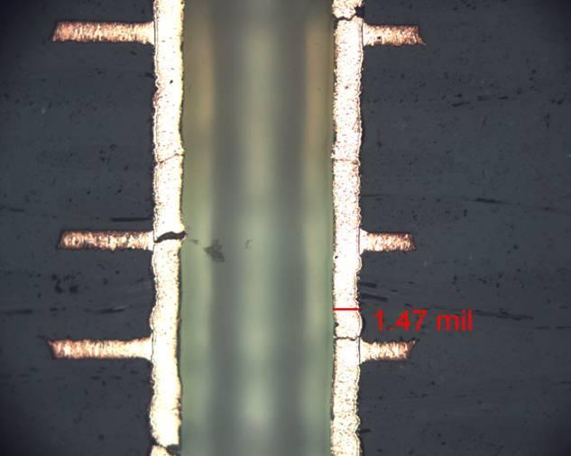
66 0.8mm pitch (above).100 pitch (right) FA ATC Example (G)

")


67 FA IST As Built Example (G)

")
68 FA for IST after 6X Reflow Some materials delaminated at 1.00 mm pitch also Eyebrow cracking also found Example of Eyebrow Cracking (D) Example of Delamination (I)
Interconnection Reliability of HDI Printed Wiring Boards
 Presented in the ECWC 10 Conference at IPC Printed Circuits Expo, SMEMA Council APEX and Designers Summit 05 Interconnection Reliability of HDI Printed Wiring Boards Tatsuo Suzuki Nec Toppan Circuit Solutions,
IBM Laminate Study Group
 IBM Laminate Study Group Lead-Free Laminate Robustness Brett Krull, Dept FM2 Nov 18, 2009 Agenda Introductions Laminate Robustness Background Qualification Methods Contributing Factors Past Work on Laminate
Via Life vs. Temperature Stress Analysis of Interconnect Stress Test
 Page 1 of 12 N P All BNP Media LINX Search H i 3 w Want to use this article? CLICK HERE for options!
ICDs (InterConnect Defects) What are they? Where do they come from? How can we make them go away? Doug Trobough Suixin Zhang
 What are they? Where do they come from? How can we make them go away? Doug Trobough Suixin Zhang") ICDs (InterConnect Defects) What are they? Where do they come from? How can we make them go away? Doug Trobough Suixin Zhang Definition of ICD ICDs are any defect that occurs adjacent to the innerlayer
ICDs (InterConnect Defects) What are they? Where do they come from? How can we make them go away? Doug Trobough Suixin Zhang Definition of ICD ICDs are any defect that occurs adjacent to the innerlayer
Pad Crater Project Definition Stage. Joe Smetana Alcatel-Lucent For Member Meeting 2/9/2011 San Jose, CA
 Pad Crater Project Definition Stage Joe Smetana Alcatel-Lucent For Member Meeting 2/9/2011 San Jose, CA The issue(s) Pad Cratering defects are a significant challenge with Pb-free PCB materials and/or
IMPACT OF MICROVIA-IN-PAD DESIGN ON VOID FORMATION
 IMPACT OF MICROVIA-IN-PAD DESIGN ON VOID FORMATION Frank Grano, Felix Bruno Huntsville, AL Dana Korf, Eamon O Keeffe San Jose, CA Cheryl Kelley Salem, NH Joint Paper by Sanmina-SCI Corporation EMS, GTS
Component Palladium Lead Finish - Specification Approved by Executive Board 1997-xx-xx August 22 Version
 Component Palladium Lead Finish - Specification Approved by Executive Board 1997-xx-xx August 22 Version Appendices 1. User Commitment Form 2. Supplier Compliance Form Table of contents 1. Background 2.
Lead Free Assembly: A Practical Tool For Laminate Materials Selection
 Lead Free Assembly: A Practical Tool For Laminate Materials Selection Erik J. Bergum David Humby Isola Abstract: The impending European RoHS legislation, restricting the use of lead containing solders,
14. Designing with FineLine BGA Packages
 14. Designing with FineLine BGA Packages S51014-1.0 Chapter 14, Designing with FineLine BGA Packages, replaces AN 114: Designing with FineLine BGA Packages. Introduction As programmable logic devices (PLDs)
Highly Accelerated Thermal Shock Reliability Testing
 Highly Accelerated Thermal Shock Reliability Testing by Bob E. Neves Microtek Laboratories, Inc. Anaheim CA and Rick B. Snyder Delphi Delco Electronics Systems, Inc. Kokomo IN and Timothy A. Estes Conductor
IPC-AJ-820A Assembly and Joining Handbook. The How and Why of All Things PCB & PCA
 IPC-AJ-820A Assembly and Joining Handbook The How and Why of All Things PCB & PCA 1 Scope To provide guidelines and supporting info for the mfg of electronic equipment To explain the HOW TO and WHY Discussions
IPC-TM-650 TEST METHODS MANUAL
 3000 Lakeside Drive, Suite 309S Bannockburn, IL 60015-1249 TEST METHODS MNUL Number Conductive nodic Filament (CF) Resistance Test: X-Y xis Originating Task Group Electrochemical Migration Task Group (5-32e)
INTERFLUX ELECTRONICS NV
 Reflow soldering temperature profiling Min : 30sec Max : 120sec Max : +4 C/sec Max : 250 C Min : 230 C Min: +0,5 C/sec Min : +1 C/sec Max : +3 C/sec Max : +1 C/sec Max : -6 C/sec Min : -2 C/sec Min : +1
Evaluating the CAF (conductive anodic filament)
") Technology report Evaluating the CAF (conductive anodic filament) resistance of multi-layered PWBs Akiko Kobayashi, Yuichi Aoki, Keiko To Headquarters ESPEC Corp. Technical Development A dvances in the
Technology report Evaluating the CAF (conductive anodic filament) resistance of multi-layered PWBs Akiko Kobayashi, Yuichi Aoki, Keiko To Headquarters ESPEC Corp. Technical Development A dvances in the
System Level Effects on Solder Joint Reliability
 System Level Effects on Solder Joint Reliability Maxim Serebreni 2004 2010 Outline Thermo-mechanical Fatigue of solder interconnects Shear and tensile effects on Solder Fatigue Effect of Glass Style on
Lead-Free HASL: Balancing Benefits and Risks for IBM Server and Storage Hardware
 Lead-Free HASL: Balancing Benefits and Risks for IBM Server and Storage Hardware November 19, 2009 M.Kelly, P.Eng, MBA Senior Engineer, ECAT Interconnect Technology Lead-Free Server Development Core Team
Freescale Semiconductor Tape Ball Grid Array (TBGA) Overview
 Overview") Freescale Semiconductor Tape Ball Grid Array (TBGA) Overview Revision 0 2006 Freescale and the Freescale logo are trademarks of Freescale Semiconductor, Inc. All other product or service names are the
Freescale Semiconductor Tape Ball Grid Array (TBGA) Overview Revision 0 2006 Freescale and the Freescale logo are trademarks of Freescale Semiconductor, Inc. All other product or service names are the
Characterizing the Lead-Free Impact on PCB Pad Craters
 Characterizing the Lead-Free Impact on PCB Pad Craters Brian Roggeman and Wayne Jones Advanced Process Lab Universal Instruments Corp. Binghamton, NY 13902 Abstract Pad cratering in Printed Circuit Boards
Low CTE / High Tg FR-4 with High Heat Resistance
 Low CTE / High Tg FR-4 with High Heat Resistance Laminate: EM-827 Prepreg: EM-827B 1 Features Tg(DSC) > 170 Z direction CTE < 3.0% (50~260 ) High thermal degradation temperature: Td > 340 Excellent thermal
Newsletter. Test Services & Failure Analysis Laboratory. April The Reality of Flip-Chip Solder Bump Electromigration Failure INSIDE THIS ISSUE
 Test Services & Failure Analysis Laboratory April 2008 Newsletter INSIDE THIS ISSUE Features Solder Bump Electromigration Failure Solder Joint Failure Criteria External Inspection of PCBs Hollow Fibers
BASE MATERIALS Through Assembly
 Thermal Analysis of BASE MATERIALS Through Assembly Can current analytical techniques predict and characterize differences in laminate performance prior to exposure to thermal excursions during assembly?
inemi BFR-Free Free PCB Material Evaluation Project Chair : Stephen Tisdale Intel Corporation SMTAi Presentation August 21, 2008
 inemi BFR-Free Free PCB Material Evaluation Project Chair : Stephen Tisdale Intel Corporation SMTAi Presentation August 21, 2008 0 Co-Authors Gary B. Long Intel Corporation Hillsboro, OR Gary.B.Long@Intel.com
TMS320C6000 BGA Manufacturing Considerations
 TMS320C6000 BGA Manufacturing Considerations David Bell C6000 Applications Team Abstract When designing with a high-density BGA package, it is important to be aware of different techniques that aid in
Welcome to the KEMET Ceramic Capacitor Flex Crack Mitigation product training module. This module will review sources of stress in surface mount
 1 Welcome to the KEMET Ceramic Capacitor Flex Crack Mitigation product training module. This module will review sources of stress in surface mount multilayer ceramic capacitors, provide board layout recommendations,
Pb-free Challenges for High Complexity Products. inemi Jan 16 th 2008
 Pb-free Challenges for High Complexity Products inemi Jan 16 th 2008 All Rights Reserved Alcatel-Lucent 2007 Agenda RoHS 101 Typical complex of telecom products (different from consumable) Pb-free Concerns
Offshore Wind Turbines Power Electronics Design and Reliability Research
 Offshore Wind Turbines Power Electronics Design and Reliability Research F. P. McCluskey CALCE/Dept. Of Mechanical Engineering University of Maryland, College Park, MD (301) 405-0279 mcclupa@umd.edu 1
Fairchild Semiconductor Application Note January 2001 Revised September Using BGA Packages
 Introduction AN-5026 Demanding space and weight requirements of personal computing and portable electronic equipment has led to many innovations in IC packaging. Combining the right interface and logic
Material Selection and Parameter Optimization for Reliable TMV Pop Assembly
 Selection and Parameter Optimization for Reliable TMV Pop Assembly Brian Roggeman, David Vicari Universal Instruments Corp. Binghamton, NY, USA Roggeman@uic.com Martin Anselm, Ph.D. - S09_02.doc Lee Smith,
Introduction Conductors. Supply Planes. Dielectric. Vias PCB Manufacturing Process Electronic Assembly Manufacturing Process
 PCBs/Overview Printed Circuit Boards (PCB) Introduction Conductors. Supply Planes. Dielectric. Vias PCB Manufacturing Process Electronic Assembly Manufacturing Process 29/09/2005 EE6471 (KR) 263 PCBs/Overview
How to select PCB materials for highfrequency
 How to select PCB materials for highfrequency apps Find out how to simplify that choice when striving for the best tradeoff between ease of fabrication and best electrical performance. By John Coonrod
EFFECT OF PRINTED WIRING BOARD WARPAGE ON BALL GRID ARRAYS OVER TEMPERATURE
 EFFECT OF PRINTED WIRING BOARD WARPAGE ON BALL GRID ARRAYS OVER TEMPERATURE Kyra Ewer and Jeffrey Seekatz Raytheon Dallas, TX ABSTRACT A study was undertaken to determine the extent to which a printed
Flexible PCB Plating Through Hole Considerations, Experiences and Solutions
 Presented in the ECWC 10 Conference at IPC Printed Circuits Expo, SMEMA Council APEX and Designers Summit 05 Flexible PCB Plating Through Hole Considerations, Experiences and Solutions Neil Patton Atotech
TECHNICAL DATA SHEET 1 P a g e Revised January 9, 2014
 1 P age Revised January 9, 2014 TAIYO PSR-4000 CC01SE (UL Name: PSR-4000JV / CA-40JV) LIQUID PHOTOIMAGEABLE CURTAIN COAT SOLDER MASK Curtain Coat Application Aqueous Developing Solder Mask RoHS Compliant
Validated Test Method to Characterize and Quantify Pad Cratering Under Bga Pads on Printed Circuit Boards
 Validated Test Method to Characterize and Quantify Pad Cratering Under Bga Pads on Printed Circuit Boards Mudasir Ahmad, Jennifer Burlingame, Cherif Guirguis Technology and Quality Group Cisco Systems,
PEC (Printed Electronic Circuit) process for LED interconnection
 process for LED interconnection") PEC (Printed Electronic Circuit) process for LED interconnection Higher wattage LED s/ power components or their placement in higher densities, requires a larger dissipation of heat in a more effective
PEC (Printed Electronic Circuit) process for LED interconnection Higher wattage LED s/ power components or their placement in higher densities, requires a larger dissipation of heat in a more effective
c/bach, 2-B Pol. Ind Foinvasa Montcada i Reixac (Barcelona) SPAIN Tel FAX
 SPAIN Tel FAX") 1- What is 2- How does it work? 3- How do we make it? 4- Applications 5- Processing? WHAT IS? Thick aluminium based substrate, cladded in ED copper foil. Designed for an effective thermal dissipation and
1- What is 2- How does it work? 3- How do we make it? 4- Applications 5- Processing? WHAT IS? Thick aluminium based substrate, cladded in ED copper foil. Designed for an effective thermal dissipation and
Effects of SAC Alloy Copper Dissolution Rates on PTH Processes: Cost and performance justify use of certain alternatives to SAC305/405
 Effects of SAC Alloy Copper Dissolution Rates on PTH Processes: Cost and performance justify use of certain alternatives to SAC305/405 1 Craig Hamilton, Polina Snugovsky (Celestica) & Matthew Kelly (IBM)
Optimizing the Insulated Metal Substrate Application with Proper Material Selection and Circuit Fabrication
 Abstract Optimizing the Insulated Metal Substrate Application with Proper Material Selection and Circuit Fabrication Dave Sommervold, Chris Parker, Steve Taylor, Garry Wexler. The Bergquist Company Prescott,
Simulation of Embedded Components in PCB Environment and Verification of Board Reliability
 Simulation of Embedded Components in PCB Environment and Verification of Board Reliability J. Stahr, M. Morianz AT&S Leoben, Austria M. Brizoux, A. Grivon, W. Maia Thales Global Services Meudon-la-Forêt,
EFFECT OF Ag COMPOSITION, DWELL TIME AND COOLING RATE ON THE RELIABILITY OF Sn-Ag-Cu SOLDER JOINTS. Mulugeta Abtew
 EFFECT OF Ag COMPOSITION, DWELL TIME AND COOLING RATE ON THE RELIABILITY OF Sn-Ag-Cu SOLDER JOINTS Mulugeta Abtew Typical PCB Assembly Process PCB Loading Solder Paste Application Solder Paste Inspection
High Frequency Circuit Materials Attributes John Coonrod, Rogers Corporation
 High Frequency Circuit Materials Attributes John Coonrod, Rogers Corporation Specialty high frequency circuit materials have been used in the PCB industry for decades and for many different reasons. There
GRAPHIC MANUFACTURING CAPABILITY Q217-18
 All features are design dependent and may not be achievable in combination Reduced Yield / Special values up ( or down ) to the standard limit are design and application dependent Standard features only
White Paper Quality and Reliability Challenges for Package on Package. By Craig Hillman and Randy Kong
 White Paper Quality and Reliability Challenges for Package on Package By Craig Hillman and Randy Kong Background Semiconductor technology advances have been fulfilling Moore s law for many decades. However,
Qualification and Performance Specification for Flexible Printed Boards
 Qualification and Performance Specification for Flexible Printed Boards Developed by the Flexible Circuits Performance Specifications Subcommittee (D-12) of the Flexible Circuits Committee (D-10) of IPC
ATS Document Cover Page
 221-008 Item Rev Status: RELEASED printed 9/20/2017 2:27:42 PM by Les Deenin ATS: OPERATIN PROCEDURE ATS Document Cover Page Responsible Department: Supply Chain This copy is uncontrolled unless otherwise
Flex and Rigid-Flex Printed Circuit Design
 Flex and Rigid-Flex Printed Circuit Design Old Content - visit altium.com/documentation Modified by on 29-Nov-2016 Related Videos Bending Lines Enhanced Layer Stack Management Layer Stack Regions A rigid-flex
Becoming Lead Free. Automotive Electronics. Antonio Aires Soldering Technical Specialist Visteon Corporation - Palmela Plant
 Automotive Electronics Becoming Lead Free Antonio Aires Soldering Technical Specialist Visteon Corporation - Palmela Plant 1 Agenda 1. Leadfree Electronics Drivers 2. Requirements 3. Areas of Impact 4.
PWB Creeping Corrosion Mechanism and Mitigation Strategy
 PWB Creeping Corrosion Mechanism and Mitigation Strategy Jim Kenny, Karl Wengenroth, Ted Antonellis, ShenLiang Sun, Dr. Cai Wang, Edward Kudrak, Dr. Joseph Abys Enthone Inc., Cookson Electronics West Haven,
Smart Integration of Thermal Management Systems for Electronics Cooling
 Smart Integration of Thermal Management Systems for Electronics Cooling Dr. Ir. Wessel W. Wits, University of Twente, Faculty of Engineering Technology, Laboratory of Design, Production and Management,
SOLDER JOINT RELIABILITY TEST SUMMARY
 Project Number: SJR Tracking Code: TC0623-SEAF-SJR-1059 Requested by: Jeremy Wooldridge Date: 05/20/2008 Product Rev: D (SEAF), C (SEAM) Part #: SEAF-50-5.0-S-10-2-A/ SEAM-50-2.0-S-10-2-A SEAF-50-6.5-S-10-1-A/
PCB Technologies for LED Applications Application note
 PCB Technologies for LED Applications Application note Abstract This application note provides a general survey of the various available Printed Circuit Board (PCB) technologies for use in LED applications.
PERFORMANCE SPECIFICATION
 METRI MIL-PRF-31032/3 22 June 1997 PERFORMANE SPEIFIATION PRINTED WIRING BOARD, FLEXIBLE, SINGLE AND DOUBLE LAYER, WITH OR WITHOUT PLATED HOLES, WITH OR WITHOUT STIFFENERS, FOR SOLDERED PART MOUNTING This
Lead-Free Connectors - An Overview
 Lead-Free Connectors - An Overview Pete Elmgren Molex Inc. 15 August 2003 Introduction For more than 50 years, lead-bearing solders have been used almost exclusively throughout the electronics industry
U.S. EPA-IPC Design for the Environment Printed Wiring Board Project Making Holes Conductive Performance Testing Results
 U.S. EPA-IPC Design for the Environment Printed Wiring Board Project Making Holes Conductive Performance Testing Results Introduction Methods and Materials Discussion Acknowledgments Appendices: 1. Test
contaminated, or if the location of the assembly house is well above sea level.
 VAPOR PHASE REFLOW S EFFECT ON SOLDER PASTE RESIDUE SURFACE INSULATION RESISTANCE Karen Tellefsen. Mitch Holtzer, Corne Hoppenbrouwers Alpha Assembly Solutions South Plainfield, NJ, USA Roald Gontrum SmartTech
ThunderClad 2. TU-883 HF Very Low Loss Material. Laminates & Prepregs Mass Lamination Service Insulated Metal Substrate Materials
 ThunderClad 2 TU-883 HF Very Low Loss Material Laminates & Prepregs Mass Lamination Service Insulated Metal Substrate Materials TUC Product Roadmap 2 ULVP VLP HCF Ultra Low Void Prepreg Very Low Profile
UL PCB Recognition what is it & why do you need to know about it
 UL PCB Recognition what is it & why do you need to know about it Presented by Emma Hudson NCAB Customer Event March 2015 UL and the UL logo are trademarks of UL LLC 2015 Agenda What is UL and what are
WorkShop Audace. INSA ROUEN 8 juin 2012
 WorkShop Audace INSA ROUEN 8 juin 2012 Global Standards for the Microelectronics Industry JEDEC standards for product level qualification Christian Gautier Content JEDEC overview Environmental reliability
Composition/wt% Bal SA2 (SABI) Bal SA3 (SABI + Cu) Bal
 Bal SA3 (SABI + Cu) Bal") Improving Thermal Cycle and Mechanical Drop Impact Resistance of a Lead-free Tin-Silver-Bismuth-Indium Solder Alloy with Minor Doping of Copper Additive Takehiro Wada 1, Seiji Tsuchiya 1, Shantanu Joshi
Improving Thermal Cycle and Mechanical Drop Impact Resistance of a Lead-free Tin-Silver-Bismuth-Indium Solder Alloy with Minor Doping of Copper Additive Takehiro Wada 1, Seiji Tsuchiya 1, Shantanu Joshi
PARTIALLY-ACTIVATED FLUX RESIDUE INFLUENCE ON SURFACE INSULATION RESISTANCE OF ELECTRONIC ASSEMBLY
 As originally published in the SMTA Proceedings. PARTIALLY-ACTIVATED FLUX RESIDUE INFLUENCE ON SURFACE INSULATION RESISTANCE OF ELECTRONIC ASSEMBLY Xiang Wei, Ph.D., Kyle Loomis, Jennifer Allen, Bruno
Via Filling: Challenges for the Chemistry in the Plating Process
 Via Filling: Challenges for the Chemistry in the Plating Process Mike Palazzola Nina Dambrowsky and Stephen Kenny Atotech Deutschland GmbH, Germany Abstract Copper filling of laser drilled blind micro
Thermo-Mechanical Reliability of Through-Silicon Vias (TSVs)
") 1 Thermo-Mechanical Reliability of Through-Silicon Vias (TSVs) Xi Liu Ph.D. Student and Suresh K. Sitaraman, Ph.D. Professor The George W. Woodruff School of Mechanical Engineering Georgia Institute of
1 Thermo-Mechanical Reliability of Through-Silicon Vias (TSVs) Xi Liu Ph.D. Student and Suresh K. Sitaraman, Ph.D. Professor The George W. Woodruff School of Mechanical Engineering Georgia Institute of
Quality and Reliability Report
 Quality and Reliability Report Product Qualification MAAM-008819 2mm 8-Lead PDFN Plastic Package QTR-0147 M/A-COM Technology Solutions Inc. 100 Chelmsford Street Lowell, MA 01851 Tel: (978) 656-2500 Fax:
Impact of Conductive Polymer Cathode Systems with Tantalum. Capacitors. Ta Ta
 Capacitor Seminar: Conductive Cathodes in ntalum and Aluminum SMD Capacitors For the past fifteen years, the tantalum capacitor has had enormous improvements in ESR because of the replacement of MnO 2
Acceptance Testing Of Low-Ag Reflow Solder Alloys
 Acceptance Testing Of Low-Ag Reflow Solder Alloys Kris Troxel 1, Aileen Allen 2, Elizabeth Elias Benedetto 3, Rahul Joshi 3 Hewlett-Packard Company 1 Boise, ID, USA 2 Palo Alto, CA, USA 3 Houston, TX,
IMPLEMENTATION OF A FULLY MOLDED FAN-OUT PACKAGING TECHNOLOGY
 IMPLEMENTATION OF A FULLY MOLDED FAN-OUT PACKAGING TECHNOLOGY B. Rogers, C. Scanlan, and T. Olson Deca Technologies, Inc. Tempe, AZ USA boyd.rogers@decatechnologies.com ABSTRACT Fan-Out Wafer-Level Packaging
Development of System in Package
 Development of System in Package In recent years, there has been a demand to offer increasingly enhanced performance for a SiP that implements downsized and lower-profile chips at lower cost. This article
Basic PCB Level Assembly Process Methodology for 3D Package-on-Package
 Basic PCB Level Assembly Process Methodology for 3D Package-on-Package Vern Solberg STC-Madison Madison, Wisconsin USA Abstract The motivation for developing higher density IC packaging continues to be
PCB Production Process HOW TO PRODUCE A PRINTED CIRCUIT BOARD
 NCAB Group Seminars PCB Production Process HOW TO PRODUCE A PRINTED CIRCUIT BOARD NCAB GROUP PCB Production Process Introduction to Multilayer PCBs 2 Introduction to multilayer PCB s What is a multilayer
Nano- And Micro-Filled Conducting Adhesives For Z-axis Interconnects
 Nano- And Micro-Filled Conducting Adhesives For Z-axis Interconnects We take a look at micro-filled epoxy-based conducting adhesives modified with nanoparticles for z- axis interconnections, especially
Improvement of Laser Fuse Processing of Fine Pitch Link Structures for Advanced Memory Designs
 Improvement of Laser Fuse Processing of Fine Pitch Link Structures for Advanced Memory Designs Joohan Lee, Joseph J. Griffiths, and James Cordingley GSI Group Inc. 60 Fordham Rd. Wilmington, MA 01887 jlee@gsig.com
Dallas Semicoductor DS80C320 Microcontroller
 Construction Analysis Dallas Semicoductor DS80C320 Microcontroller Report Number: SCA 9702-525 Global Semiconductor Industry the Serving Since 1964 15022 N. 75th Street Scottsdale, AZ 85260-2476 Phone:
METRIC The documentation and process conversion measures necessary to comply with this revision shall be completed by: 2 December 2017.
 METRIC The documentation and process conversion measures necessary to comply with this revision shall be completed by: 2 December 2017. MIL PRF 31032/2C 2 June 2017 SUPERSEDING MIL PRF 31032/2B w/amendment
Sample Preparation for Mitigating Tin Whiskers in alternative Lead-Free Alloys
 As originally published in the IPC APEX EXPO Conference Proceedings. Sample Preparation for Mitigating Tin Whiskers in alternative Lead-Free Alloys Mehran Maalekian Karl Seelig, V.P. Technology Timothy
Optical Connector Characteristics and Their Impact on System Performance and Reliability
 Optical Connector Characteristics and Their Impact on System Performance and Reliability There are a large number of issues that affect the performance of fiber optic connectors in today s networks. These
Conductive Anodic Filament Growth Failure
 Presented at IPC Printed Circuits Expo www.ipcprintedcircuitexpo.org Conductive Anodic Filament Growth Failure Tarun Amla Isola Abstract With increasing focus on reliability and miniaturized designs, Conductive
MATERIALS. September Construction Profiles and Material Decomposition p.18. Improved Thin-Film Resistor Material p.24
 September 2013 Construction Profiles and Material Decomposition p.18 MATERIALS Improved Thin-Film Resistor Material p.24 High-Frequency Laminates for Hybrid Multilayer PCBs p.30 Material Selection for
Power quad flat no-lead (PQFN) package
 package") NXP Semiconductors Application Note Document Number: AN2467 Rev. 5.0, 7/2016 Power quad flat no-lead (PQFN) package 1 Purpose This document provides guidelines for handling and assembly of NXP PQFN packages
NXP Semiconductors Application Note Document Number: AN2467 Rev. 5.0, 7/2016 Power quad flat no-lead (PQFN) package 1 Purpose This document provides guidelines for handling and assembly of NXP PQFN packages
The hand soldering process can therefore be defined by the following steps ;
 Hand Soldering with Lead Free Alloys Introduction As companies start to implement lead free soldering processes, hand soldering and associated techniques have been identified as key functions in the manufacturing
Failure Modes in Wire bonded and Flip Chip Packages
 Failure Modes in Wire bonded and Flip Chip Packages Mumtaz Y. Bora Peregrine Semiconductor San Diego, Ca. 92121 mbora@psemi.com Abstract The growth of portable and wireless products is driving the miniaturization
EPOXY FLUX MATERIAL AND PROCESS FOR ENHANCING ELECTRICAL INTERCONNECTIONS
 As originally published in the SMTA Proceedings. EPOXY FLUX MATERIAL AND PROCESS FOR ENHANCING ELECTRICAL INTERCONNECTIONS Neil Poole, Ph.D., Elvira Vasquez, and Brian J. Toleno, Ph.D. Henkel Electronic
The Packaging and Reliability Qualification of MEMS Resonator Devices
 The Packaging and Reliability Qualification of MEMS Resonator Devices Pavan Gupta Vice President, Operations Yin-Chen Lu, Preston Galle Quartz and MEMS Oscillators source: www.ecliptek.com Quartz Oscillators:
HBLED packaging is becoming one of the new, high
 Ag plating in HBLED packaging improves reflectivity and lowers costs JONATHAN HARRIS, President, CMC Laboratories, Inc., Tempe, AZ Various types of Ag plating technology along with the advantages and limitations
Chips Face-up Panelization Approach For Fan-out Packaging
 Chips Face-up Panelization Approach For Fan-out Packaging Oct. 15, 2015 B. Rogers, D. Sanchez, C. Bishop, C. Sandstrom, C. Scanlan, TOlson T. REV A Background on FOWLP Fan-Out Wafer Level Packaging o Chips
BOARD LEVEL ASSEMBLY AND RELIABILITY CONSIDERATIONS FOR QFN TYPE PACKAGES
 BOARD LEVEL ASSEMBLY AND RELIABILITY CONSIDERATIONS FOR QFN TYPE PACKAGES Ahmer Syed and WonJoon Kang Amkor Technology, Inc. 1900 S. Price Road Chandler, Arizona ABSTRACT There is a strong interest in
Choosing the Correct Capillary Design for Fine Pitch, BGA Bonding
 Choosing the Correct Capillary Design for Fine Pitch, BGA Bonding Lee Levine, Principal Engineer phone 215-784-6036, fax 215-784-6402, email: llevine@kns.com and Michael J. Sheaffer, Director Technical
Thermosonic Gold Ball Bonding to Immersion Gold/Electroless Nickel Plating Finishes on Laminate MCM Substrates. Abstract.
 Thermosonic Gold Ball Bonding to Immersion Gold/Electroless Nickel Plating Finishes on Laminate MCM Substrates Chris Dunn, R. Wayne Johnson Mike Bozack Auburn University 200 Broun Hall, EE Dept. Auburn,
EXTREME LONG TERM PRINTED CIRCUIT BOARD SURFACE FINISH SOLDERABILITY ASSESSMENT
 EXTREME LONG TERM PRINTED CIRCUIT BOARD SURFACE FINISH SOLDERABILITY ASSESSMENT Gerard O Brien, Solderability Testing and Solutions Inc., Richmond, KY Dave Hillman, Rockwell Collins, Cedar Rapids, IA INTRODUCTION
Lead-Free Solder Bump Technologies for Flip-Chip Packaging Applications
 Lead-Free Solder Bump Technologies for Flip-Chip Packaging Applications Zaheed S. Karim 1 and Jim Martin 2 1 Advanced Interconnect Technology Ltd. 1901 Sunley Centre, 9 Wing Yin Street, Tsuen Wan, Hong
TGV and Integrated Electronics
 TGV and Integrated Electronics Shin Takahashi ASAHI GLASS CO., LTD. 1 Ambient Intelligence Green Energy/Environment Smart Factory Smart Mobility Smart Mobile Devices Bio/Medical Security/Biometrics 2 Glass
HKPCA Journal Issue 21
 Conductive Anodic Filament: Mechanisms and Affecting Factors Winco K.C. Yung, PhD, Associate Professor PCB Technology Centre, Department of Industrial and Systems Engineering, The Hong Kong Polytechnic
PERFORMANCE SPECIFICATION PRINTED WIRING BOARD, RIGID GENERAL SPECIFICATION FOR
 The document and process conversion measures necessary to comply with this revision shall be completed by 31 December 1997. INCH-POUND MIL-PRF-55110F 31 May 1997 SUPERSEDING MIL-PRF-55110E 31 December
THIN IMMERSION TIN USING ORGANIC METALS
 THIN IMMERSION TIN USING ORGANIC METALS Jim Kenny, Nils Arendt, Bernhard Wessling, and Karl Wengenroth Enthone Inc., A Business of Cookson Electronics West Haven, CT, USA ABSTRACT With the international
PARYLENE ENGINEERING. For Longer Lasting Products
 PARYLENE ENGINEERING For Longer Lasting Products PARYLENE ENGINEERING This presentation serves as a quick overview of the conformal coating material and processes currently used in the industry. The field
The Effect of Reflow Profiling on the Electrical Reliability of No-Clean Solder Paste Flux Residues
 The Effect of Reflow Profiling on the Electrical Reliability of No-Clean Solder Paste Flux Residues Authored by: Eric Bastow, Indium Corporation Abstract An estimated 80% of all SMT assembly in the world