Probing Challenges with Cu Pillar. Phill Mai, JEM America Joe Mai, JEM Europe
|
|
|
- Ella Hines
- 5 years ago
- Views:
Transcription


1 Probing Challenges with Cu Pillar Phill, JEM America Joe, JEM Europe
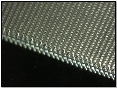
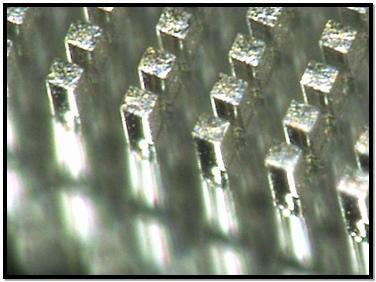
2 Crown-tip probe limitations MEMS probe with flat tip Summary Future work Overview 2


3 Crown-to-bump contact Piercing Contact Probe mark Abrasive/Gel Cleaning 3
4 Crown-to-bump CRES stability Cleaning Cycle_TT Sheet CRES vs TDS 抵抗値 (Ω) Cleaning Frequency 200 TDs Test conditions: Crown tip dia: φ65 μm Bump: Pb-free, φ90 x 65 μm Probing OD: 50 μm from last pin Cleaning OD: 100 μm from avg. pin height Frequency: every 200 TDs Number of TDs/clean: 10 Lateral movement: X390 μm, Y390 μm after each TD CRES of probe only; test cabling subtracted TD 数 Touchdowns 4


5 Crown-to-Cu pillar contact Slicing Contact Probe mark Abrasive/Gel Cleaning not so effective in the long term 5
 HT")


6 Initial Crown-to-Cu pillar CRES stability Current: 50mA RT (30 ) HT (125 ) LT (-35 ) 200TD CL10TD 200TD CL10TD 200TD CL10TD *CRES includes about 2 ohms of resistance due to PCB, Space transformer, Interposer, and probe body. 6


7 Long term Crown-to-Cu pillar CRES stability Adhesion of SnAg causes CRES instability after 50K TDs 7


8 Crown Tip Contamination with eutectic solder Before laser After laser Pb debris remains In 2007 Laser: IMT800MV Beam dia.: ~3 mm 8


9 Crown Tip Contamination with Pb-free solder REF: Probe Card Cleaning by Laser, J.M. Lee et.al., SWTW 2010 Si peak is from cleaning sheet. Before laser In 2016 Laser: IMT400P Beam dia.: ~3 mm After laser Only probe materials Only probe materials 9

10 MEMS Technology (MT) as an Alternative 10
11 MT Probe Card Structure PCB Stiffener Interposer (Reflow) Space transformer Upper guide plate &Upper stiffener plate MEMS Probe Bottom guide plate &Bottom stiffener plate 11
 structure optimizes mechanical and electrical")

12 MT Probe characteristics Straight probe allows easy assembly and maintenance Composite (multi-layer) structure optimizes mechanical and electrical properties, and reduces probe wear. Tip material: Pd alloy MT Probe Upper guide plate Bottom guide plate 50μm 55μm Before lateral slide After lateral slide 12


13 MT PROBE MECHANICS Initial OD160μm Limit OD recommended OD (from last touch) 13


14 Guide Plate Selection Bending Strength Guide plate A Hardened surface [MPa] A B C D E Silicon Guide Plate Si SiO2 A-484 (Al2O3) SN-240 (Si3N4) Guide plate materials Hardened surface Guide plate A has high bending strength and low friction. 14


15 Probe : 2.5g Contact force version Probe Force Hysteresis Initial Guide Plate Optimized Guide Plate Top Probe force hysteresis Difference Sample Difference int 1M N1 0.65gf 2.28gf N2 0.57gf 1.72gf Difference Difference Sample Difference int 1M N1 0.13gf 0.44gf N2 0.18gf 0.56gf Bottom Ave. 0.61gf 2.00gf Ave. 0.16gf 0.50gf 15


16 Guide-plate Wear View: Top of the Guide Plate Oblique Angle View Top Initial Guide Plate Wear :4.4~5.5μm(n=5) Optimized Guide Plate Bottom Wear :2.1~3.1μm(n=4) 16

17 MT-to-Cu Pillar Probe Mark (multiple contacts) RT Temp TD counts 1st 2nd 5th 1st 2nd 5th 1st 2nd 5th Contact Mark Percentage of flatto-initial diameter 34% 36% 38% 49% 54% 60% 27% 28% 30% Contact Mark Diameter (μm) Contact Mark Depression (μm)

 HT (125 ) LT (-35 ) 200TD")

18 Current: 50 ma OD: 70μm (from last pin) Cleaning Sheet: WA6000 lapping paper Cleaning Sheet OD: 70μm (from last pin) Flat-to-Cu pillar CRES Stability RT (30 ) HT (125 ) LT (-35 ) 200TD CL3TD *CRes includes ~2 ohms of resistance due to PCB, Space transformer, Interposer, and probe body. 18
")
19 Current-Carrying Capacity (CCC) 19
20 Maximum Allowable Current (MAC) MT probe for 80 um pitch Contact OD:MT 70μm / VS 100μm 1 min-on/1 sec- off Current: 600, 650, 700, 750mA Number of Pins: 3 pins for MT and VS MAC : ~650mA 20
21 Sparameter Model G S_P S_N G Bandwidth MT80 - Differential S11 MT80 - Differential S21 Pitch:80μm Length:7.23mm < -20dB up to 10GHz -1dB at 20 GHz 21
22 Summary Probing Cu pillars with minimal bump damage and stable CRES is challenging. Crown tips can be used, but tip cleaning is difficult and requires offline laser cleaning. Flat-tip MT probes are effective for probing 35 µm dia. Cu pillars if low-friction guide plates and low probe forces are used. MT probes have high CCC and MAC even with small probe crosssections. 22

23 Future Work Develop 40um pitch MT probe. Increase CCC of 60-um-pitch probe to at least 500 ma. Develop pointed tips for Al pad contact. Optimize overdrive vs. temperature to minimize bump damage Increase max. temperature to 175 C. ST side Wafer side 23
24 Atsushi Mine, JEM Japan ITS Acknowledgements 24
Fine Pitch P4 Probe Cards
 Fine Pitch P4 Probe Cards Photolithographic Pattern Plating Process June 1998 By Toshi Ishii, Hide Yoshida Contents What is a P4 probe card? Specification Some test results Tip cleaning RF performance
28nm Mobile SoC Copper Pillar Probing Study. Jose Horas (Intel Mobile Communications) Amy Leong (MicroProbe) Darko Hulic (Nikad)
 Amy Leong (MicroProbe) Darko Hulic (Nikad)") 28nm Mobile SoC Copper Pillar Probing Study Jose Horas (Intel Mobile Communications) Amy Leong (MicroProbe) Darko Hulic (Nikad) Overview Introduction to IMC Copper Pillar Implementation at IMC Low force
28nm Mobile SoC Copper Pillar Probing Study Jose Horas (Intel Mobile Communications) Amy Leong (MicroProbe) Darko Hulic (Nikad) Overview Introduction to IMC Copper Pillar Implementation at IMC Low force
Global Test solutions Conception and production of probe cards for testing microchips
 Global Test solutions Conception and production of probe cards for testing microchips All Technologies Synergie Cad Probe developed differents solution of test, it is became a leader in the design and
Experience in Applying Finite Element Analysis for Advanced Probe Card Design and Study. Krzysztof Dabrowiecki Jörg Behr
 Experience in Applying Finite Element Analysis for Advanced Probe Card Design and Study Krzysztof Dabrowiecki Jörg Behr Overview A little bit of history in applying finite element analysis for probe card
Study on microprobe processing by LIGA on Si
 Study on microprobe processing by LIGA on Si Fundamental study for 3-D 3 D mold -Report 1-1 Teppei Kimura, JEM Japan (Japan Electronic Materials Corp.) Tadashi Hattori Himeji Institute of Technology in
Probing Lead Free Solder Bumps in Final Wafer Test
 Probing Lead Free Solder Bumps in Final Wafer Test By Sam McKnight Southwest Test Workshop June 2002 Microelectronics Outline Why lead free? Background Info Focus areas Setup Lead/Tin and Tin Rich results
High Performance Spring Probe and 0.35mm pitch Elastomeric Contact by Stamping Process
 High Performance Spring Probe and 0.35mm pitch Elastomeric Contact by Stamping Process Company Logo Samuel Pak, A.J. Park IWIN Co. Ltd. 363-883 South Korea, Choongbuk, Chungwon, Ohchang- eup Yangchung-
Flip Chip Applications
 June 12 to 15, 2011 San Diego, CA WSP Wafer Wafer Socket Probe for Flip Chip Applications Brandon Mair bmair@ti.com Norman Armendariz norm@ti.com TTC Test Technology Center Agenda Introduction Probe Tip
Conductive Paste-Based Interconnection Technology for High Performance Probe Card
 Conductive Paste-Based Interconnection Technology for High Performance Probe Card Sang-il Kwon Eddy Kang TSE Co., Ltd. Overview Introduction of TABP Technology Key Technology of Core to Core Interconnection
March 15-18, 2015 Hilton Phoenix / Mesa Hotel Mesa, Arizona Archive Session 4
 Proceedings March 15-18, 2015 Hilton Phoenix / Mesa Hotel Mesa, Arizona Archive Session 4 2015 BiTS Workshop Image: BCFC/iStock Session 4 Rafiq Hussain Session Chair BiTS Workshop 2015 Schedule Performance
Fritting Experiences with non-ohmic contact resistance C RES while wafer test probing
 Fritting Experiences with non-ohmic contact resistance C RES while wafer test probing Jan Martens Philips Semiconductors Hamburg Awarded Best Overall Presentation at SWTW-2006 Overview Fritting What s
Online Semi-radius Probe Tip Cleaning and Reshaping
 Online Semi-radius Probe Tip Cleaning and Reshaping Authors: Sam McKnight and Michael Agbesi IEEE SW Test Workshop 1 Agenda Acknowledgements Background info Setup and measurement technique Contact resistance
Transverse Load Analysis For Semiconductor Applications
 Transverse Load Analysis For Semiconductor Applications Presenters: Soheil Khavandi Co-authors: Parker Fellows Robert Hartley Jordan James Aaron Lomas Advisor: Jerry Broz, Ph.D. UNR Owen Stedham Award
Flip Chip Bump Electromigration Reliability: A comparison of Cu Pillar, High Pb, SnAg, and SnPb Bump Structures
 Flip Chip Bump Electromigration Reliability: A comparison of Cu Pillar,,, and SnPb Bump Structures Ahmer Syed, Karthikeyan Dhandapani, Lou Nicholls, Robert Moody, CJ Berry, and Robert Darveaux Amkor Technology
Investigating Copper Metallurgy Effects for Sort Process and Cleaning Performance Metrics
 Jan Martens NXP Semiconductors Germany Simon Allgaier Feinmetall GmbH Jerry Broz, Ph.D. International Test Solutions Investigating Copper Metallurgy Effects for Sort Process and Cleaning Performance Metrics
Novel Methodologies for Assessing On-line Probe Process Parameters
 Novel Methodologies for Assessing On-line Probe Process Parameters Jerry J. Broz, Ph.D. Brice Blanc Gene Humphrey International Test Solutions 5690 Riggins Court Reno, Nevada 89502 Rhett Moore Micron Technology,
Evaluation of Cu Pillar Chemistries
 Presented at 2016 IMAPS Device Packaging Evaluation of Cu Pillar Chemistries imaps Device Packaging Conference Spring 2016 Matthew Thorseth, Mark Scalisi, Inho Lee, Sang-Min Park, Yil-Hak Lee, Jonathan
Wafer probe challenges for the automotive market Luc Van Cauwenberghe
 Wafer probe challenges for the automotive market Luc Van Cauwenberghe ON Semiconductor Overview Automotive wafer probe requirements Results of experiments Summary Follow on Work Acknowledgements 2 Automotive
Methodologies for Assessing On-line Probe Process Parameters
 Jan Martens NXP Semiconductors Germany Simon Allgaier Feinmetall GmbH Jerry Broz, Ph.D. International Test Solutions Methodologies for Assessing On-line Probe Process Parameters June 8-11, 8 2008 San Diego,
Aluminum Probe Pad Thickness and Properties for Stable Parametric Probe Ability
 Aluminum Probe Pad Thickness and Properties for Stable Parametric Probe Ability Presenter: Bernd Bischoff (TI Germany) Co authors: Jerry Broz (ITS) Swen Harder (FFI) Uwe Schiessl (TI Germany) Seyedsoheil
A Real Life Pad Crack Study
 A Real Life Pad Crack Study Gunther Boehm (FM) Jory Twitchell (NXP) Matthias Schnaithmann (FM) Overview What are pad cracks? Challenge and objective Initial Experiment first qualification run Main experiment
Interlayer Dielectric (ILD) Cracking Mechanisms and their Effects on Probe Processes. Daniel Stillman, Daniel Fresquez Texas Instruments Inc.
 Cracking Mechanisms and their Effects on Probe Processes. Daniel Stillman, Daniel Fresquez Texas Instruments Inc.") Interlayer Dielectric (ILD) Cracking Mechanisms and their Effects on Probe Processes Daniel Stillman, Daniel Fresquez Texas Instruments Inc. Outline Probe Optimization Why is it needed? Objective and obstacles
Interlayer Dielectric (ILD) Cracking Mechanisms and their Effects on Probe Processes Daniel Stillman, Daniel Fresquez Texas Instruments Inc. Outline Probe Optimization Why is it needed? Objective and obstacles
Anisotropic Conductive Films (ACFs)
") Anisotropic Conductive Films (ACFs) ACF = Thermosetting epoxy resin film + Conductive particles Chip or substrate 1 Heat Pressure ACF Substrate 2 Chip or substrate 1 ACF Substrate 2 Applications Chip-on-Board
Anisotropic Conductive Films (ACFs) ACF = Thermosetting epoxy resin film + Conductive particles Chip or substrate 1 Heat Pressure ACF Substrate 2 Chip or substrate 1 ACF Substrate 2 Applications Chip-on-Board
Ultralow Residue Semiconductor Grade Fluxes for Copper Pillar Flip-Chip
 Ultralow Residue Semiconductor Grade Fluxes for Copper Pillar Flip-Chip SzePei Lim (Presenter), Jason Chou, Maria Durham, and Dr. Andy Mackie Indium Corporation 1 Outline of Presentation Roadmaps and challenges
Case studies of Wafer Sort Floor Problems. Darren James SWTW Committee Member
 Case studies of Wafer Sort Floor Problems Darren James SWTW Committee Member Applying What We Learned We ve completed Gage R&R Study We know we have a solid metrology tool We know the limits of our metrology
Cu Pillar Interconnect and Chip-Package-Interaction (CPI) for Advanced Cu Low K chip
 for Advanced Cu Low K chip") EPRC 12 Project Proposal Cu Pillar Interconnect and Chip-Package-Interaction (CPI) for Advanced Cu Low K chip 15 th Aug 2012 Page 1 Introduction: Motivation / Challenge Silicon device with ultra low k
EPRC 12 Project Proposal Cu Pillar Interconnect and Chip-Package-Interaction (CPI) for Advanced Cu Low K chip 15 th Aug 2012 Page 1 Introduction: Motivation / Challenge Silicon device with ultra low k
curamik CERAMIC SUBSTRATES AMB technology Design Rules Version #04 (09/2015)
") curamik CERAMIC SUBSTRATES AMB technology Design Rules Version #04 (09/2015) Content 1. Geometric properties 1.01. Available ceramic types / thicknesses... 03 1.02. thicknesses (standard)... 03 3. Quality
curamik CERAMIC SUBSTRATES AMB technology Design Rules Version #04 (09/2015) Content 1. Geometric properties 1.01. Available ceramic types / thicknesses... 03 1.02. thicknesses (standard)... 03 3. Quality
Material based challenge and study of 2.1, 2.5 and 3D integration
 1 Material based challenge and study of 2.1, 2.5 and 3D integration Toshihisa Nonaka Packaging Solution Center R&D Headquarters Hitachi Chemical Co., Ltd., Sep. 8, 2016 Hitachi Chemical Co., Ltd. 2010.
Lead Free Soldering Technology
 Lead Free Soldering Technology Chung-Ang University Young-Eui Shin Trend of Package Small, Light, High performance High speed, Large capacity High integrity, High density Comparison of package size 45mm
Advanced Analytical Techniques for Semiconductor Assembly Materials and Processes. Jason Chou and Sze Pei Lim Indium Corporation
 Advanced Analytical Techniques for Semiconductor Assembly Materials and Processes Jason Chou and Sze Pei Lim Indium Corporation Agenda Company introduction Semiconductor assembly roadmap challenges Fine
Characterization of Coined Solder Bumps on PCB Pads
 Characterization of Coined Solder Bumps on PCB Pads Jae-Woong Nah, Kyung W. Paik, Won-Hoe Kim*, and Ki-Rok Hur** Department of Materials Sci. & Eng., Korea Advanced Institute of Science and Technology
New method to measure CCC (Current Carrying Capability) of thin probe wire
 of thin probe wire") New method to measure CCC (Current Carrying Capability) of thin probe wire Probe Innovation USA President Tadashi Rokkaku 1. Outline 1.1. General Definition of CCC : Current in wire at definite temperature
New method to measure CCC (Current Carrying Capability) of thin probe wire Probe Innovation USA President Tadashi Rokkaku 1. Outline 1.1. General Definition of CCC : Current in wire at definite temperature
Sn623-5T-E SOLDER PASTE
 Sn623-5T-E SOLDER PASTE INTRODUCTION Singapore Asahi s solder paste Sn623-5T-E is a silver bearing paste to prevent silver migration and brittleness. It is formulated for fine pitch applications up to
TECHNICAL DATA SHEET 1 / 7 MATERIALS BERYLLIUM COPPER BERYLLIUM COPPER BERYLLIUM COPPER POLYETHER ETHERCETONE 30% GF
 .. pn ao TECHNICAL DATA SHEET 1 / 7 All dimensions are in mm. COMPONENTS BODY CENTER CONTACT OUTER CONTACT INSULATOR GASKET OTHERS PARTS MATERIALS BERYLLIUM COPPER BERYLLIUM COPPER BERYLLIUM COPPER POLYETHER
S3X58-M ICT Compatible Lead Free Solder Paste. Product Information. Koki no-clean LEAD FREE solder paste. Contents.
 Koki no-clean LEAD FREE solder paste www.ko-ki.co.jp #53002 Revised on Mar. 3, 2015 ICT Compatible Lead Free Solder Paste Product Information Conventional Product Picture of ICT Checker Probe The product
Low Temperature Curable Positive Tone Photosensitive Polyimide Photoneece LT series. Toray Industries, Inc.
 Low Temperature Curable Positive Tone Photosensitive Polyimide Photoneece LT series Toray Industries, Inc. 1 The features of LT series (1) Low temperature curable ( ~170 ) Less damage for weak semiconductor
How Bad's the Damage?
 How Bad's the Damage? Evaluating Probe Damage On Aluminum, Solder, Gold, UBM, and Copper Pads. Ken Smith Vice President of Technology Development Pyramid Probe Division, Cascade Microtech Goal of Presentation
Pyramid Probe Card: P800-S Online Cleaning
 Pyramid Probe Card: P800-S Online Cleaning Quick Reference Guide Objective Particulate contamination can build up on the probe face and tips during probing. In some cases, particulate contamination may
Session 5. Burn-in & Test Socket Workshop Mechanical Aspects
 Session 5 Burn-in & Test Socket Workshop 2000 Mechanical Aspects BURN-IN & TEST SOCKET WORKSHOP COPYRIGHT NOTICE The papers in this publication comprise the proceedings of the 2000 BiTS Workshop. They
Challenges for Embedded Device Technologies for Package Level Integration
 Challenges for Embedded Device Technologies for Package Level Integration Kevin Cannon, Steve Riches Tribus-D Ltd Guangbin Dou, Andrew Holmes Imperial College London Embedded Die Technology IMAPS-UK/NMI
An Advanced Probe Characterization Tool Outline
 An Advanced Probe Characterization Tool An Advanced Probe Characterization Tool for Online Contact Basics Measurements p June, 7th 2005, San Diego (CA) Oliv (Infineon Technologies AG, Munich, Germany)
Whisker Generation Mechanism of Lead-free Soldered Joints
 Whisker Generation Mechanism of Lead-free Soldered Joints Mutsumi YOSHINO Masaki SANJI Syuntaro IGURO Due to the environmental restriction of SOC (Substances of Concern) in Europe, the lead-free solder
TOP VIEW SIDE VIEW. Description: Clam shell socket for 4.5x12.5mm, 0.4mm pitch QFN74 SECTION B-B SECTION A-A. CG-QFN-7010 Drawing.
 3.00 THRU ALL A A1 corner GHz QFN Socket - Direct mount, solderless Features A 25.48 Directly mounts to target PCB (needs tooling holes) with hardware High speed, reliable Elastomer connection Minimum
Electrical and Fluidic Microbumps and Interconnects for 3D-IC and Silicon Interposer
 Electrical and Fluidic Microbumps and Interconnects for 3D-IC and Silicon Interposer Li Zheng, Student Member, IEEE, and Muhannad S. Bakir, Senior Member, IEEE Georgia Institute of Technology Atlanta,
WF6317. A superactive low-volatile/high heat-resistant water-soluble flux for ball soldering
 WF637 A superactive low-volatile/high heat-resistant water-soluble flux for ball soldering Low viscosity and high tacking power stabilize ball holding force and ensures excellent solder wettability Easy
Cover. Wiper. Base. Shaft
 TURNS INTERNAL STRUCTURE!! FEATURES Lead-free soldering, Cadmium-free Fine adjustment is possible Automatic mounting is possible (Taping) Flow/reflow soldering is possible Sealed construction (Washable)
TGV and Integrated Electronics
 TGV and Integrated Electronics Shin Takahashi ASAHI GLASS CO., LTD. 1 Ambient Intelligence Green Energy/Environment Smart Factory Smart Mobility Smart Mobile Devices Bio/Medical Security/Biometrics 2 Glass
P 2 / 6 3.Dimensions 1.6± Quantity (Standard Quantity) 0.8± ~ ~ ±0.15 Products quantity in a reel 4,000 pcs./1 reel 1.The
 0.8± ~ ~ ±0.15 Products quantity in a reel 4,000 pcs./1 reel 1.The") Chip NTC Thermistor for temperature sensor and temperature compensation 0603 size P 1 / 6 1.Part Numbering. (ex.) NC U 18 XH 103 F 60 RB Product ID Series Dimensions Temperature Resistance Resistance Individual
Chip NTC Thermistor for temperature sensor and temperature compensation 0603 size P 1 / 6 1.Part Numbering. (ex.) NC U 18 XH 103 F 60 RB Product ID Series Dimensions Temperature Resistance Resistance Individual
M705-GRN360 K-Series
 Senju Metal Industry Co.,Ltd. High-Reliability Lead-Free Solder Paste M705-GRN360 K-Series Manufacturer Senju Metal Industry Co.,Ltd. 23 Senju Hashido-cho, Adachi-Ku, Tokyo, Japan Phone: +81-33888-5156
Freescale Semiconductor Tape Ball Grid Array (TBGA) Overview
 Overview") Freescale Semiconductor Tape Ball Grid Array (TBGA) Overview Revision 0 2006 Freescale and the Freescale logo are trademarks of Freescale Semiconductor, Inc. All other product or service names are the
Freescale Semiconductor Tape Ball Grid Array (TBGA) Overview Revision 0 2006 Freescale and the Freescale logo are trademarks of Freescale Semiconductor, Inc. All other product or service names are the
Design For Probe: Probe Card Selection Process
 Design For Probe: Probe Card Selection Process Brandon Mair Dawn Copeland 6/10/2014 Agenda DFP Overview TI Qualified Vendors Qualification Process Probe Technologies Specifications / Documentation Benefits
Lead-Free Solder Bump Technologies for Flip-Chip Packaging Applications
 Lead-Free Solder Bump Technologies for Flip-Chip Packaging Applications Zaheed S. Karim 1 and Jim Martin 2 1 Advanced Interconnect Technology Ltd. 1901 Sunley Centre, 9 Wing Yin Street, Tsuen Wan, Hong
Probe Card Cleaning Media Survey. Eric Hill, Josh Smith : : June 10, 2008
 Probe Card Cleaning Media Survey Eric Hill, Josh Smith : : Special Thanks To: IEEE SW Test Workshop 2 Outline Introduction Materials and Methods Results Conclusions Acknowledgments IEEE SW Test Workshop
In-line Hybrid Metrology Solutions
 In-line Hybrid Metrology Solutions Brad Lawrence Regional Sales & Product Marketing Manager, XwinSys ED-XRF Based Metrology with Hybrid Sensor Technology Hybrid Sensor In-Line Metrology Process feedback
Hi-performance S3X58-M406
 www.ko-ki.co.jp Ver. 42004.5 Prepared on Mar. 7, 2005 Koki no-clean LEAD FREE solder paste Hi-performance Product information 0.4mm pitch 0.3mm diameter This Product Information contains product performance
High-reliability Low-Ag Alloy
 http://www.ko-ki.co.jp #47002E 2009.8.18 Koki no-clean LEAD FREE solder paste High-reliability Low-Ag Alloy PAT. pend Product information Sn0.3Ag0.7Cu S01X7C- alloy After -40+125ºC 1500cycle This Product
3DIC Integration with TSV Current Progress and Future Outlook
 3DIC Integration with TSV Current Progress and Future Outlook Shan Gao, Dim-Lee Kwong Institute of Microelectronics, A*STAR (Agency for Science, Technology and Research) Singapore 9 September, 2010 1 Overview
PRODUCT SPECIFICATION FOR APPROVAL
 Issue : 151XC14C08005 Date of Issue : October 27.2008 DIGI-KEY CORPORATION : New Changed PRODUCT SPECIFICATION FOR APPROVAL Product Description Product Part Number : Common Mode Noise Filter (RoHS) : EXC14CE900U
MEPTEC Semiconductor Packaging Technology Symposium
 MEPTEC Semiconductor Packaging Technology Symposium Advanced Packaging s Interconnect Technology Process Shift and Direction October 23, 2014 Jay Hayes- Director of Business Development -Bumping and Flip
New probe tip fabricated by MEMS (LIGA process) for no-cleaning test
 for no-cleaning test") New probe tip fabricated by MEMS (LIGA process) for no-cleaning test Tsuyoshi Haga, K.Okada, J.Yorita, Y.Hirata, S.Shimada* Harima R&D Department Osaka R&D Laboratories *Analysis Technology Research Center
New probe tip fabricated by MEMS (LIGA process) for no-cleaning test Tsuyoshi Haga, K.Okada, J.Yorita, Y.Hirata, S.Shimada* Harima R&D Department Osaka R&D Laboratories *Analysis Technology Research Center
A Flexible Vertical MEMs Probe Card Technology for Pre-Bump and ewlp Applications
 June 12 to 15, 2011 San Diego, CA A Flexible Vertical MEMs Probe Card Technology for Pre-Bump and ewlp Applications Mike Slessor Rick Marshall (MicroProbe, Inc.) Vertical MEMS for Pre-Bump Probe Introduction:
Ultra Fine Pitch Bumping Using e-ni/au and Sn Lift-Off Processes
 Ultra Fine Pitch Bumping Using e-ni/au and Sn Lift-Off Processes Andrew Strandjord, Thorsten Teutsch, and Jing Li Pac Tech USA Packaging Technologies, Inc. Santa Clara, CA USA 95050 Thomas Oppert, and
Modified Tool for Developmental Analysis and Real Time QRA Probe Card and Socket Results
 Modified Tool for Developmental Analysis and Real Time QRA Probe Card and Socket Results Terence Q. Collier CVInc Richardson, Texas TQCollier@covinc.com Collier, TQ 1 The "Old Way" Test Analysis Limitations
Micro burn-in techniques at wafer-level test to implement cost effective solutions
 Micro burn-in techniques at wafer-level test to implement cost effective solutions Geert Gouwy Arnaud Devos Alessandro Antonioli Raffaele Vallauri Agenda 1. Melexis Company Overview 2. Automotive Safety
LPSC SiCap 100µm NiAu finishing - Assembly by soldering
 General description This document describes the attachment techniques recommended by Murata* for their LPSC silicon capacitors on the customer substrates. This document is non-exhaustive. Customers with
An Innovative High Throughput Thermal Compression Bonding Process
 An Innovative High Throughput Thermal Compression Bonding Process Li Ming 2 September 2015 Outline Introduction Throughput improved TCB Process Liquid Phase Contact (LPC) bonding Flux-LPC-TCB under inert
3D-WLCSP Package Technology: Processing and Reliability Characterization
 3D-WLCSP Package Technology: Processing and Reliability Characterization, Paul N. Houston, Brian Lewis, Fei Xie, Ph.D., Zhaozhi Li, Ph.D.* ENGENT Inc. * Auburn University ENGENT, Inc. 2012 1 Outline Packaging
Evaluation of Cantilever Probe-Induced Dielectric Cracks in Cu/Low-k Devices
 Evaluation of Cantilever Probe-Induced Dielectric Cracks in Cu/Low-k Devices C.D. Hartfield, D. Stillman, J. Aronoff Texas Instruments, Dallas, TX SouthWest Test Workshop - 2004 Outline Objectives Background
Chip NTC Thermistor for temperature sensor and temperature compensation 0805 size
 P 1 / 6 Chip NTC Thermistor for temperature sensor and temperature compensation 0805 size 1. Part Numbering (ex.) NC P 21 XV 103 J 03 RA Product ID Series Dimensions Temperature Resistance Resistance Individual
SMD RFI CLIP Data Sheet
 1/14 Attn : Data Sheet - CONDITION : 1. 2. 3. 4. We approved the product as above. WRITE REVIEW APPROVAL ICT NAME S.P. HONG J.E. KIM S.K,JUNG SIGNATURE Supplier : Innochips Technology CO., LTD By President
R Series : IMP SMT BOARD TO BOARD ADAPTATOR H3 REEL OF 600 TECHNICAL DATA SHEET 1 / 7 COMPONENTS MATERIALS.
 .. pn ao TECHNICAL DATA SHEET 1 / 7 All dimensions are in mm. COMPONENTS BODY CENTER CONTACT OUTER CONTACT INSULATOR GASKET OTHERS PARTS MATERIALS BERYLLIUM COPPER BERYLLIUM COPPER BERYLLIUM COPPER POLYETHER
Innovative Substrate Technologies in the Era of IoTs
 Innovative Substrate Technologies in the Era of IoTs Dyi- Chung Hu 胡迪群 September 4, 2015 Unimicron Contents Introduction Substrate Technology - Evolution Substrate Technology - Revolution Glass substrate
Low Melting Point Lead Free Solder Paste
 www.ko-ki.co.jp #49005E Revised on Nov 17, 2011 Koki no-clean LEAD FREE solder paste Koki no-clean LEAD FREE solder paste Low Melting Point Lead Free Solder Paste TB48-M742 & Product information This Product
XBSC/UBDC/UBSC/BBSC/ULSC 100 µm & 400 µm - Assembly by soldering
 Assembly by soldering General description This document describes the attachment techniques recommended by Murata* for their pre-bumped and un-bumped silicon capacitors on the customer substrates. This
Electrical and Mechanical Characterization of BladeRunner Tips on Reflowed Eutectic Bumps
 Electrical and Mechanical Characterization of BladeRunner Tips on Reflowed Eutectic Bumps Dr. Rod Martens Sr. Principal Engineer FormFactor, Inc. Scott Mitchell Program Manager Strategic Probe Development
TSV Processing and Wafer Stacking. Kathy Cook and Maggie Zoberbier, 3D Business Development
 TSV Processing and Wafer Stacking Kathy Cook and Maggie Zoberbier, 3D Business Development Outline Why 3D Integration? TSV Process Variations Lithography Process Results Stacking Technology Wafer Bonding
DITF ToolKit 1. Standard Substrate Sizes (selected at the factory for optimum process)
") DITF ToolKit 1 DITF Toolkit Substrates Common Substrate Materials Alumina (99.5% min) єr = 9.9 Tan d = 1.5 x10⁻⁴ Aluminum Nitride (K170) єr = 8.9 Tan d = 2.0 x10⁻³ Beryllia (99.5%) єr = 6.7 Tan d = 3.0
DITF ToolKit 1 DITF Toolkit Substrates Common Substrate Materials Alumina (99.5% min) єr = 9.9 Tan d = 1.5 x10⁻⁴ Aluminum Nitride (K170) єr = 8.9 Tan d = 2.0 x10⁻³ Beryllia (99.5%) єr = 6.7 Tan d = 3.0
Packaging Effect on Reliability for Cu/Low k Damascene Structures*
 Packaging Effect on Reliability for Cu/Low k Damascene Structures* Guotao Wang and Paul S. Ho Laboratory of Interconnect & Packaging, TX 78712 * Work supported by SRC through the CAIST Program TRC 2003
PRODUCT SPECIFICATION FL3215T-000X. Digi-Key Corporation
 TDK Corporation Corporate Headquarters 13-1,Nihonbashi 1-chome,Chuo-ku Tokyo 103-8272 Japan Phone : Tokyo(03)5201-7229 PRODUCT SPECIFICATION Branch Office Sales div. Phone ( ) SPEC.No. C479NAA00005_1 DATE
LGIT CSP Application NOTE. (Lighting)
") LGIT CSP Application NOTE (Lighting) TABLE OF CONTENTS 1. LGIT CSP Detail -------------- P2 2. LGIT CSP PCB Design -------------- P3 2.1. LGIT CSP Footprint and PCB Pattern -------------- P3 2.2. PCB Substrate
LGIT CSP Application NOTE (Lighting) TABLE OF CONTENTS 1. LGIT CSP Detail -------------- P2 2. LGIT CSP PCB Design -------------- P3 2.1. LGIT CSP Footprint and PCB Pattern -------------- P3 2.2. PCB Substrate
ASPICS IPD Companion for ISM Transceiver IC: RF front end part
 IPD Companion for ISM Transceiver IC: RF front end part Rev 1.2 TD Introduction The ASPICS320.606 is an integrated passives device specifically designed for use with the SEMTECH SX1211 868/915MHz ISM/UHF
NARROW PITCH (0.4mm) CONNECTORS P4S SERIES
 CONNECTORS P4S SERIES") FOR BOARD-TO-BOARD AND BOARD-TO-FPC CONNECTION AXT3, 4 NARROW PITCH (0.4mm) CONNECTORS P4S SERIES NEW 2. Strong resistance to adverse environments! Utilizes construction for high contact reliability. 1)
FOR BOARD-TO-BOARD AND BOARD-TO-FPC CONNECTION AXT3, 4 NARROW PITCH (0.4mm) CONNECTORS P4S SERIES NEW 2. Strong resistance to adverse environments! Utilizes construction for high contact reliability. 1)
ALPHA OM-5100 FINE PITCH SOLDER PASTE
 SM 797-7 ALPHA OM-5100 FINE PITCH SOLDER PASTE DESCRIPTION Cookson Electronics Assembly Material s ALPHA OM-5100, is a low residue, no-clean solder paste designed to maximize SMT line yields. The flux
Murata Silicon Capacitors - LPSC 100µm NiAu finishing Assembly by Soldering. Table of Contents
 Table of Contents Table of Contents...1 Introduction...2 Handling precautions and storage...2 Pad opening...3 Process Flow...5 Solder print material and stencil printing recommendations...6 Pick and Place...7
THE EFFECTS OF INTERNAL STRESSRS IN BGA Ni LAYER ON THE STRENGTH OF Sn/Ag/Cu SOLDER JOINT
 THE EFFECTS OF INTERNAL STRESSRS IN BGA Ni LAYER ON THE STRENGTH OF Sn/Ag/Cu SOLDER JOINT C.H. Chien 1, * C.J. Tseng 1,2 T.P. Chen 1,3 1 Department of Mechanical and Electro-Mechanical Engineering, National
NARROW PITCH (0.4mm) CONNECTORS P4S SERIES
 CONNECTORS P4S SERIES") FOR BOARD-TO-BOARD AND BOARD-TO-FPC CONNECTION NARROW PITCH (0.4mm) CONNECTORS P4S SERIES Compliance with RoHS Directive http://www.mew.co.jp/ac/e/ FEATURES 1. Space saving Compared to the currently sold
FOR BOARD-TO-BOARD AND BOARD-TO-FPC CONNECTION NARROW PITCH (0.4mm) CONNECTORS P4S SERIES Compliance with RoHS Directive http://www.mew.co.jp/ac/e/ FEATURES 1. Space saving Compared to the currently sold
CHALLENGING NEW TECHNOLOGIES
 T4AB58-M742 Koki no-clean LEAD FREE solder paste www.ko-ki.co.jp #49005-1 Revised on Sep. 30, 2014 Koki no-clean LEAD FREE solder paste Low Melting Point Lead Free Solder Paste T4AB58-M742 Product information
HTSC SiCap 400µm - NiAu finishing - Assembly by soldering
 General description This document describes the attachment techniques recommended by Murata* for their HTSC silicon capacitors on the customer substrates. This document is non-exhaustive. Customers with
MECHANICAL PROPERTIES OF Sn3.5Ag AND Sn3.8Ag0.7Cu SOLDER BALLS FOR BGA PACKAGE
 221 MECHANICAL PROPERTIES OF AND Sn3.8Ag0.7Cu SOLDER BALLS FOR BGA PACKAGE A. Jalar 1, B.Y. Majlis 2, I.Ahmad 2 and E.P. Leng 3 1 School of Applied Physics, University Kebangsaan Malaysia, Selangor, Malaysia
Electromigration in Flip Chip Solder Joints
 Electromigration in Flip Chip Solder Joints K.N. Tu Dept. of Materials Science & Engineering, UCLA 1. Introduction 2. Why does electromigration in solder joint become a reliability problem? 3. Electromigration
Kingbright. L-36BID T-1 (3mm) Blinking LED Lamp DESCRIPTIONS PACKAGE DIMENSIONS FEATURES APPLICATIONS ATTENTION SELECTION GUIDE
 Blinking LED Lamp DESCRIPTIONS PACKAGE DIMENSIONS FEATURES APPLICATIONS ATTENTION SELECTION GUIDE") T-1 (3mm) Blinking LED Lamp DESCRIPTIONS The High Efficiency Red source color devices are made with Gallium Arsenide Phosphide on Gallium Phosphide Orange Light Emitting Diode Electrostatic discharge and
T-1 (3mm) Blinking LED Lamp DESCRIPTIONS The High Efficiency Red source color devices are made with Gallium Arsenide Phosphide on Gallium Phosphide Orange Light Emitting Diode Electrostatic discharge and
Chips Face-up Panelization Approach For Fan-out Packaging
 Chips Face-up Panelization Approach For Fan-out Packaging Oct. 15, 2015 B. Rogers, D. Sanchez, C. Bishop, C. Sandstrom, C. Scanlan, TOlson T. REV A Background on FOWLP Fan-Out Wafer Level Packaging o Chips
High-Reliability Lead-Free Solder Paste M705-GRN360-K-V. Senju Metal Industry Co.,Ltd. Senju Manufacturing (Europe) Ltd.
 Ltd.") Senju Metal Industry Co., Ltd. High-Reliability Lead-Free Solder Paste Manufacturer Senju Metal Industry Co.,Ltd. 23 Senju Hashido-cho, Adachi-Ku, Tokyo, Japan Phone: +81-33888-5156 Fax: +81-33870-3032
Senju Metal Industry Co., Ltd. High-Reliability Lead-Free Solder Paste Manufacturer Senju Metal Industry Co.,Ltd. 23 Senju Hashido-cho, Adachi-Ku, Tokyo, Japan Phone: +81-33888-5156 Fax: +81-33870-3032
3D-IC Integration using D2C or D2W Alignment Schemes together with Local Oxide Reduction
 3D-IC Integration using D2C or D2W Alignment Schemes together with Local Oxide Reduction Gilbert Lecarpentier*, Jean-Stéphane Mottet* SET S.A.S. (Smart Equipment Technology), 131 Impasse Barteudet, 74490
Developments in low-temperature metal-based packaging
 Developments in low-temperature metal-based packaging 2011. 12.14 Jiyoung Chang and Liwei Lin Ph.D. Candidate, Department of Mechanical Engineering University of California at Berkeley 1 1 Contents Project
operating current (*1) (*5) NCU18XH103F60RB 10k±1% 3380±1% Reference Only Thermal Dissipation Constant (mw/ C) (*1)
 (*5) NCU18XH103F60RB 10k±1% 3380±1% Reference Only Thermal Dissipation Constant (mw/ C) (*1)") Chip NTC Thermistor for temperature sensor and temperature compensation 0603 size P / 8.Part Numbering. (ex.) NC U 8 XH 03 F 60 RB Product ID Series Dimensions Temperature Resistance Resistance Individual
Chip NTC Thermistor for temperature sensor and temperature compensation 0603 size P / 8.Part Numbering. (ex.) NC U 8 XH 03 F 60 RB Product ID Series Dimensions Temperature Resistance Resistance Individual
Challenges and Solutions for Cost Effective Next Generation Advanced Packaging. H.P. Wirtz, Ph.D. MiNaPAD Conference, Grenoble April 2012
 Challenges and Solutions for Cost Effective Next Generation Advanced Packaging H.P. Wirtz, Ph.D. MiNaPAD Conference, Grenoble April 2012 Outline Next Generation Package Requirements ewlb (Fan-Out Wafer
Kingbright. L-56BID T-1 3/4 (5mm) Blinking LED Lamp DESCRIPTIONS PACKAGE DIMENSIONS FEATURES APPLICATIONS ATTENTION SELECTION GUIDE
 Blinking LED Lamp DESCRIPTIONS PACKAGE DIMENSIONS FEATURES APPLICATIONS ATTENTION SELECTION GUIDE") T-1 3/4 (5mm) Blinking LED Lamp DESCRIPTIONS The High Efficiency Red source color devices are made with Gallium Arsenide Phosphide on Gallium Phosphide Orange Light Emitting Diode Electrostatic discharge
T-1 3/4 (5mm) Blinking LED Lamp DESCRIPTIONS The High Efficiency Red source color devices are made with Gallium Arsenide Phosphide on Gallium Phosphide Orange Light Emitting Diode Electrostatic discharge
Reliability of RoHS-Compliant 2D and 3D 1С Interconnects
 Reliability of RoHS-Compliant 2D and 3D 1С Interconnects John H. Lau, Ph.D. New York Chicago San Francisco Lisbon London Madrid Mexico City Milan New Delhi San Juan Seoul Singapore Sydney Toronto Foreword