Cristaux 3D. Fabriquer de tels objets aux longueur d'ondes optiques???
|
|
|
- Lesley Tate
- 5 years ago
- Views:
Transcription


1 Cristaux 3D Fabriquer de tels objets aux longueur d'ondes optiques???


![lattice 6-layer [001] silica](/docs-images/81/84030447/images/2-2.jpg "diamond lattice F.")
2 A la main, une sphère l'une après l'autre... 5μm 5μm dissolve latex spheres 4-layer [111] silica diamond lattice 6-layer [001] silica diamond lattice F. Garcia-Santamaria et al., Adv. Mater. 14 (16), 1144 (2002)
3 Moins désespéré : C Up to ~ 27% gap for Si/air diamond-like: rods ~ bonds rod layer B A hole layer S. G. Johnson et al., Appl. Phys. Lett. 77, 3490 (2000)
4 Making Rods & Holes Simultaneously side view substrate Si top view
5 Making Rods & Holes Simultaneously expose/etch holes substrate A A A A A A A A A
6 Making Rods & Holes Simultaneously backfill with silica (SiO 2 ) & polish substrate A A A A A A A A A
7 Making Rods & Holes Simultaneously deposit another Si layer layer 1 substrate A A A A A A A A A
8 Making Rods & Holes Simultaneously dig more holes offset & overlapping layer 1 B B B B substrate B B B B B B B A A A B B B B B B B A A A B B B B B B B A A A
9 Making Rods & Holes Simultaneously backfill layer 1 B B B B substrate B B B B B B B A A A B B B B B B B A A A B B B B B B B A A A
10 Making Rods & Holes Simultaneously etc... and dissolve silica when done layer 1 layer 2 substrate layer 3 C C C C B B B B one period C B C B C B C B C A B C A B C A B C C B C B C B C B C A B C A B C A B C C A B C A B C A B C A B C B C B C B C A A A
11 Making Rods & Holes Simultaneously etc... hole layers layer 1 layer 2 substrate layer 3 C C C C B B B B one perio d C B C B C B C B C A B C A B C A B C C B C B C B C B C A B C A B C A B C C A B C A B C A B C A B C B C B C B C A A A
12 Making Rods & Holes Simultaneously etc... rod layers layer 1 layer 2 substrate layer 3 C C C C B B B B one perio d C B C B C B C B C A B C A B C A B C C B C B C B C B C A B C A B C A B C C A B C A B C A B C A B C B C B C B C A A A

13 M. Qi, H. Smith, MIT A More Realistic Schematic
14 e-beam Fabrication: Top View 5 μm M. Qi, H. Smith, MIT


15 M. Qi, H. Smith, MIT e-beam Fabrication: Side Views
16 Adding Defect Microcavities 740nm 450nm C C C C B' B B layer 3 B B 2 layer 1 layer n m layer 7 6 substrate Easiest defect: don t etch some B holes non-periodically distributed: suppresses sub-band structure low Q = easier to detect from planewave M. Qi, H. Smith, MIT
17 Structure tas de bois (Woodpile structure) Up to ~ 17% gap for Si/air diamond-like bonds K. Ho et al., Solid State Comm. 89, 413 (1994) H. S. Sözüer et al., J. Mod. Opt. 41, 231 (1994)

18 1.25 Periods of Woodpile (4 log layers = 1 period) Si gap S. Y. Lin et al., Nature 394, 251 (1998)


19 1.25 Periods of 1.55μm (4 log layers = 1 period) Si gap 180nm 1.3μm S. Y. Lin et al., Nature 394, 251 (1998)
20 Woodpile by Wafer Fusion 2nd substrate + logs, rotated 90 and flipped substrate + first log layer S. Noda et al., Science 289, 604 (2000)
21 Woodpile by Wafer Fusion fuse wafers together substrate + first log layer S. Noda et al., Science 289, 604 (2000)
22 Woodpile by Wafer Fusion dissolve upper substrate substrate + first log layer S. Noda et al., Science 289, 604 (2000)
23 Woodpile by Wafer Fusion double, double, toil and trouble S. Noda et al., Science 289, 604 (2000)
")
24 S. Noda et al., Science 289, 604 (2000) Woodpile by Wafer Fusion
25 S. Noda et al., Science 289, 604 (2000) Woodpile Gap from μm
")
26 S. Noda et al., Science 289, 604 (2000) Finally, a Defect!

27 Stacking by Micromanipulation microsphere into hole break off suspended layer lift up and move to substrate tap down holes onto spheres spheres enforce alignment goto a; K. Aoki et al., Appl. Phys. Lett. 81 (17), 3122 (2002)

28 Stacking by Micromanipulation K. Aoki et al., Appl. Phys. Lett. 81 (17), 3122 (2002)


29 Yes, it works: Gap at ~4μm 20 layers 50nm accuracy: (gap effects are limited by finite lateral size) K. Aoki et al., Nature Materials 2 (2), 117 (2003) 1μm
30 A Metal Photonic Crystal Start with Si woodpile in SiO 2 dissolve Si with KOH fill with Tungsten via chemical vapor deposition (CVD) (on thin TiN layer) dissolve SiO 2 with HF J. G. Fleming et al., Nature 417, 52 (2002)
31 Holographic Lithography Four beams make 3d-periodic interference pattern absorptive material (1.4μm) k-vector differences give reciprocal lattice vectors (i.e. periodicity) D. N. Sharp et al., Opt. Quant. Elec. 34, 3 (2002) & M. Campbell, Nature, 404, 53 (2000)
 give unit cell")
 & M.")
32 Holographic Lithography beam polarizations + amplitudes (8 parameters) give unit cell D. N. Sharp et al., Opt. Quant. Elec. 34, 3 (2002) & M. Campbell, Nature, 404, 53 (2000)
 & M.")
33 Holographic Lithography 10μm huge volumes, long-range periodic, fcc lattice backfill for high contrast D. N. Sharp et al., Opt. Quant. Elec. 34, 3 (2002) & M. Campbell, Nature, 404, 53 (2000)
![Holographic Lithography [111] cleavages simulated structure 5μm [111] closeup 1μm titania inverse](/docs-images/81/84030447/images/34-0.jpg "structure D. N. Sharp et al., Opt. Quant. Elec. 34, 3 (2002) & M.")
34 Holographic Lithography [111] cleavages simulated structure 5μm [111] closeup 1μm titania inverse structure D. N. Sharp et al., Opt. Quant. Elec. 34, 3 (2002) & M. Campbell, Nature, 404, 53 (2000)
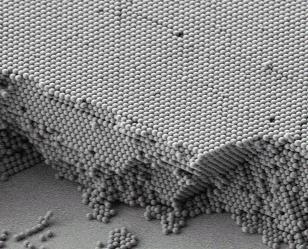
35 Colloids (opals) (evaporate) silica (SiO 2 ) microspheres (diameter < 1μm) sediment by gravity into close-packed fcc lattice!

36 Colloids (opals)
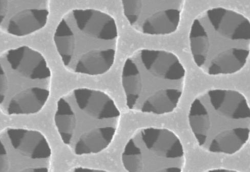
 complete band gap Remove Template Inverted Opal ~ 10% gap between 8th & 9th bands small gap, upper bands: sensitive to")
37 Inverse opals fcc solid spheres do not have a gap but fcc spherical holes in Si do have a gap 3D sub-micron colloidal spheres Infiltration Template (synthetic opal) complete band gap Remove Template Inverted Opal ~ 10% gap between 8th & 9th bands small gap, upper bands: sensitive to disorder
 & Colvin et al., Chem. Mater.")
38 A More Perfect Crystal meniscus 65 C 1 micron silica spheres in ethanol evaporate solvent 80 C Convective Assembly Heat Source Capillary forces during drying cause assembly in the meniscus Extremely flat, large-area opals of controllable thickness Nagayama, Velev, et al., Nature (1993) & Colvin et al., Chem. Mater. (1999)

39 A More Perfect Crystal

40 Inverse-Opal Photonic Crystal Y. A. Vlasov et al., Nature 414, 289 (2001)
41 Inverse-Opal Band Gap good agreement between theory (black) & experiment (red/blue) Y. A. Vlasov et al., Nature 414, 289 (2001)


 Wonmok,")
42 Inserting Defects in Inverse Opals e.g., Waveguides Three-photon lithography with laser scanning confocal microscope (LSCM) Wonmok, Adv. Materials 14, 271 (2002)


43 GLAD = GLancing Angle Deposition 15% gap for Si/air diamond-like with broken bonds doubled unit cell, so gap between 4th & 5th bands O. Toader and S. John, Science 292, 1133 (2001)
44 GLAD = GLancing Angle Deposition seed posts glancing-angle Si only builds up on protrusions evaporated Si rotate to spiral Si S. R. Kennedy et al., Nano Letters 2, 59 (2002)

45 GLAD = GLancing Angle Deposition S. R. Kennedy et al., Nano Letters 2, 59 (2002)
 S. Fan et al., Appl. Phys. Lett. 65, 1466 (1994) S. Kawakami et al., Appl. Phys. Lett. 74, 463 (1999)")
46 Auto-cloning start with an old layer-by-layer modify layering slightly (14% gap for Si/SiO 2 /air) (don t forget the holes) S. Fan et al., Appl. Phys. Lett. 65, 1466 (1994) S. Kawakami et al., Appl. Phys. Lett. 74, 463 (1999)
 bias sputtering cuts corners (prefers")

47 Competition between 3 processes clones shape of substrate Auto-cloning neutral atoms ions diffuse deposition leaves trenches (shadows) bias sputtering cuts corners (prefers 60 ) re-deposition fills trenches so, only planar patterning is in substrate only drilling needs alignment minimize etch roughness S. Kawakami et al., Appl. Phys. Lett. 74, 463 (1999)


48 Auto-cloning E. Kuramochi et al., Opt. Quantum. Elec. 34, 53 (2002)

 E. Yablonovitch, T. M. Gmitter, and K. M. Leung, Phys. Rev.")
49 Yablonovite diamond-like fcc crystal earliest fabrication-amenable alternative to diamond spheres image: (Topology is very similar to 2000 layer-by-layer crystal) E. Yablonovitch, T. M. Gmitter, and K. M. Leung, Phys. Rev. Lett. 67, 2295 (1991)

50 Making Yablonovite e-beam mask + chemically-assisted ion-beam etching GaAs 460nm C. C. Cheng et al., Physica Scripta. T68, 17 (1996)
 S i =3.1μm A. Chelnokov et al., Appl. Phys. Lett.")
51 Making ~Yablonovite (II) electrochemical + focused-ion-beam (FIB) etching (deep vertical holes) S i =3.1μm A. Chelnokov et al., Appl. Phys. Lett. 77, 2943 (2000)
Metodi di fabbricazione PhC
 Metodi di fabbricazione PhC PhC in 1D a n 1 n 2 z Deposizione multilayer (MBE,MOCVD,PVD,CVD) Silicio poroso Litografia Crescita per deposizione Physical deposition Chemical deposition InP by MOCVD Deposizione
Properties of Inverse Opal Photonic Crystals Grown By Atomic Layer Deposition
 Properties of Inverse Opal Photonic Crystals Grown By Atomic Layer Deposition J.S. King 1, C. W. Neff 1, W. Park 2, D. Morton 3, E. Forsythe 3, S. Blomquist 3, and C. J. Summers 1 (1) School of Materials
Supplementary Information
 Supplementary Information for Embedded Cavities and Waveguides in 3D Silicon Photonic Crystals by S. A. Rinne, F. García-Santamaría, and P. V. Braun, Nature Photonics, 2007 Figure S1. Figure S1 Detailed
ZnS-based photonic crystal phosphors fabricated using atomic layer deposition
 phys. stat. sol. (b) 241, No. 3, 763 766 (2004) / DOI 10.1002/pssb.200304287 ZnS-based photonic crystal phosphors fabricated using atomic layer deposition J. S. King *, 1, C. W. Neff 1, S. Blomquist 2,
Fabrication of photonic band-gap crystals
 Fabrication of photonic band-gap crystals C. C. Cheng and A. Scherer California Institute of Technology, Pasadena, California 91125 Received 19 June 1995; accepted 9 August 1995 We describe the fabrication
A discussion of crystal growth, lithography, etching, doping, and device structures is presented in
 Chapter 5 PROCESSING OF DEVICES A discussion of crystal growth, lithography, etching, doping, and device structures is presented in the following overview gures. SEMICONDUCTOR DEVICE PROCESSING: AN OVERVIEW
Microelectronics. Integrated circuits. Introduction to the IC technology M.Rencz 11 September, Expected decrease in line width
 Microelectronics Introduction to the IC technology M.Rencz 11 September, 2002 9/16/02 1/37 Integrated circuits Development is controlled by the roadmaps. Self-fulfilling predictions for the tendencies
Fabrication Process. Crystal Growth Doping Deposition Patterning Lithography Oxidation Ion Implementation CONCORDIA VLSI DESIGN LAB
 Fabrication Process Crystal Growth Doping Deposition Patterning Lithography Oxidation Ion Implementation 1 Fabrication- CMOS Process Starting Material Preparation 1. Produce Metallurgical Grade Silicon
Lect. 2: Basics of Si Technology
 Unit processes Thin Film Deposition Etching Ion Implantation Photolithography Chemical Mechanical Polishing 1. Thin Film Deposition Layer of materials ranging from fractions of nanometer to several micro-meters
Microstructural Characterization of Materials
 Microstructural Characterization of Materials 2nd Edition DAVID BRANDON AND WAYNE D. KAPLAN Technion, Israel Institute of Technology, Israel John Wiley & Sons, Ltd Contents Preface to the Second Edition
Low-cost, deterministic quasi-periodic photonic structures for light trapping in thin film silicon solar cells
 Low-cost, deterministic quasi-periodic photonic structures for light trapping in thin film silicon solar cells The MIT Faculty has made this article openly available. Please share how this access benefits
Review of CMOS Processing Technology
 - Scaling and Integration Moore s Law Unit processes Thin Film Deposition Etching Ion Implantation Photolithography Chemical Mechanical Polishing 1. Thin Film Deposition Layer of materials ranging from
Simple fabrication of highly ordered AAO nanotubes
 Journal of Optoelectronic and Biomedical Materials Volume 1, Issue 1, March 2009, p. 79-84 Simple fabrication of highly ordered AAO nanotubes N. Taşaltin a, S. Öztürk a, H. Yüzer b, Z. Z. Öztürk a,b* a
Czochralski Crystal Growth
 Czochralski Crystal Growth Crystal Pulling Crystal Ingots Shaping and Polishing 300 mm wafer 1 2 Advantage of larger diameter wafers Wafer area larger Chip area larger 3 4 Large-Diameter Wafer Handling
Assembly of Highly Ordered Three-Dimensional Porous Structure with Nanocrystalline TiO 2 Semiconductors
 Chem. Mater. 2002, 14, 83-88 83 Assembly of Highly Ordered Three-Dimensional Porous Structure with Nanocrystalline TiO 2 Semiconductors Q.-B. Meng,*,, C.-H. Fu, Y. Einaga, Z.-Z. Gu, A. Fujishima,, and
FABRICATION OF CMOS INTEGRATED CIRCUITS. Dr. Mohammed M. Farag
 FABRICATION OF CMOS INTEGRATED CIRCUITS Dr. Mohammed M. Farag Outline Overview of CMOS Fabrication Processes The CMOS Fabrication Process Flow Design Rules EE 432 VLSI Modeling and Design 2 CMOS Fabrication
CMOS Fabrication. Dr. Bassam Jamil. Adopted from slides of the textbook
 CMOS Fabrication Dr. Bassam Jamil Adopted from slides of the textbook CMOS Fabrication CMOS transistors are fabricated on silicon wafer Lithography process similar to printing press On each step, different
CSCI 4974 / 6974 Hardware Reverse Engineering. Lecture 5: Fabrication processes
 CSCI 4974 / 6974 Hardware Reverse Engineering Lecture 5: Fabrication processes QUIZ 3: CMOS layout Quiz Discussion Rationale If you know how something is put together, you can figure out how to take it
The Physical Structure (NMOS)
") The Physical Structure (NMOS) Al SiO2 Field Oxide Gate oxide S n+ Polysilicon Gate Al SiO2 SiO2 D n+ L channel P Substrate Field Oxide contact Metal (S) n+ (G) L W n+ (D) Poly 1 3D Perspective 2 3 Fabrication
The Physical Structure (NMOS) Al SiO2 Field Oxide Gate oxide S n+ Polysilicon Gate Al SiO2 SiO2 D n+ L channel P Substrate Field Oxide contact Metal (S) n+ (G) L W n+ (D) Poly 1 3D Perspective 2 3 Fabrication
Introduction to CMOS VLSI Design. Layout, Fabrication, and Elementary Logic Design
 Introduction to CMOS VLSI Design Layout, Fabrication, and Elementary Logic Design CMOS Fabrication CMOS transistors are fabricated on silicon wafer Lithography process similar to printing press On each
Polymer-based optical interconnects using nano-imprint lithography
 Polymer-based optical interconnects using nano-imprint lithography Arjen Boersma,Sjoukje Wiegersma Bert Jan Offrein, Jeroen Duis, Jos Delis, Markus Ortsiefer, Geert van Steenberge, MikkoKarppinen, Alfons
Microstructure of Electronic Materials. Amorphous materials. Single-Crystal Material. Professor N Cheung, U.C. Berkeley
 Microstructure of Electronic Materials Amorphous materials Single-Crystal Material 1 The Si Atom The Si Crystal diamond structure High-performance semiconductor devices require defect-free crystals 2 Crystallographic
Introduction to Lithography
 Introduction to Lithography G. D. Hutcheson, et al., Scientific American, 290, 76 (2004). Moore s Law Intel Co-Founder Gordon E. Moore Cramming More Components Onto Integrated Circuits Author: Gordon E.
Fabrication and Characterization of Two-Dimensional Photonic. Crystal Microcavities in Nanocrystalline Diamond
 Fabrication and Characterization of Two-Dimensional Photonic Crystal C. F. Wang, a),b) R. Hanson, a) D. D. Awschalom, a)c) E. L. Hu c),d) University of California, Santa Barbara, California 93106 T. Feygelson,
Fabrication and Layout
 ECEN454 Digital Integrated Circuit Design Fabrication and Layout ECEN 454 3.1 A Glimpse at MOS Device Polysilicon Aluminum ECEN 475 4.2 1 Material Classification Insulators Glass, diamond, silicon oxide
A Functional Micro-Solid Oxide Fuel Cell with. Nanometer Freestanding Electrolyte
 Electronic Supplementary Material (ESI) for Journal of Materials Chemistry A. This journal is The Royal Society of Chemistry 2017 SUPPLEMENTARY INFORMATION A Functional Micro-Solid Oxide Fuel Cell with
Micro-Nano Fabrication Research
 Micro-Nano Fabrication Research Technical Education Quality Improvement Programme 22-23 December 2014 Dr. Rakesh G. Mote Assistant Professor Department of Mechanical Engineering IIT Bombay rakesh.mote@iitb.ac.in;
Lecture 0: Introduction
 Lecture 0: Introduction Introduction Integrated circuits: many transistors on one chip. Very Large Scale Integration (VLSI): bucketloads! Complementary Metal Oxide Semiconductor Fast, cheap, low power
Lecture 1A: Manufacturing& Layout
 Introduction to CMOS VLSI Design Lecture 1A: Manufacturing& Layout David Harris Harvey Mudd College Spring 2004 Steven Levitan Fall 2008 1 The Manufacturing Process For a great tour through the IC manufacturing
Silver Diffusion Bonding and Layer Transfer of Lithium Niobate to Silicon
 Chapter 5 Silver Diffusion Bonding and Layer Transfer of Lithium Niobate to Silicon 5.1 Introduction In this chapter, we discuss a method of metallic bonding between two deposited silver layers. A diffusion
OPTIMIZATION OF ALD GROWN TITANIA THIN FILMS FOR THE INFILTRATION OF SILICA PHOTONIC CRYSTALS. A Dissertation Presented to The Academic Faculty
 OPTIMIZATION OF ALD GROWN TITANIA THIN FILMS FOR THE INFILTRATION OF SILICA PHOTONIC CRYSTALS A Dissertation Presented to The Academic Faculty By Dawn L. Heineman In Partial Fulfillment Of the Requirements
Lecture 5. SOI Micromachining. SOI MUMPs. SOI Micromachining. Silicon-on-Insulator Microstructures. Agenda:
 EEL6935 Advanced MEMS (Spring 2005) Instructor: Dr. Huikai Xie SOI Micromachining Agenda: SOI Micromachining SOI MUMPs Multi-level structures Lecture 5 Silicon-on-Insulator Microstructures Single-crystal
HYPRES. Hypres MCM Process Design Rules 04/12/2016
 HYPRES Hypres MCM Process Design Rules 04/12/2016 Direct all inquiries, questions, comments and suggestions concerning these design rules and/or HYPRES fabrication to: Daniel T. Yohannes Tel. (914) 592-1190
Cost Effective 3D Glass Microfabrication for Advanced Packaging Applications
 Cost Effective 3D Glass Microfabrication for Advanced Packaging Applications Authors: Jeb. H Flemming, Kevin Dunn, James Gouker, Carrie Schmidt, Roger Cook ABSTRACT Historically, while glasses have many
Lecture 22: Integrated circuit fabrication
 Lecture 22: Integrated circuit fabrication Contents 1 Introduction 1 2 Layering 4 3 Patterning 7 4 Doping 8 4.1 Thermal diffusion......................... 10 4.2 Ion implantation.........................
Multiphoton lithography based 3D micro/nano printing Dr Qin Hu
 Multiphoton lithography based 3D micro/nano printing Dr Qin Hu EPSRC Centre for Innovative Manufacturing in Additive Manufacturing University of Nottingham Multiphoton lithography Also known as direct
Make sure the exam paper has 9 pages total (including cover page)
") UNIVERSITY OF CALIFORNIA College of Engineering Department of Electrical Engineering and Computer Sciences Fall 2010 EE143 Midterm Exam #2 Family Name First name SID Signature Solution Make sure the exam
UNIVERSITY OF CALIFORNIA College of Engineering Department of Electrical Engineering and Computer Sciences Fall 2010 EE143 Midterm Exam #2 Family Name First name SID Signature Solution Make sure the exam
ATOMIC LAYER DEPOSITION FOR PHOTONIC CRYSTAL DEVICES
 ATOMIC LAYER DEPOSITION FOR PHOTONIC CRYSTAL DEVICES E. Graugnard, J. S. King, D. Heineman, and C. J. Summers School of Materials Science and Engineering, Georgia Institute of Technology, Atlanta, GA,
IC/MEMS Fabrication - Outline. Fabrication
 IC/MEMS Fabrication - Outline Fabrication overview Materials Wafer fabrication The Cycle: Deposition Lithography Etching Fabrication IC Fabrication Deposition Spin Casting PVD physical vapor deposition
Mater. Res. Soc. Symp. Proc. Vol Materials Research Society
 Mater. Res. Soc. Symp. Proc. Vol. 940 2006 Materials Research Society 0940-P13-12 A Novel Fabrication Technique for Developing Metal Nanodroplet Arrays Christopher Edgar, Chad Johns, and M. Saif Islam
3. Monodomain porous alumina obtained by nanoimprint lithography
 3. Monodomain porous alumina obtained by nanoimprint lithography 3.1 Nanoimprint lithography (NIL) In the previous chapter, the preparation of polydomain porous alumina by self-ordering was discussed.
Lecture 5: Micromachining
 MEMS: Fabrication Lecture 5: Micromachining Prasanna S. Gandhi Assistant Professor, Department of Mechanical Engineering, Indian Institute of Technology, Bombay, Recap: Last Class E-beam lithography X-ray
Physics and Material Science of Semiconductor Nanostructures
 Physics and Material Science of Semiconductor Nanostructures PHYS 570P Prof. Oana Malis Email: omalis@purdue.edu Today Bulk semiconductor growth Single crystal techniques Nanostructure fabrication Epitaxial
PROCESS FLOW AN INSIGHT INTO CMOS FABRICATION PROCESS
 Contents: VI Sem ECE 06EC63: Analog and Mixed Mode VLSI Design PROCESS FLOW AN INSIGHT INTO CMOS FABRICATION PROCESS 1. Introduction 2. CMOS Fabrication 3. Simplified View of Fabrication Process 3.1 Alternative
Chemical Vapor Deposition
 Chemical Vapor Deposition ESS4810 Lecture Fall 2010 Introduction Chemical vapor deposition (CVD) forms thin films on the surface of a substrate by thermal decomposition and/or reaction of gas compounds
CMOS VLSI Design. Introduction. All materials are from the textbook Weste and Harris, 3 rd Edition CMOS VLSI DESIGN. Introduction
 CMOS VLSI Design Introduction ll materials are from the textbook Weste and Harris, 3 rd Edition CMOS VLSI DESIGN Introduction Chapter previews the entire field, subsequent chapters elaborate on specific
VLSI. Lecture 1. Jaeyong Chung System-on-Chips (SoC) Laboratory Incheon National University. Based on slides of David Money Harris
 Laboratory Incheon National University. Based on slides of David Money Harris") VLSI Lecture 1 Jaeyong Chung System-on-Chips (SoC) Laboratory Incheon National University Based on slides of David Money Harris Goals of This Course Learn the principles of VLSI design Learn to design
VLSI Lecture 1 Jaeyong Chung System-on-Chips (SoC) Laboratory Incheon National University Based on slides of David Money Harris Goals of This Course Learn the principles of VLSI design Learn to design
There are basically two approaches for bulk micromachining of. silicon, wet and dry. Wet bulk micromachining is usually carried out
 57 Chapter 3 Fabrication of Accelerometer 3.1 Introduction There are basically two approaches for bulk micromachining of silicon, wet and dry. Wet bulk micromachining is usually carried out using anisotropic
UT Austin, ECE Department VLSI Design 2. CMOS Fabrication, Layout Rules
 2. CMOS Fabrication, Layout, Design Rules Last module: Introduction to the course How a transistor works CMOS transistors This module: CMOS Fabrication Design Rules CMOS Fabrication CMOS transistors are
Micro- and Nano-Technology... for Optics
 Micro- and Nano-Technology...... for Optics 3.2 Lithography U.D. Zeitner Fraunhofer Institut für Angewandte Optik und Feinmechanik Jena Electron Beam Column electron gun beam on/of control magnetic deflection
ELEC 3908, Physical Electronics, Lecture 4. Basic Integrated Circuit Processing
 ELEC 3908, Physical Electronics, Lecture 4 Basic Integrated Circuit Processing Lecture Outline Details of the physical structure of devices will be very important in developing models for electrical behavior
Fabrication of annular photonic crystals by atomic layer deposition and sacrificial etching
 Fabrication of annular photonic crystals by atomic layer deposition and sacrificial etching Junbo Feng School of Optoelectronics Science and Engineering, Wuhan National Laboratory for Optoelectronics,
Atomic layer deposition in porous structures: 3D photonic crystals
 Applied Surface Science 244 (2005) 511 516 www.elsevier.com/locate/apsusc Atomic layer deposition in porous structures: 3D photonic crystals J.S. King, D. Heineman, E. Graugnard, C.J. Summers* School of
MEMS Fabrication. Beyond Integrated Circuits. MEMS Basic Concepts
 MEMS Fabrication Beyond Integrated Circuits MEMS Basic Concepts Uses integrated circuit fabrication techniques to make mechanical as well as electrical components on a single chip. Small size 1µm 1mm Typically
Macroporous silicon: Homogeneity investigations and fabrication tolerances of a simple cubic three-dimensional photonic crystal
 JOURNAL OF APPLIED PHYSICS 99, 113102 2006 Macroporous silicon: Homogeneity investigations and fabrication tolerances of a simple cubic three-dimensional photonic crystal Sven Matthias, a Reinald Hillebrand,
Vertically aligned Ni magnetic nanowires fabricated by diblock-copolymer-directed Al thin film anodization
 Vertically aligned Ni magnetic nanowires fabricated by diblock-copolymer-directed Al thin film anodization Researcher: Kunbae (Kevin) Noh, Graduate Student, MAE Dept. and CMRR Collaborators: Leon Chen,
Metallization deposition and etching. Material mainly taken from Campbell, UCCS
 Metallization deposition and etching Material mainly taken from Campbell, UCCS Application Metallization is back-end processing Metals used are aluminum and copper Mainly involves deposition and etching,
CHAPTER - 4 CMOS PROCESSING TECHNOLOGY
 CHAPTER - 4 CMOS PROCESSING TECHNOLOGY Samir kamal Spring 2018 4.1 CHAPTER OBJECTIVES 1. Introduce the CMOS designer to the technology that is responsible for the semiconductor devices that might be designed
Microfabrication of Integrated Circuits
 Microfabrication of Integrated Circuits OUTLINE History Basic Processes Implant; Oxidation; Photolithography; Masks Layout and Process Flow Device Cross Section Evolution Lecture 38, 12/05/05 Reading This
L5: Micromachining processes 1/7 01/22/02
 97.577 L5: Micromachining processes 1/7 01/22/02 5: Micromachining technology Top-down approaches to building large (relative to an atom or even a transistor) structures. 5.1 Bulk Micromachining A bulk
EFFECT OF CRYSTALORIENTATIONIN OXIDATION PROCESS OF VLSI FABRICATION
 International Journal of Research in Engineering, Technology and Science, Volume VII, Special Issue, Feb 2017 www.ijrets.com, editor@ijrets.com, ISSN 2454-1915 EFFECT OF CRYSTALORIENTATIONIN OXIDATION
Complexity of IC Metallization. Early 21 st Century IC Technology
 EECS 42 Introduction to Digital Electronics Lecture # 25 Microfabrication Handout of This Lecture. Today: how are Integrated Circuits made? Silicon wafers Oxide formation by growth or deposition Other
Structure color. Photonic Structures: Discovery, Replication & Application. Yunyun Dai
 Structure color Photonic Structures: Discovery, Replication & Application Yunyun Dai Photonics Group Department of Electronics and Nanoengineering School of Electrical Engineering Aalto University Outline
TSV Processing and Wafer Stacking. Kathy Cook and Maggie Zoberbier, 3D Business Development
 TSV Processing and Wafer Stacking Kathy Cook and Maggie Zoberbier, 3D Business Development Outline Why 3D Integration? TSV Process Variations Lithography Process Results Stacking Technology Wafer Bonding
Nanofabrication with Laser Holographic Lithography for Nanophotonic Structures
 Nanofabrication with Laser Holographic Lithography for Nanophotonic Structures Jong-Souk Yeo, Henry Lewis, and Neal Meyer Hewlett-Packard Company, 1 NE Circle Boulevard, Corvallis, Oregon, 9733, USA E-mail:
Optical properties of a three-dimensional silicon square spiral photonic crystal
 Photonics and Nanostructures Fundamentals and Applications xxx (2003) xxx xxx Optical properties of a three-dimensional silicon square spiral photonic crystal Scott R. Kennedy a,, Michael J. Brett a, Hernan
Supporting Information
 Supporting Information Fast-Response, Sensitivitive and Low-Powered Chemosensors by Fusing Nanostructured Porous Thin Film and IDEs-Microheater Chip Zhengfei Dai,, Lei Xu,#,, Guotao Duan *,, Tie Li *,,
Silicon Wafer Processing PAKAGING AND TEST
 Silicon Wafer Processing PAKAGING AND TEST Parametrical test using test structures regularly distributed in the wafer Wafer die test marking defective dies dies separation die fixing (not marked as defective)
NanoSystemsEngineering: NanoNose Final Status, March 2011
 1 NanoSystemsEngineering: NanoNose Final Status, March 2011 The Nanonose project is based on four research projects (VCSELs, 3D nanolithography, coatings and system integration). Below, the major achievements
ECE321 Electronics I
 ECE321 Electronics I Lecture 19: CMOS Fabrication Payman Zarkesh-Ha Office: ECE Bldg. 230B Office hours: Tuesday 2:00-3:00PM or by appointment E-mail: payman@ece.unm.edu Slide: 1 Miller Effect Interconnect
Lecture 2: CMOS Fabrication Mark McDermott Electrical and Computer Engineering The University of Texas at Austin
 Lecture 2: CMOS Fabrication Mark McDermott Electrical and Computer Engineering The University of Texas at Austin Agenda Last module: Introduction to the course How a transistor works CMOS transistors This
Supplementary Materials for
 www.sciencemag.org/cgi/content/full/336/6084/1007/dc1 Supplementary Materials for Unidirectional Growth of Microbumps on (111)-Oriented and Nanotwinned Copper Hsiang-Yao Hsiao, Chien-Min Liu, Han-wen Lin,
1. Photonic crystal band-edge lasers
 TIGP Nanoscience A Part 1: Photonic Crystals 1. Photonic crystal band-edge lasers 2. Photonic crystal defect lasers 3. Electrically-pumped photonic crystal lasers 1. Photonic crystal band-edge lasers Min-Hsiung
Semiconductor Technology
 Semiconductor Technology from A to Z Oxidation www.halbleiter.org Contents Contents List of Figures List of Tables II III 1 Oxidation 1 1.1 Overview..................................... 1 1.1.1 Application...............................
EUV Transmission Lens Design and Manufacturing Method
 1 EUV Transmission Lens Design and Manufacturing Method Kenneth C. Johnson kjinnovation@earthlink.net 7/9/2018 Abstract This paper outlines a design for an EUV transmission lens comprising blazed, phase-
General Introduction to Microstructure Technology p. 1 What is Microstructure Technology? p. 1 From Microstructure Technology to Microsystems
 General Introduction to Microstructure Technology p. 1 What is Microstructure Technology? p. 1 From Microstructure Technology to Microsystems Technology p. 9 The Parallels to Microelectronics p. 15 The
Local Oxide Growth Mechanisms on Nickel Films
 Materials Transactions, Vol. 48, No. 3 (2007) pp. 471 to 475 #2007 The Japan Institute of Metals Local Oxide Growth Mechanisms on Nickel Films Te-Hua Fang* 1 and Kuan-Jen Chen* 2 Institute of Mechanical
Chapter 3 Silicon Device Fabrication Technology
 Chapter 3 Silicon Device Fabrication Technology Over 10 15 transistors (or 100,000 for every person in the world) are manufactured every year. VLSI (Very Large Scale Integration) ULSI (Ultra Large Scale
EE 5344 Introduction to MEMS. CHAPTER 3 Conventional Si Processing
 3. Conventional licon Processing Micromachining, Microfabrication. EE 5344 Introduction to MEMS CHAPTER 3 Conventional Processing Why silicon? Abundant, cheap, easy to process. licon planar Integrated
Fabrication of GaAs-based photonic band gap materials
 Fabrication of GaAs-based photonic band gap materials W. D. Zhou, a) P. Bhattacharya, J. Sabarinathan, and D. H. Zhu Solid State Electronics Laboratory, Department of Electrical Engineering and Computer
Fabrication of GaAs-based photonic band gap materials
 Fabrication of GaAs-based photonic band gap materials W. D. Zhou, a) P. Bhattacharya, J. Sabarinathan, and D. H. Zhu Solid State Electronics Laboratory, Department of Electrical Engineering and Computer
the surface of a wafer, usually silicone. In this process, an oxidizing agent diffuses into the wafer
 Analysis of Oxide Thickness Measurement Techniques of SiO2: Nanometrics Nanospec Reflectometer and Color Chart Eman Mousa Alhajji North Carolina State University Department of Materials Science and Engineering
Reviewers' Comments: Reviewer #1 (Remarks to the Author)
") Reviewers' Comments: Reviewer #1 (Remarks to the Author) The paper presents results for a new nano-structuring strategy to increase the number of edge sites in MoS2. It also presents results suggesting
Reviewers' Comments: Reviewer #1 (Remarks to the Author) The paper presents results for a new nano-structuring strategy to increase the number of edge sites in MoS2. It also presents results suggesting
Modified spontaneous emission from erbium-doped photonic layer-by-layer crystals
 PHYSICAL REVIEW B 67, 115106 2003 Modified spontaneous emission from erbium-doped photonic layer-by-layer crystals M. J. A. de Dood* and A. Polman FOM Institute for Atomic and Molecular Physics, Kruislaan
EUV Transmission Lens Design and Manufacturing Method
 1 EUV Transmission Lens Design and Manufacturing Method Kenneth C. Johnson kjinnovation@earthlink.net 7/16/2018 http://vixra.org/abs/1807.0188 Abstract This paper outlines a design for an EUV transmission
EE 330 Lecture 9. IC Fabrication Technology Part II. -Oxidation -Epitaxy -Polysilicon -Planarization -Resistance and Capacitance in Interconnects
 EE 330 Lecture 9 IC Fabrication Technology Part II -Oxidation -Epitaxy -Polysilicon -Planarization -Resistance and Capacitance in Interconnects Review from Last Time Etching Dry etch (anisotropic) SiO
More on VLSI Fabrication Technologies. Emanuele Baravelli
 More on VLSI Fabrication Technologies Emanuele Baravelli Some more details on: 1. VLSI meaning 2. p-si epitaxial layer 3. Lithography 4. Metallization 5. Process timings What does VLSI mean, by the way?
Enlargement of Grains of Silica Colloidal Crystals by Centrifugation in an
 Enlargement of Grains of Silica Colloidal Crystals by Centrifugation in an Inverted-Triangle Internal-Shaped Container Kaori Hashimoto 1, Atsushi Mori 2, Katsuhiro Tamura 2, and Yoshihisa Suzuki *,2 1
Chapter 2 Manufacturing Process
 Digital Integrated Circuits A Design Perspective Chapter 2 Manufacturing Process 1 CMOS Process 2 CMOS Process (n-well) Both NMOS and PMOS must be built in the same silicon material. PMOS in n-well NMOS
VLSI Digital Systems Design
 VLSI Digital Systems Design CMOS Processing cmpe222_03process_ppt.ppt 1 Si Purification Chemical purification of Si Zone refined Induction furnace Si ingot melted in localized zone Molten zone moved from
2008 Summer School on Spin Transfer Torque
 2008 Summer School on Spin Transfer Torque Nano-scale device fabrication 2-July-2008 Byoung-Chul Min Center for Spintronics Research Korea Institute of Science and Technology Introduction Moore s Law
Luminescent and Tunable 3D Photonic Crystal Structures
 Luminescent and Tunable 3D Photonic Crystal Structures Christopher J. Summers, E. Graugnard, D. Gaillot & J. S. King School of Materials Science and Engineering Georgia Institute of Technology Atlanta,
Photonics applications IV. Fabrication of GhG optical fiber Fabrication of ChG planar waveguide Fabrication of ChG PC structure
 Photonics applications IV Fabrication of GhG optical fiber Fabrication of ChG planar waveguide Fabrication of ChG PC structure 1 Why does fabrication issue matter for photonics applications? Geometrical
7-2E. Photonic crystals
 7-2E. Photonic crystals Purdue Univ, Prof. Shalaev, http://cobweb.ecn.purdue.edu/~shalaev/ Univ Central Florida, CREOL, Prof Kik, http://sharepoint.optics.ucf.edu/kik/ose6938i/handouts/forms/allitems.aspx
Fabrication Technology
 Fabrication Technology By B.G.Balagangadhar Department of Electronics and Communication Ghousia College of Engineering, Ramanagaram 1 OUTLINE Introduction Why Silicon The purity of Silicon Czochralski
Macroscopic Arrays of Block Copolymers with Areal Densities of 10 Terbit/inch 2 and Beyond
 Macroscopic Arrays of Block Copolymers with Areal Densities of 10 Terbit/inch 2 and Beyond Soojin Park*, Dong Hyun Lee, Bokyung Kim, Sung Woo Hong Department of Polymer Science and Engineering, University
EE40 Lec 22. IC Fabrication Technology. Prof. Nathan Cheung 11/19/2009
 Suggested Reading EE40 Lec 22 IC Fabrication Technology Prof. Nathan Cheung 11/19/2009 300mm Fab Tour http://www-03.ibm.com/technology/manufacturing/technology_tour_300mm_foundry.html Overview of IC Technology
Supporting Information for Effects of Thickness on the Metal-Insulator Transition in Free-Standing Vanadium Dioxide Nanocrystals
 Supporting Information for Effects of Thickness on the Metal-Insulator Transition in Free-Standing Vanadium Dioxide Nanocrystals Mustafa M. Fadlelmula 1,2, Engin C. Sürmeli 1,2, Mehdi Ramezani 1,2, T.
The Effect of Interfacial Roughness on the Electrical Properties of Organic Thin Film Transistors with Anisotropic Dielectric Layer
 Mol. Cryst. Liq. Cryst., Vol. 476, pp. 157=[403] 163=[409], 2007 Copyright # Taylor & Francis Group, LLC ISSN: 1542-1406 print=1563-5287 online DOI: 10.1080/15421400701735673 The Effect of Interfacial