REDUCING OXYGEN FLOW RATE IN THE BRUCE FURNACE
|
|
|
- Ross Page
- 5 years ago
- Views:
Transcription
1 REDUCING OXYGEN FLOW RATE IN THE BRUCE FURNACE Kennedy Jensen, Dr. Lynn Fuller
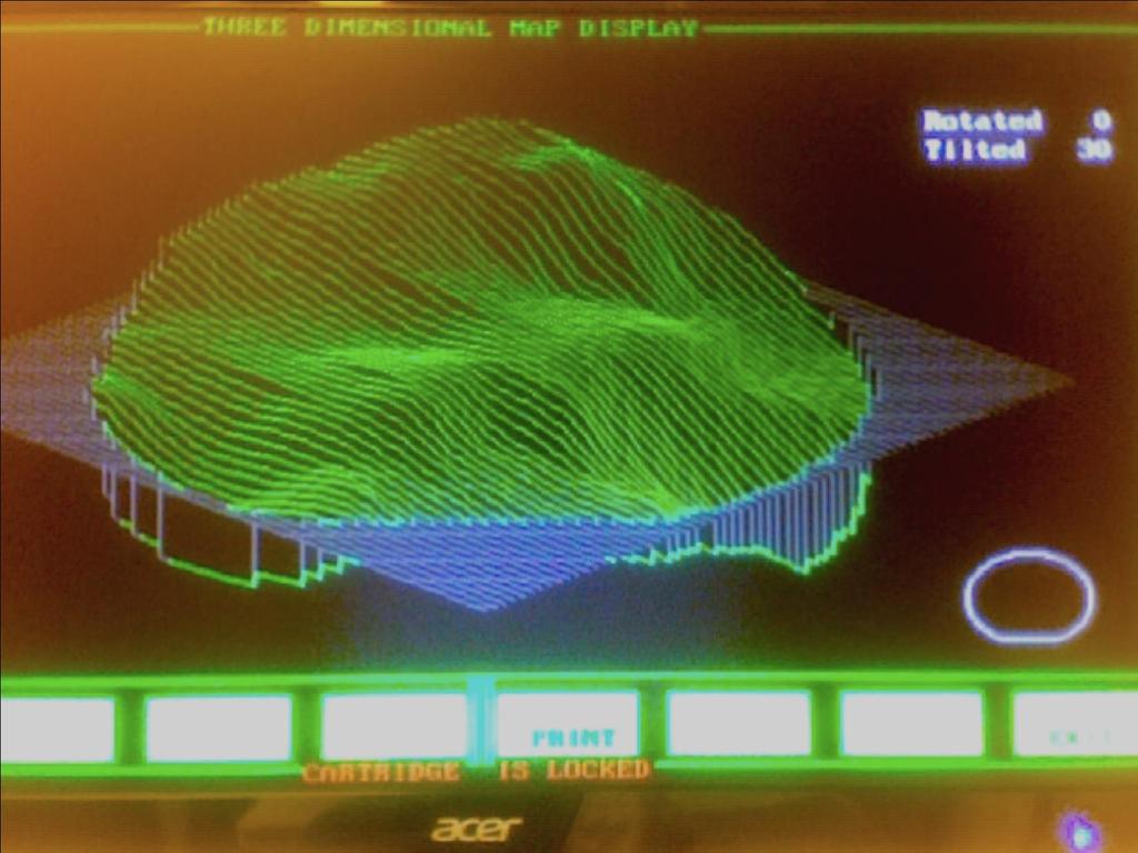
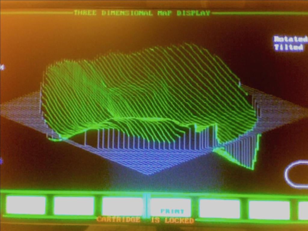
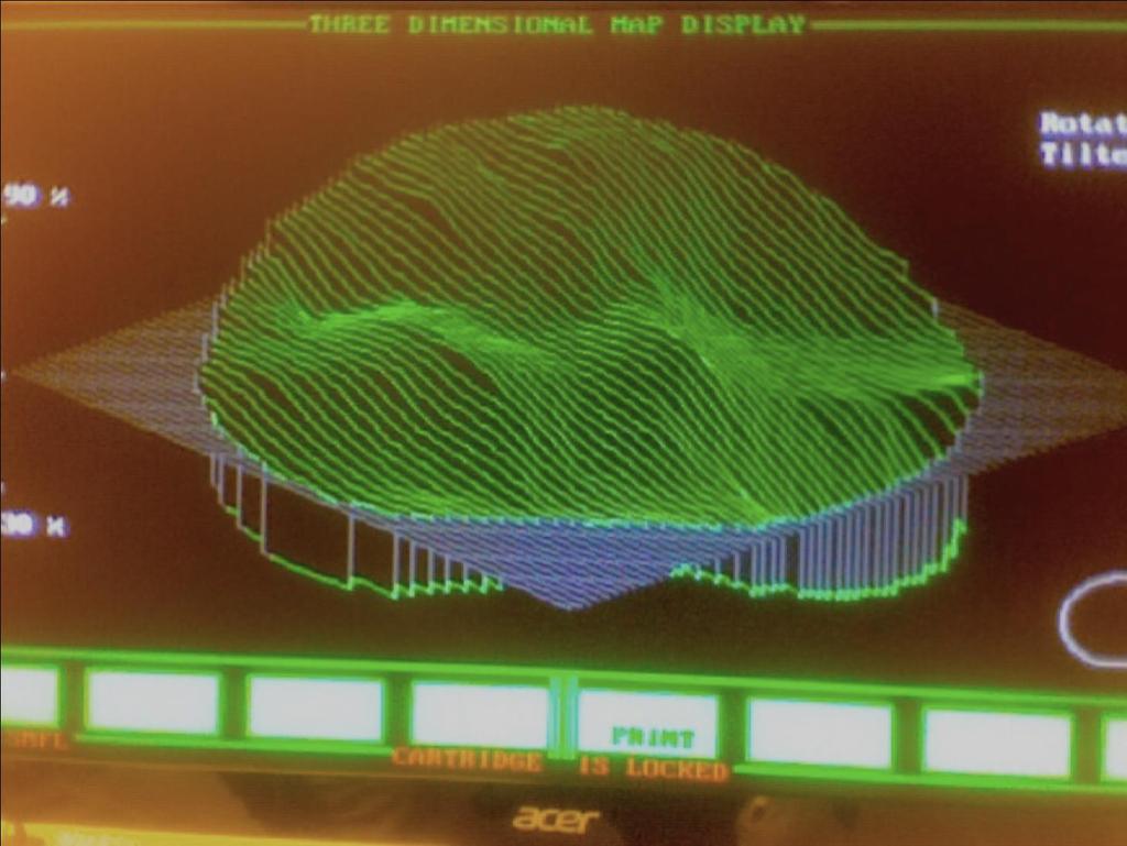
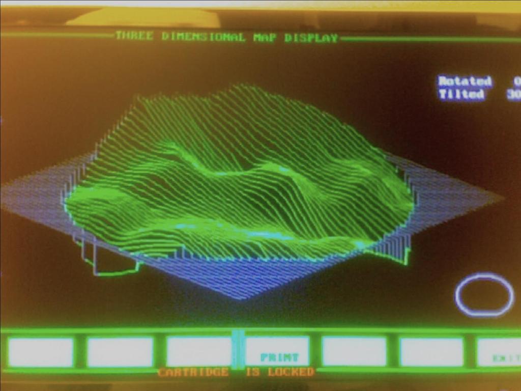
2 ABSTRACT This experiment explored the usage of oxygen gas in the Bruce furnace. Since oxygen gas is used often in the growth of silicon dioxide, a method for reducing the amount of oxygen used in the Bruce Furnace is desired to reduce cost. We began with a recipe for 500Angstroms of oxide using a dry oxide process on clean wafers. We ran the recipe using an oxygen flow rate of 10L/min and then 5L/min and compared both the thickness and uniformity of oxide growth on the wafers. We then ran a similar experiment with a recipe for 1000Angstroms of oxide. The results showed that cutting the oxygen flow rate (and thereby the cost of oxygen for each run) in half had no affect on oxide thickness and uniformity. 2
3 PROCEDURE Two bare wafers were placed in Tube 1 of the Bruce Furnace and recipe 250 was run for 500Angstroms of Dry Oxide. The wafers were measured with the Spectramap and data was recorded. The wafers were etched bare in BOE. Recipe 250 was altered, reducing the oxygen flow rate for the Soak period from 10L/min to 5L/min. The wafers were placed in Tube 1 and recipe 250, now altered, was run again. The wafers were measured with the Spectramap and data was recorded. Values for oxide thickness and uniformity were compared. 3
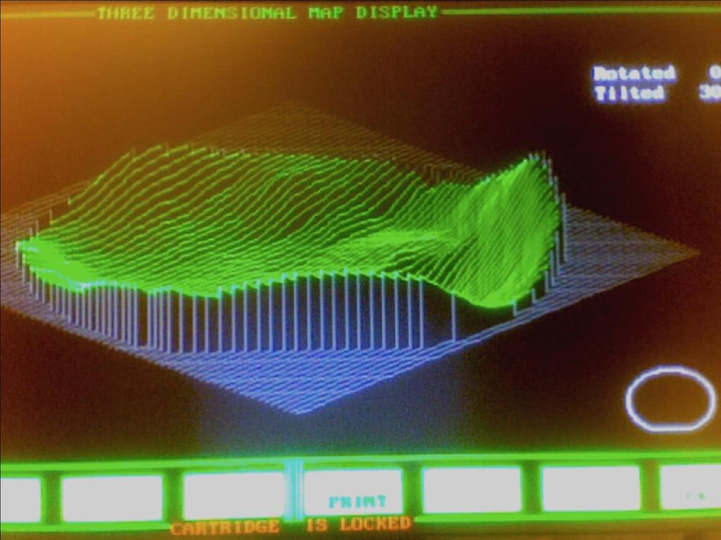
4 WAFER 1 RECIPE A 10L/MIN 1000C Mean: Standard Deviation: % Minimum: Maximum: Range: # Sites/Good: 81/80 4
5 5
6 WAFER 2 RECIPE A 10L/MIN 1000C Mean: Standard Deviation: % Minimum: Maximum: Range: # Sites/Good: 81/81 6
7 7
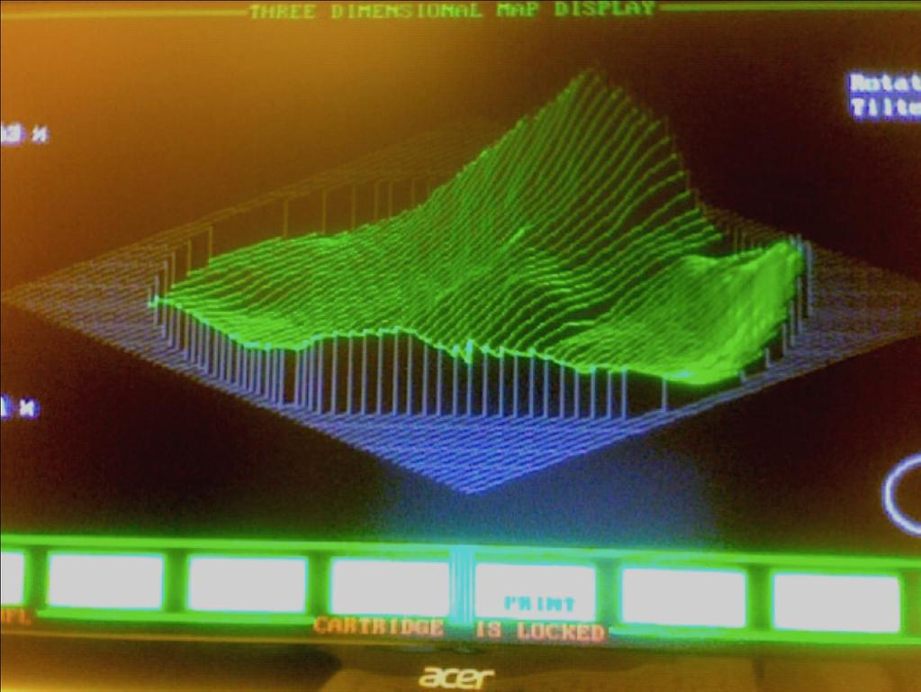
8 WAFER 1 RECIPE A 5L/MIN 1000C Mean: Standard Deviation: % Minimum: Maximum: Range: #Sites/Good: 81/81 8
9 9
10 WAFER 2 RECIPE A 5L/MIN 1000C Mean: Standard Deviation: % Minimum: Maximum: Range: #Sites/Good: 81/81 10
11 11
12 COMPARISON AND RESULTS 10L/min 5L/min 10L/min 5L/min Wafer 1 Wafer 1 Wafer 2 Wafer 2 Mean Standard Deviation % % % % Min Max Range #Sites/ Good 81/80 81/81 81/81 81/81 12
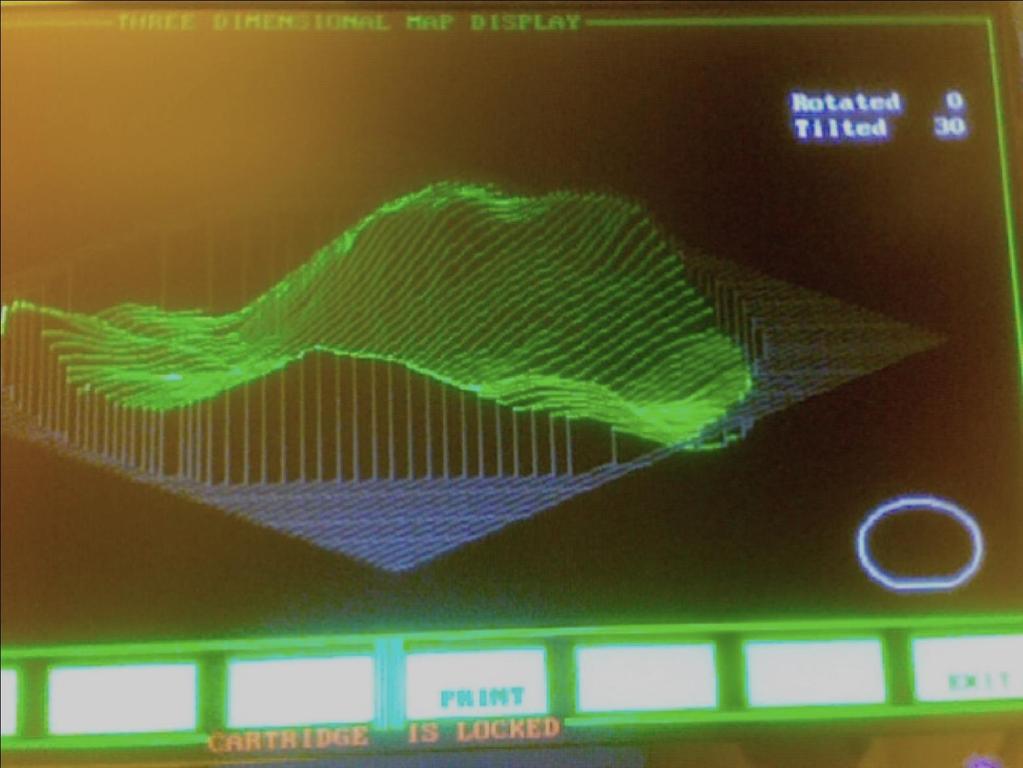
13 WAFER 1 RECIPE A 10L/MIN 1000C Mean: Standard Deviation: % Minimum: Maximum: Range: #Sites/Good: 81/81 13
14 14
15 WAFER 2 RECIPE A 10L/MIN 1000C Mean: Standard Deviation: % Minimum: Maximum: Range: #Sites/Good: 81/81 15
16 16
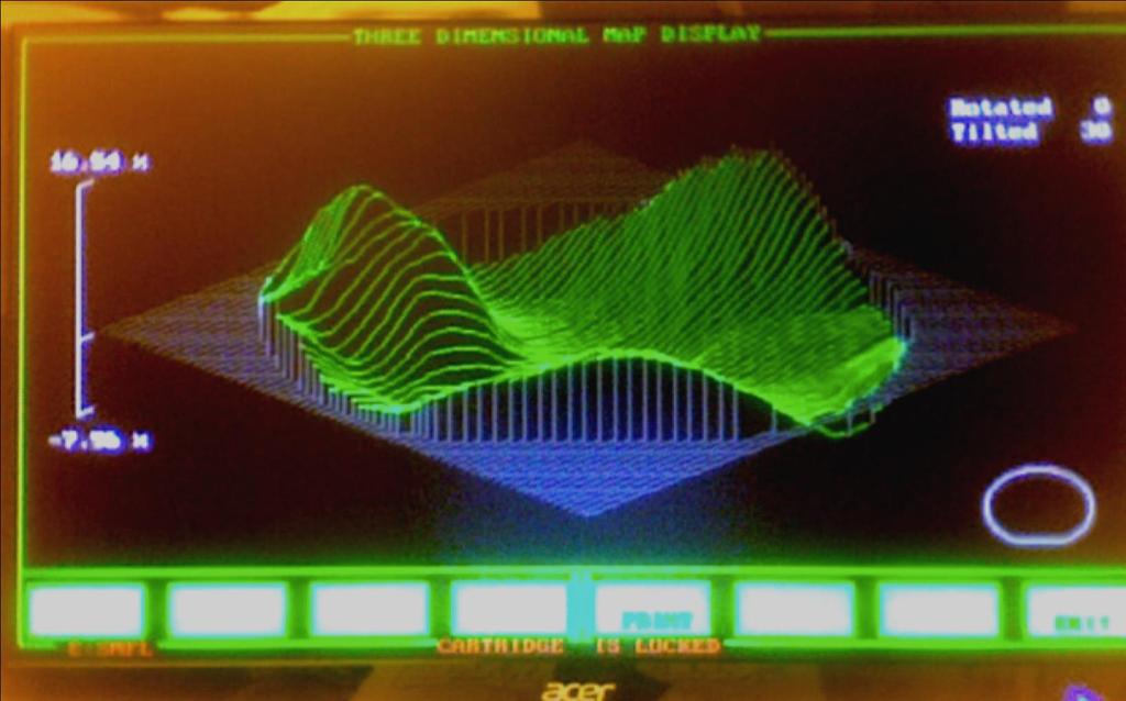
17 WAFER 1 RECIPE A 5L/MIN 1000C Mean: Standard Deviation: % Minimum: Maximum: Range: #Sites/Good: 81/81 17
18 18
19 WAFER 2 RECIPE A 5L/MIN 1000C Mean: Standard Deviation: % Minimum: Maximum: Range: #Sites/Good: 81/81 19
20 20
21 COMPARISON AND RESULTS 10L/min 5L/min 10L/min 5L/min Mean Standard Deviation % % % % Min Max Range #Sites/ Good 81/81 81/81 81/81 81/81 21
22 CALCULATIONS ENSURING SUFFICIENT QUANTITY OF OXYGEN GAS AVAILABLE Assume that 50 Wafers are present for a 500Angstrom oxide growth recipe, all wafers are coated uniformly, oxygen gas flows at 5L/min and is at STP upon entering Bruce Furnace. Si + O 2 SiO 2 SiO 2 Density: 2.65g/cm kg/m 3 SiO 2 Molar Mass: 60.08g/mol.06008kg/mol 22
23 MOLES O 2 NEEDED FOR 500A SIO 2 Volume SiO 2 Each Wafer V πr 2 h π(3in x (1cm/0.3937in) x (1m/100cm) ) 2 (500A x (10-10 m/1a)) x m 3 Mass SiO 2 Each Wafer Density = Mass/Volume Mass = (Density)(Volume) (2650kg/m 3 )(9.121 x m 3 ) = 6.65 x 10⁻⁷ kg Total Moles SiO 2 (50 Wafers) Moles = Mass/Molar Mass (6.65 x 10⁻⁷ kg /.06008kg/mol)(50 wafers) =5.535 x 10⁻⁴ mol SiO 2 Total Moles O 2 (50 Wafers) Si + O 2 SiO x 10-4 mol SiO 2 (1 mol O 2 / 1 mol SiO 2 ) x 10-4 mol O 2 necessary to grow 500A SiO 2 23
24 MOLES O 2 PROVIDED BY 500A SIO 2 RECIPE Liters of O 2 Used by Recipe (47 minutes)(5l/min) 235L Moles of O 2 Used by Recipe (235L O 2 )(1mol / 22.4L) mol O 2 provided 24
25 HOW MUCH EXCESS OXYGEN? (10.49 mol provided) / (5.535 x 10⁻⁴ mol needed) 19,000 times the necessary amount 25
26 CONCLUSION The data above shows that if the oxygen flow rate is reduced from 10L/min to 5L/min for a dry oxide growth process, it will not affect the thickness or uniformity of the oxide grown. Therefore, the oxygen usage can be reduced for dry oxide growth processes in recipes that use a 10L/min oxygen flow rate during the soak period. This could save approximately $2000 in cost every year. 26
27 REFERENCES Silicon VLSI Technology Fundamentals, Practice and Modeling. Plummer, Deal and Griffin 27
4. Thermal Oxidation. a) Equipment Atmospheric Furnace
 Equipment Atmospheric Furnace") 4. Thermal Oxidation a) Equipment Atmospheric Furnace Oxidation requires precise control of: temperature, T ambient gas, G time spent at any given T & G, t Vito Logiudice 34 4. Thermal Oxidation b) Mechanism
4. Thermal Oxidation a) Equipment Atmospheric Furnace Oxidation requires precise control of: temperature, T ambient gas, G time spent at any given T & G, t Vito Logiudice 34 4. Thermal Oxidation b) Mechanism
Plasma-Enhanced Chemical Vapor Deposition
 Plasma-Enhanced Chemical Vapor Deposition Steven Glenn July 8, 2009 Thin Films Lab 4 ABSTRACT The objective of this lab was to explore lab and the Applied Materials P5000 from a different point of view.
Rapid Thermal Processing (RTP) Dr. Lynn Fuller
 Dr. Lynn Fuller") ROCHESTER INSTITUTE OF TECHNOLOGY MICROELECTRONIC ENGINEERING Rapid Thermal Processing (RTP) Dr. Lynn Fuller Webpage: http://people.rit.edu/lffeee 82 Lomb Memorial Drive Rochester, NY 14623-5604 Tel (585)
ROCHESTER INSTITUTE OF TECHNOLOGY MICROELECTRONIC ENGINEERING Rapid Thermal Processing (RTP) Dr. Lynn Fuller Webpage: http://people.rit.edu/lffeee 82 Lomb Memorial Drive Rochester, NY 14623-5604 Tel (585)
Instructor: Dr. M. Razaghi. Silicon Oxidation
 SILICON OXIDATION Silicon Oxidation Many different kinds of thin films are used to fabricate discrete devices and integrated circuits. Including: Thermal oxides Dielectric layers Polycrystalline silicon
ALD Film Characterization Rachel Brown 5/13/14
 ALD Film Characterization Rachel Brown 5/13/14 Objective The following set of tests was performed to determine the characteristics of films created by the Atomic Layer system and how they varied with the
TANOS Charge-Trapping Flash Memory Structures
 TANOS Charge-Trapping Flash Memory Structures A Senior Design by Spencer Pringle 5/8/15 Table of Contents Motivation Why Charge-Trapping Flash (CTF)? Charge-Trapping vs. Floating Gate Electronically-Erasable
Chapter 2 Problems. The CMOS technology we need to realize is shown below, from Figure 1-34 in the text. S P + N P + N WELL P +
 Chapter 2 roblems 2.1 Sketch a process flow that would result in the structure shown in Figure 1-34 by drawing a series of drawings similar to those in this chapter. You only need to describe the flow
PDS Products PRODUCT DATA SHEET. BN-975 Wafers. Low Defect Boron Diffusion Systems. Features/Benefits BORON NITRIDE
 Low Defect Boron Diffusion Systems The purpose of the hydrogen injection process is to increase die yield per wafer. This is accomplished because the effects associated with the hydrogen injection process.
Process Flow in Cross Sections
 Process Flow in Cross Sections Process (simplified) 0. Clean wafer in nasty acids (HF, HNO 3, H 2 SO 4,...) --> wear gloves! 1. Grow 500 nm of SiO 2 (by putting the wafer in a furnace with O 2 2. Coat
Summary of Selected EMCR732 Projects for Spring 2005 Mike Aquilino Dr. Lynn Fuller
 ROCHESTER INSTITUTE OF TECHNOLOGY MICROELECTRONIC ENGINEERING Summary of Selected EMCR732 Projects for Spring 2005 Mike Aquilino Dr. Lynn Fuller Motorola Professor 82 Lomb Memorial Drive Rochester, NY
The Relation of Temperature Distribution on Silicon Wafer with Furnace Temperature and Gas Flow During Thermal Dry Oxidation Process
 The Relation of Temperature Distribution on Silicon Wafer with Furnace Temperature and Gas Flow During Thermal Dry Oxidation Process A.H. Azman 1, a *, S. Norhafiezah 2, b, RM Ayub 3, c, M. K. Md Arshad
Wafer Cleaning and Oxide Growth Laboratory Dr. Lynn Fuller Webpage:
 ROCHESTER INSTITUTE OF TECHNOLOGY MICROELECTRONIC ENGINEERING Wafer Cleaning and Oxide Growth Laboratory Dr. Lynn Fuller Webpage: http://www.rit.edu/~lffeee 82 Lomb Memorial Drive Rochester, NY 14623-5604
LAM 490 Etch Recipes. Dr. Lynn Fuller
 ROCHESTER INSTITUTE OF TECHNOLOGY MICROELECTRONIC ENGINEERING LAM 490 Etch Recipes Dr. Lynn Fuller Professor, Webpage: http://people.rit.edu/lffeee 82 Lomb Memorial Drive Rochester, NY 14623-5604 Tel (585)
Introduction to CMOS VLSI Design. Layout, Fabrication, and Elementary Logic Design
 Introduction to CMOS VLSI Design Layout, Fabrication, and Elementary Logic Design CMOS Fabrication CMOS transistors are fabricated on silicon wafer Lithography process similar to printing press On each
concentration of acid in mol / dm 3 temperature / C ti / min
 1 (a A small piece of marble, calcium carbonate, was added to 5 cm 3 of hydrochloric acid at 25 C. The time taken for the reaction to stop was measured. CaCO 3 (s) + 2HCl(aq) CaCl 2 (aq) + CO 2 (g) + H
Edinburgh Microfabrication Facility, University of Edinburgh.
 405 CONTROL OF OXIDE GROWTH BY REAL-TIME SIMULATION E. Cameron, J. Robertson, R. Holwill Edinburgh Microfabrication Facility, University of Edinburgh. SUMMARY As critical device features are reduced in
MEMS Surface Fabrication
 ROCHESTER INSTITUTE OF TECHNOLOGY MICROELECTRONIC ENGINEERING MEMS Surface Fabrication Dr. Lynn Fuller webpage: http://people.rit.edu/lffeee Electrical and Microelectronic Engineering Rochester Institute
CMOS Fabrication. Dr. Bassam Jamil. Adopted from slides of the textbook
 CMOS Fabrication Dr. Bassam Jamil Adopted from slides of the textbook CMOS Fabrication CMOS transistors are fabricated on silicon wafer Lithography process similar to printing press On each step, different
Oxide Growth. 1. Introduction
 Oxide Growth 1. Introduction Development of high-quality silicon dioxide (SiO2) has helped to establish the dominance of silicon in the production of commercial integrated circuits. Among all the various
Summary of Selected EMCR650/731 Projects for Jeremiah Hebding Dr. Lynn Fuller
 ROCHESTER INSTITUTE OF TECHNOLOGY MICROELECTRONIC ENGINEERING Summary of Selected EMCR650/731 Projects for 2004-2005 Jeremiah Hebding Dr. Lynn Fuller Motorola Professor 82 Lomb Memorial Drive Rochester,
Lab #2 Wafer Cleaning (RCA cleaning)
") Lab #2 Wafer Cleaning (RCA cleaning) RCA Cleaning System Used: Wet Bench 1, Bay1, Nanofabrication Center Chemicals Used: H 2 O : NH 4 OH : H 2 O 2 (5 : 1 : 1) H 2 O : HF (10 : 1) H 2 O : HCl : H 2 O 2
Lab #2 Wafer Cleaning (RCA cleaning) RCA Cleaning System Used: Wet Bench 1, Bay1, Nanofabrication Center Chemicals Used: H 2 O : NH 4 OH : H 2 O 2 (5 : 1 : 1) H 2 O : HF (10 : 1) H 2 O : HCl : H 2 O 2
University of Texas Arlington Department of Electrical Engineering. Nanotechnology Microelectromechanical Systems Ph.D. Diagnostic Examination
 University of Texas Arlington Department of Electrical Engineering Nanotechnology Microelectromechanical Systems Ph.D. Diagnostic Examination Fall 2012 November 17, 2012 Question # 1 2 3 To be filled by
This Appendix discusses the main IC fabrication processes.
 IC Fabrication B B.1 Introduction This Appendix discusses the main IC fabrication processes. B.2 NMOS fabrication NMOS transistors are formed in a p-type substrate. The NMOS fabrication process requires
CHAPTER 4: Oxidation. Chapter 4 1. Oxidation of silicon is an important process in VLSI. The typical roles of SiO 2 are:
 Chapter 4 1 CHAPTER 4: Oxidation Oxidation of silicon is an important process in VLSI. The typical roles of SiO 2 are: 1. mask against implant or diffusion of dopant into silicon 2. surface passivation
Why silicon? Silicon oxide
 Oxidation Layering. Oxidation layering produces a thin layer of silicon dioxide, or oxide, on the substrate by exposing the wafer to a mixture of highpurity oxygen or water at ca. 1000 C (1800 F). Why
ABSTRACT. which indicates the implanted region did not adequately inhibit the diffusion of oxygen.
 . INVESTIGATION OF LOCOS PROCESS USING NITROGEN IMPL~NTAT ION Joseph W. Walters 5th Year Microelectronic Engineering Student Rochester Institute of Technology INTRODUCTION ABSTRACT A localized oxidation
Microelectronic Device Instructional Laboratory. Table of Contents
 Introduction Process Overview Microelectronic Device Instructional Laboratory Introduction Description Flowchart MOSFET Development Process Description Process Steps Cleaning Solvent Cleaning Photo Lithography
HW 6 (Due Nov. 14, 2017)
") HW 6 (Due Nov. 14, 2017) Name: HW 6.1. The thickness of a plastic film (in mils) on a substrate material is thought to be influenced by the temperature at which the coating is applied. In completely randomized
HW 6 (Due Nov. 14, 2017) Name: HW 6.1. The thickness of a plastic film (in mils) on a substrate material is thought to be influenced by the temperature at which the coating is applied. In completely randomized
X-Ray Reflectivity Study of Hafnium Silicate Thin Films Prepared by Thermal Chemical Vapor Deposition
 X-Ray Reflectivity Study of Hafnium Silicate Thin Films Prepared by Thermal Chemical Vapor Deposition Hideyuki YAMAZAKI, Advanced LSI Technology Laboratory, Toshiba Corporation hideyuki.yamazaki@toshiba.co.jp
Semiconductor Manufacturing Technology. Semiconductor Manufacturing Technology
 Semiconductor Manufacturing Technology Michael Quirk & Julian Serda October 2001 by Prentice Hall Chapter 10 Oxidation 2001 2000 by Prentice Hall Diffusion Area of Wafer Fabrication Wafer fabrication (front-end)
Microelectronics. Integrated circuits. Introduction to the IC technology M.Rencz 11 September, Expected decrease in line width
 Microelectronics Introduction to the IC technology M.Rencz 11 September, 2002 9/16/02 1/37 Integrated circuits Development is controlled by the roadmaps. Self-fulfilling predictions for the tendencies
Oxidation SMT Yau - 1
 Oxidation Yau - 1 Objectives After studying the material in this chapter, you will be able to: 1. Describe an oxide film for semiconductor manufacturing, including its atomic structure, how it is used
All fabrication was performed on Si wafers with 285 nm of thermally grown oxide to
 Supporting Information: Substrate preparation and SLG growth: All fabrication was performed on Si wafers with 285 nm of thermally grown oxide to aid in visual inspection of the graphene samples. Prior
Bulk MEMS Fabrication Blog 2017 Dr. Lynn Fuller, Casey Gonta, Patsy Cadareanu
 ROCHESTER INSTITUTE OF TECHNOLOGY MICROELECTRONIC ENGINEERING Bulk MEMS Fabrication Blog 2017 Dr. Lynn Fuller, Casey Gonta, Patsy Cadareanu Webpage: http://people.rit.edu/lffeee 82 Lomb Memorial Drive
Thermal Oxidation and Growth of Insulators (Chapter 3 - Jaeger 3) Key advantage of Si: Oxidation of Si into SiO 2 (glass) Major factor in making
 Key advantage of Si: Oxidation of Si into SiO 2 (glass) Major factor in making") Thermal Oxidation and Growth of Insulators (Chapter 3 - Jaeger 3) Key advantage of Si: Oxidation of Si into SiO (glass) Major factor in making Silicon the main semiconductor Grown at high temperature in
Thermal Oxidation and Growth of Insulators (Chapter 3 - Jaeger 3) Key advantage of Si: Oxidation of Si into SiO (glass) Major factor in making Silicon the main semiconductor Grown at high temperature in
Ultra High Barrier Coatings by PECVD
 Society of Vacuum Coaters 2014 Technical Conference Presentation Ultra High Barrier Coatings by PECVD John Madocks & Phong Ngo, General Plasma Inc., 546 E. 25 th Street, Tucson, Arizona, USA Abstract Silicon
Ultrathin oxynitride formation by low energy ion implantation
 Ultrathin oxynitride formation by low energy ion implantation A. Khoueir and Z. H. Lu Department of Metallurgy and Materials Science, University of Toronto, Toronto, Ontario M5S 3E4, Canada W. T. Ng Department
Process Improvement Projects May 2006 Dr. Lynn Fuller
 ROCHESTER INSTITUTE OF TECHNOLOGY MICROELECTRONIC ENGINEERING Process Improvement Projects May 2006 Dr. Lynn Fuller 82 Lomb Memorial Drive Rochester, NY 14623-5604 Tel (585) 475-2035 Fax (585) 475-5041
Cobalt Silicide Formation and Patterning Technology
 Cobalt Silicide Formation and Patterning Technology Neil S. Patel Microelectronic Engineering Rochester Institute of Technology Rochester, NY 14623 Abstract The goal of this investigation was to develop
Report 1. B. Starting Wafer Specs Number: 10 Total, 6 Device and 4 Test wafers
 Aaron Pederson EE 432 Lab Dr. Meng Lu netid: abp250 Lab instructor: Yunfei Zhao Report 1 A. Overview The goal of this lab is to go through the semiconductor fabrication process from start to finish. This
VLSI Systems and Computer Architecture Lab
 ΚΥΚΛΩΜΑΤΑ VLSI Πανεπιστήμιο Ιωαννίνων CMOS Technology Τμήμα Μηχανικών Η/Υ και Πληροφορικής 1 From the book: An Introduction ti to VLSI Process By: W. Maly ΚΥΚΛΩΜΑΤΑ VLSI Διάρθρωση 1. N well CMOS 2. Active
Isolation Technology. Dr. Lynn Fuller
 ROCHESTER INSTITUTE OF TECHNOLOGY MICROELECTRONIC ENGINEERING Isolation Technology Dr. Lynn Fuller Motorola Professor 82 Lomb Memorial Drive Rochester, NY 14623-5604 Tel (585) 475-2035 Fax (585) 475-5041
Bulk MEMS Fabrication Details Dr. Lynn Fuller, Casey Gonta, Patsy Cadareanu
 ROCHESTER INSTITUTE OF TECHNOLOGY MICROELECTRONIC ENGINEERING Bulk MEMS Fabrication Details Dr. Lynn Fuller, Casey Gonta, Patsy Cadareanu Webpage: http://people.rit.edu/lffeee 82 Lomb Memorial Drive Rochester,
Increased Yield Using PDS Products Grade BN-975 with Hydrogen Injection
 Increased Yield Using PDS Products Grade BN-975 with Hydrogen Injection Technical Bulletin The purpose of the hydrogen injection process is to increase die yield per wafer. This is accomplished because
Colorado School of Mines PHGN/CHGN 435. Modules 1 and 2. Authors: Garrick Johnson Trevor Haak Carl DuBois Ethan Palay
 Colorado School of Mines PHGN/CHGN 435 Modules 1 and 2 Authors: Garrick Johnson Trevor Haak Carl DuBois Ethan Palay February 10, 2015 1 Introduction and Background Integrated circuits are an integral part
MATERIALS. Silicon Wafers... J 04 J 01. MATERIALS / Inorganics & thin films guide
 J MATERIALS SUBSTRATES Silicon Wafers... J 04 J J 01 MATERIALS SUBSTRATES NEYCO has a complete range of crystal substrates for a wide variety of applications, including Semiconductor, Biotechnology, Nanotechnology,
Lab 1: Field Oxide. Overview. Starting Wafers
 Overview Lab 1: Field Oxide Brandon Baxter, Robert Buckley, Tara Mina, Quentin Vingerhoets Lab instructor: Liang Zhang Course Instructor: Dr. Gary Tuttle EE 432-532 January 23, 2017 In this lab we created
EE432/532 CYMOS PROCESS PWELL LITHOGRAPHY AND DIFFUSION
 EE432/532 CYMOS PROCESS PWELL LITHOGRAPHY AND DIFFUSION [Document subtitle] GROUP 4 GROUP 4 (TUESDAY AFTERNOON) GROUP LEADER: ANDREW MCNEIL GROUP MEMBERS: WENG HOONG LOO MARIO PEREZ ZHIHAO LIAO LAB INSTRUCTOR
MICROCHIP MANUFACTURING by S. Wolf
 MICROCHIP MANUFACTURING by S. Wolf Chapter 13: THERMAL- OXIDATION of SILICON 2004 by LATTICE PRESS Chapter 13: THERMAL-OXIDATION of SILICON n CHAPTER CONTENTS Applications of Thermal Silicon-Dioxide Physical
micro resist technology
 Characteristics Processing guidelines Negative Tone Photoresist Series ma-n 2400 ma-n 2400 is a negative tone photoresist series designed for the use in micro- and nanoelectronics. The resists are available
A discussion of crystal growth, lithography, etching, doping, and device structures is presented in
 Chapter 5 PROCESSING OF DEVICES A discussion of crystal growth, lithography, etching, doping, and device structures is presented in the following overview gures. SEMICONDUCTOR DEVICE PROCESSING: AN OVERVIEW
Midterm evaluations. Nov. 9, J/3.155J 1
 Midterm evaluations What learning activities were found most helpful Example problems, case studies (5); graphs (good for extracting useful info) (4); Good interaction (2); Good lecture notes, slides (2);
Selective-Area Atomic Layer Deposition (SA-ALD) of Titanium Dioxide (TiO 2) using Poly(methyl methacrylate) (PMMA) Michael Tu 5/12/2016
 of Titanium Dioxide (TiO 2) using Poly(methyl methacrylate) (PMMA) Michael Tu 5/12/2016") Selective-Area Atomic Layer Deposition (SA-ALD) of Titanium Dioxide (TiO 2) using Poly(methyl methacrylate) (PMMA) Michael Tu 5/12/2016 Introduction The Minnesota Nano Center s Keller Hall facility includes
Selective-Area Atomic Layer Deposition (SA-ALD) of Titanium Dioxide (TiO 2) using Poly(methyl methacrylate) (PMMA) Michael Tu 5/12/2016 Introduction The Minnesota Nano Center s Keller Hall facility includes
2015 EE410-LOCOS 0.5µm Poly CMOS Process Run Card Lot ID:
 STEP 0.00 - PHOTOMASK #0- ZERO LEVEL MARKS Starting materials is n-type silicon (5-10 ohm-cm). Add four test wafers labeled T1-T4. T1 and T2 will travel with the device wafers and get all of the processing
Section 4: Thermal Oxidation. Jaeger Chapter 3. EE143 - Ali Javey
 Section 4: Thermal Oxidation Jaeger Chapter 3 Properties of O Thermal O is amorphous. Weight Density =.0 gm/cm 3 Molecular Density =.3E molecules/cm 3 O Crystalline O [Quartz] =.65 gm/cm 3 (1) Excellent
CMP Process Development for Shallow Trench Isolation (STI)
") CMP Process Development for Shallow Trench Isolation (STI) Robert A. Seifridge Microelectronic Engineering Rochester Institute of Technology Rochester, NY 14623 Abstract Tool characterization and optimization
CMP Process Development for Shallow Trench Isolation (STI) Robert A. Seifridge Microelectronic Engineering Rochester Institute of Technology Rochester, NY 14623 Abstract Tool characterization and optimization
Brian Izzio 5th Year Microelectronic Engineering Student. Rochester Institute of Technology
 CAPACITAWZE-VOI~TAGE characterization FOR POLYSILICON GATE MOS CAPACITORS DJTRODUcTION Brian Izzio 5th Year Microelectronic Engineering Student Rochester Institute of Technology ABSTRACT The effects of
EFFECT OF CRYSTALORIENTATIONIN OXIDATION PROCESS OF VLSI FABRICATION
 International Journal of Research in Engineering, Technology and Science, Volume VII, Special Issue, Feb 2017 www.ijrets.com, editor@ijrets.com, ISSN 2454-1915 EFFECT OF CRYSTALORIENTATIONIN OXIDATION
CMOS FABRICATION. n WELL PROCESS
 CMOS FABRICATION n WELL PROCESS Step 1: Si Substrate Start with p- type substrate p substrate Step 2: Oxidation Exposing to high-purity oxygen and hydrogen at approx. 1000 o C in oxidation furnace SiO
VLSI Technology. By: Ajay Kumar Gautam
 By: Ajay Kumar Gautam Introduction to VLSI Technology, Crystal Growth, Oxidation, Epitaxial Process, Diffusion Process, Ion Implantation, Lithography, Etching, Metallization, VLSI Process Integration,
Bruce Furnace Recipes Dr. Lynn Fuller Webpage: Electrical and Microelectronic Engineering
 ROCHESTER INSTITUTE OF TECHNOLOGY MICROELECTRONIC ENGINEERING Bruce Furnace Recipes Dr. Lynn Fuller Webpage: http://people.rit.edu/lffeee Electrical and 82 Lomb Memorial Drive Rochester, NY 14623-5604
ECE 440 Lecture 27 : Equilibrium P-N Junctions I Class Outline:
 ECE 440 Lecture 27 : Equilibrium P-N Junctions I Class Outline: Fabrication of p-n junctions Contact Potential Things you should know when you leave Key Questions What are the necessary steps to fabricate
Processing guidelines. Negative Tone Photoresist Series ma-n 2400
 Characteristics Processing guidelines Negative Tone Photoresist Series ma-n 2400 ma-n 2400 is a negative tone photoresist series designed for the use in micro- and nanoelectronics. The resists are available
Crystal Growth and Wafer Fabrication. K.Sivasankaran, Assistant Professor (Senior), VLSI Division, School of Electronics Engineering, VIT
, VLSI Division, School of Electronics Engineering, VIT") Crystal Growth and Wafer Fabrication K.Sivasankaran, Assistant Professor (Senior), VLSI Division, School of Electronics Engineering, VIT Crystal growth Obtaining sand Raw Polysilicon Czochralski Process
Crystal Growth and Wafer Fabrication K.Sivasankaran, Assistant Professor (Senior), VLSI Division, School of Electronics Engineering, VIT Crystal growth Obtaining sand Raw Polysilicon Czochralski Process
Etching Etching Definitions Isotropic Etching: same in all direction Anisotropic Etching: direction sensitive Selectivity: etch rate difference
 Etching Etching Definitions Isotropic Etching: same in all direction Anisotropic Etching: direction sensitive Selectivity: etch rate difference between 2 materials Need strong selectivity from masking
EECS130 Integrated Circuit Devices
 EECS130 Integrated Circuit Devices Professor Ali Javey 9/13/2007 Fabrication Technology Lecture 1 Silicon Device Fabrication Technology Over 10 15 transistors (or 100,000 for every person in the world)
EE143 Microfabrication Technology Fall 2009 Homework #2 - Answers
 EE143 Microfabrication Technology Fall 2009 Homework #2 - Answers Note: If you are asked to plot something on this homework or any future homework, make an accurate plot using Excel, Matlab, etc., with
CyMOS process Spring 2016 Iowa State University
 CyMOS process Spring 2016 Iowa State University Start Date Starting Material Orientation: Dopant: Resistivity: Ω cm Doping Concentration: cm 3 Diameter: inch Thickness: µm Lot Identification: Wafer Count
5.8 Diaphragm Uniaxial Optical Accelerometer
 5.8 Diaphragm Uniaxial Optical Accelerometer Optical accelerometers are based on the BESOI (Bond and Etch back Silicon On Insulator) wafers, supplied by Shin-Etsu with (100) orientation, 4 diameter and
Today s Class. Materials for MEMS
 Lecture 2: VLSI-based Fabrication for MEMS: Fundamentals Prasanna S. Gandhi Assistant Professor, Department of Mechanical Engineering, Indian Institute of Technology, Bombay, Recap: Last Class What is
KGC SCIENTIFIC Making of a Chip
 KGC SCIENTIFIC www.kgcscientific.com Making of a Chip FROM THE SAND TO THE PACKAGE, A DIAGRAM TO UNDERSTAND HOW CPU IS MADE? Sand CPU CHAIN ANALYSIS OF SEMICONDUCTOR Material for manufacturing process
Semiconductor Technology
 Semiconductor Technology from A to Z Oxidation www.halbleiter.org Contents Contents List of Figures List of Tables II III 1 Oxidation 1 1.1 Overview..................................... 1 1.1.1 Application...............................
FABRICATION OF CMOS INTEGRATED CIRCUITS. Dr. Mohammed M. Farag
 FABRICATION OF CMOS INTEGRATED CIRCUITS Dr. Mohammed M. Farag Outline Overview of CMOS Fabrication Processes The CMOS Fabrication Process Flow Design Rules EE 432 VLSI Modeling and Design 2 CMOS Fabrication
R Sensor resistance (Ω) ρ Specific resistivity of bulk Silicon (Ω cm) d Diameter of measuring point (cm)
 ρ Specific resistivity of bulk Silicon (Ω cm) d Diameter of measuring point (cm)") 4 Silicon Temperature Sensors 4.1 Introduction The KTY temperature sensor developed by Infineon Technologies is based on the principle of the Spreading Resistance. The expression Spreading Resistance derives
4 Silicon Temperature Sensors 4.1 Introduction The KTY temperature sensor developed by Infineon Technologies is based on the principle of the Spreading Resistance. The expression Spreading Resistance derives
Chapter 3. In this chapter, we use sol-gel method to combine three high-k precursors, i.e. HfCl 4, ZrCl 4 and SiCl 4 together to form hafnium silicate
 Chapter 3 Sol-Gel-Derived Zirconium Silicate (ZrSi x O y ) and Hafnium Silicate (HfSi x O y ) Co-existed Nanocrystal SONOS Memory 3-1 Introduction In the previous chapter, we fabricate the sol-gel-derived
PRIME WATER PRODUCTS 11-ELECTRODES CELL FEATURES. Website :
 PRIME WATER PRODUCTS 11-ELECTRODES CELL FEATURES Website : www.primewater.co.kr New Larger 11 Platinum Titanium New Larger 11 Platinum Titanium Plates New Larger Ultra Efficient Multi-Level Electrolysis
A Deep Silicon RIE Primer Bosch Etching of Deep Structures in Silicon
 A Deep Silicon RIE Primer Bosch Etching of Deep Structures in Silicon April 2009 A Deep Silicon RIE Primer 1.0) Etching: Silicon does not naturally etch anisotropically in fluorine based chemistries. Si
Chapter 2 Manufacturing Process
 Digital Integrated Circuits A Design Perspective Chapter 2 Manufacturing Process 1 CMOS Process 2 CMOS Process (n-well) Both NMOS and PMOS must be built in the same silicon material. PMOS in n-well NMOS
Test Patterns for Chemical Mechanical Polish Characterization
 Dobek S: CMP Characterization 15th Annual Microelectronic Engineering Conference, 1997 Test Patterns for Chemical Mechanical Polish Characterization Stanley 3. Dobek Senior Microelectronic Engineering
IC/MEMS Fabrication - Outline. Fabrication
 IC/MEMS Fabrication - Outline Fabrication overview Materials Wafer fabrication The Cycle: Deposition Lithography Etching Fabrication IC Fabrication Deposition Spin Casting PVD physical vapor deposition
Chapter 4. UEEP2613 Microelectronic Fabrication. Oxidation
 Chapter 4 UEEP2613 Microelectronic Fabrication Oxidation Prepared by Dr. Lim Soo King 24 Jun 2012 Chapter 4...113 Oxidation...113 4.0 Introduction... 113 4.1 Chemistry of Silicon Dioxide Formation... 115
Surface Micromachining
 Surface Micromachining Micro Actuators, Sensors, Systems Group University of Illinois at Urbana-Champaign Outline Definition of surface micromachining Most common surface micromachining materials - polysilicon
3.155J / 6.152J MICROELECTRONICS PROCESSING TECHNOLOGY TAKE-HOME QUIZ FALL TERM 2003
 3.155J / 6.152J MICROELECTRONICS PROCESSING TECHNOLOGY TAKE-HOME QUIZ FALL TERM 2003 1) This is an open book, take-home quiz. You are not to consult with other class members or anyone else. You may discuss
Figure 2.3 (cont., p. 60) (e) Block diagram of Pentium 4 processor with 42 million transistors (2000). [Courtesy Intel Corporation.
 (e) Block diagram of Pentium 4 processor with 42 million transistors (2000). [Courtesy Intel Corporation.") Figure 2.1 (p. 58) Basic fabrication steps in the silicon planar process: (a) oxide formation, (b) selective oxide removal, (c) deposition of dopant atoms on wafer, (d) diffusion of dopant atoms into exposed
Figure 2.1 (p. 58) Basic fabrication steps in the silicon planar process: (a) oxide formation, (b) selective oxide removal, (c) deposition of dopant atoms on wafer, (d) diffusion of dopant atoms into exposed
LAM4600 Plasma Etch Tool Recipes Dr. Lynn Fuller
 ROCHESTER INSTITUTE OF TECHNOLOGY MICROELECTRONIC ENGINEERING LAM4600 Plasma Etch Tool Recipes Dr. Lynn Fuller Webpage: http://people.rit.edu/lffeee 82 Lomb Memorial Drive Rochester, NY 14623-5604 Tel
Selective Oxidation of Advanced High Strength Steels (AHSS) and Ultra High Strength Steel (UHSS) Utilizing Direct Fired Burners
 and Ultra High Strength Steel (UHSS) Utilizing Direct Fired Burners") Selective Oxidation of Advanced High Strength Steels (AHSS) and Ultra High Strength Steel (UHSS) Utilizing Direct Fired Burners Scott Brown 1, David Schalles 2, Frank Beichner 3 1 Director of Sales and
Selective Oxidation of Advanced High Strength Steels (AHSS) and Ultra High Strength Steel (UHSS) Utilizing Direct Fired Burners Scott Brown 1, David Schalles 2, Frank Beichner 3 1 Director of Sales and
HYPRES. Hypres MCM Process Design Rules 04/12/2016
 HYPRES Hypres MCM Process Design Rules 04/12/2016 Direct all inquiries, questions, comments and suggestions concerning these design rules and/or HYPRES fabrication to: Daniel T. Yohannes Tel. (914) 592-1190
Chapter 5: REACTION SINTERING of diamond and silicon powders
 Chapter 5: REACTION SINTERING of diamond and silicon powders In this chapter are presented the results, discussion and conclusion on preparation of the diamond-silicon carbide composite by reaction sintering
TOWARD MEMS!Instructor: Riadh W. Y. Habash
 TOWARD MEMS!Instructor: Riadh W. Y. Habash Students are presented with aspects of general production and manufacturing of integrated circuit (IC) products to enable them to better liaise with and participate
3.155J / 6.152J Micro/Nano Processing Technology TAKE-HOME QUIZ FALL TERM 2005
 3.155J / 6.152J Micro/Nano Processing Technology TAKE-HOME QUIZ FALL TERM 2005 1) This is an open book, take-home quiz. You are not to consult with other class members or anyone else. You may discuss the
Photoresist Coat, Expose and Develop Laboratory Dr. Lynn Fuller
 ROCHESTER INSTITUTE OF TECHNOLOGY MICROELECTRONIC ENGINEERING Photoresist Coat, Expose and Develop Laboratory Dr. Lynn Fuller Webpage: http://www.rit.edu/lffeee 82 Lomb Memorial Drive Rochester, NY 14623-5604
Chapter 2 MOS Fabrication Technology
 Chapter 2 MOS Fabrication Technology Abstract This chapter is concerned with the fabrication of metal oxide semiconductor (MOS) technology. Various processes such as wafer fabrication, oxidation, mask
EE 330 Lecture 9. IC Fabrication Technology Part II. -Oxidation -Epitaxy -Polysilicon -Planarization -Resistance and Capacitance in Interconnects
 EE 330 Lecture 9 IC Fabrication Technology Part II -Oxidation -Epitaxy -Polysilicon -Planarization -Resistance and Capacitance in Interconnects Review from Last Time IC Fabrication Technology Crystal Preparation
Drytech Quad Etch Recipes Dr. Lynn Fuller Mike Aquilino Microelectronic Engineering
 ROCHESTER INSTITUTE OF TECHNOLOGY MICROELECTRONIC ENGINEERING Drytech Quad Etch Recipes Dr. Lynn Fuller Mike Aquilino 82 Lomb Memorial Drive Rochester, NY 14623-5604 Tel (585) 475-2035 Fax (585) 475-5041
Chapter 3 Silicon Device Fabrication Technology
 Chapter 3 Silicon Device Fabrication Technology Over 10 15 transistors (or 100,000 for every person in the world) are manufactured every year. VLSI (Very Large Scale Integration) ULSI (Ultra Large Scale
PY2N20 Material Properties and Phase Diagrams
 PY2N20 Material Properties and Phase Diagrams Lecture 9 P. Stamenov, PhD School of Physics, TCD PY2N20-9 Semiconductor Wafer Production - Si Czochralski Growth Growth from melt Melt 99.999999% pure polycrystalline
EE 143 MICROFABRICATION TECHNOLOGY FALL 2014 C. Nguyen PROBLEM SET #9
 Issued: Tuesday, Nov. 11, 2014 PROLEM SET #9 Due: Wednesday, Nov. 19, 2010, 8:00 a.m. in the EE 143 homework box near 140 Cory 1. The following pages comprise an actual pwell CMOS process flow with poly-to-poly
Silicon Epitaxial CVD Want to create very sharp PN boundary grow one type layer on other in single crystal form High dopant layers on low dopant
 Silicon Epitaxial CVD Want to create very sharp PN boundary grow one type layer on other in single crystal form High dopant layers on low dopant substrate Creates latch up protection for CMOS Buried Epi
Silicon Manufacturing
 Silicon Manufacturing Group Members Young Soon Song Nghia Nguyen Kei Wong Eyad Fanous Hanna Kim Steven Hsu th Fundamental Processing Steps 1.Silicon Manufacturing a) Czochralski method. b) Wafer Manufacturing