Atomic Layer Deposition of High-k k Dielectric and Metal Gate Stacks for MOS Devices
|
|
|
- Stephen Stephens
- 6 years ago
- Views:
Transcription

1 International Conference on Characterization and Metrology for ULSI Technology March 15-18, 2005 Atomic Layer Deposition of High-k k Dielectric and Metal Gate Stacks for MOS Devices Yoshi Senzaki, Kisik Choi, Paul D. Kirsch, Prashant Majhi, Byoung Hun Lee SEMATECH, the SEMATECH logo, AMRC, Advanced Materials Research Center, ATDF, the ATDF logo, Advanced Technology Development Facility, ISMI and International SEMATECH Manufacturing Initiative are servicemarks of SEMATECH, Inc. All other servicemarks and trademarks are the property of their respective owners.
2 Outline 1. Introduction 2. ALD of High-k Dielectric High-k dielectric ALD processes Electrical properties of MOS devices Scaling the Hf-based dielectric 3. ALD of Metal Gate ALD Metal Nitrides - TiN, HfN, HfSiN, TaN Work function evaluation
3 MOSFET Device Goals for 45 nm node and beyond Application EOT (nm) CET (nm) Jg (A/cm 2 ) High Performance (HP) </= 0.8 </= 1.2 </= 100 Low Standby Power (LSTP) </= 1.6 </= 2.4 </= 2.2x10⁻³ Density of interface traps (D it ) </= 5x10 10 # / cm 2 ev High frequency (100kHz) CV hysteresis </= 10 mv V t ± 0.2V of control SiO 2 with same EOT V t stability ± 10mV of unstressed film Mobility >/= 90% of SiO 2 at EOT 0.8nm Defect Density </= 0.14 defects / cm 2 Thermal stability (physical and electrical) at 1000ºC, 5 sec Thickness uniformity (3 sigma) </= 4% Reliability comparable to SiO 2

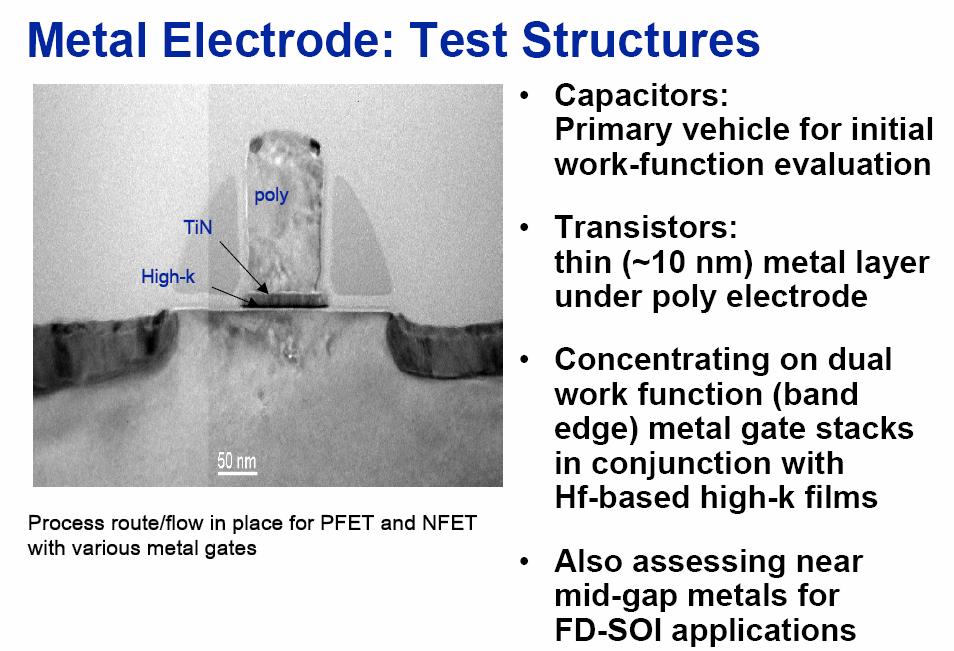
4 Factors That Influence Metal Electrode Properties Poly Why: Ease of integration Effect: Stress?, Reaction with electrode if no barrier layer? Why: prevent interaction between Electrode and Poly; Effect: Stress?, Reaction with metal electrode? Metal diffusion through electrode grain boundary and pile up at TIL? Overlay effect if electrode very thin? Barrier/Cap Layer Metal Electrode Top Interface Layer (TIL) Dielectric Why: Control WF, EOT scaling (no poly depln) Effect: main contributor to WF, Crystallinity, grain orientation, thickness effect? Overlay effect if TIL (intentional) very thin? Why: Unintentional (due to reaction of metal with dielectric); Intentional (dual metal integration and EWF control via overlay effect) Effect: controls EWF if TIL forms Bottom Interface Layer (BIL) Why: High-k for scaling Effect: reaction with metal to form TIL + Fermi level pinning, fixed charges shift Vfb shift.
5 Introduction: Why Metal ALD? Why metal electrodes? poly electrode depletion limits device scaling poly electrode can interact with high-k materials Why ALD metal electrodes? Excellent thin film thickness uniformity control Excellent composition control Little damage to gate oxide (compared to PVD) Low temperature deposition with low impurity Conformality at nanoscale structures and potentially 3-D devices Multiple potential applications for ALD metal films Metal gate electrode: TaN, TiN, W, Ru.. Cu diffusion barrier/adhesion promoter: TaN, Ta, TaSiN, TiN, WN.. Cu seed layer: Cu Plug for via hole: W, WN x Barrier: TiN, Ti
6 Gate ELECTRODE Specifications Application EWF (n metal) EWF (p metal) CMOS on bulk Si 4.1 +/ /-0.05 CMOS on FDSOI, FINFET 4.4 +/ /-0.05 Gate stack subjected to S/D dopant activation anneal (1000 C, 5 sec) V t ± 0.1 V of control SiO 2 with same EOT V t stability ± 10mV of unstressed film Mobility >/= 95% of SiO 2 Density of interface traps (D it ) </= 5x10 10 # / cm 2 ev High frequency (100kHz) CV hysteresis </= 10 mv Reliability comparable to Poly/SiO 2 Defect Density </= 0.14 defects / cm 2 Thickness uniformity (3 sigma) </= 4%
7 ALD Processes: Metal-Organic Liquid Precursors for HfO 2 Hf-t-Butoxide Hf(C 4 H 9 O) 4 Dep. Rate: 0.24Å/cycle TEMAHf (Tetrakisethylmethyl amino hafnium) Hf(NMeEt) 4 H 9 C 4 O H 9 C 4 O Hf OC 4 H 9 OC 4 H 9 Dep. Rate: 0.89Å/cycle Less impurities in the HfO 2 films Lower leakage current of HfO 2 --> Precursor of choice N Hf N ECS Proceedings, 2003 N N
8 Precursor Co-injection ALD Concept for HfSiOx A+B(g) Introduction of A+B(g) onto the substrate surface Introduction of A(g) + B(g) onto the substrate surface Formation of an A+B(s) monolayer surface A+B(S) Formation of an A+B(s) monolayer surface Introduction of C(g) onto A+B(s) surface C(g) Introduction of C(g) onto A+B(s) surface Formation of C(s) monolayer surface C(S) Formation of C(s) monolayer surface 8
9 HfSiOx ALD Precursors N N N N Hf Si Hf N N N N TEMAHf TEMASi Chemical compatibility -> suppresses gas phase reaction J. Vac. Sci. Technol. (A), vol. 22, p.1175 (2004).
10 HfSiO x ALD Coinjection vs Nano-laminate Precursor coinjection Hf/Si pulse/purge + Oxidizer pulse/purge Nano-laminate HfSiO x Si Hf pulse/purge + Ox pulse/purge + Si pulse/purge + Ox pulse/purge HfO 2 SiO 2 HfO 2 SiO 2 HfO 2 Si high temperature anneal HfSiO x Si
11 Leakage Current (J g ) Reduction of Hf(Si)O J g (V fb -1) [A/cm 2 ] HfO 2 HfSiO SiO 2 /PolySi EOT (Å) J g reduction: x vs. SiO 2 /PloySi
12 Mobility Progress with HfO 2 and HfSiO Mobility - 1MV/cm (cm 2 /V-s) Univ SiO 2 HfO2 HfSiO 140 HfO2 "B" 120 HfSiO "B" HfSiO "A" 100 HfO2 "A" SiON ref [4] 80 SiO2 ref EOT (Å) HfO 2 and HfSiO show mobility results similar to nitrided oxide Significant improvement relative to historical dataset [4] P.A. Kraus et al., Semiconductor Fabtech v. 23, p. 73 (2004).
13 Mobility Progress at Peak and High Field * P.A. Kraus et al., Semiconductor Fabtech v. 23, p. 73 (2004). Mobility (cm 2 /V-s) Univ SiO2 HfSiO HfO2 Univ SiO2 SiON ref [4] Electric Field (MV/cm) SiON * HfSiO EOT (nm) µ pk (cm 2 /V-s) µ(1mv/cm) (cm 2 /V-s) J g (A/cm 2 ) (V t +1V) or (V fb -1V) HfSiO performs similarly to SiON but with scaling benefit
14 N Content in Interfacial SiON Layer Mobility (cm 2 /V-s) Univ SiO2 1 HF Last+HfO2 Chem Ox+HfO2 NH3+HfO Electric Field (MV/cm) 1. Mobility: NH 3 N in interfacial layer degrades mobility. 2. EELS: High N content near Si substrate (inversion layer) % (peak µ) -15% (1MV/cm µ). EELS Intensity (a.u.) (b) Si SiON HfO Hi-k Position (nm) Electrode e- PolySi 3 Hf N O Si 2

 Suggests fixed charge from N")
![[rather than physical thickness screening effect]](/docs-images/71/66196114/images/15-3.jpg "degrades mobility Consistent with peak / high field")
15 Similar Physical Thickness in SiO x and SiON HF Last\HfO 2 \TiN O 3 \HfO 2 \TiN NH 3 \HfO 2 \TiN 5 nm 5 nm 10 nm After processing (1000C-5s), SiO(N) T phy is similar (TEM is ±2Å) Suggests fixed charge from N [rather than physical thickness screening effect] degrades mobility Consistent with peak / high field mobility results

 5 ALD cyc c) 15 ALD cyc c-si a-si c-si a-si")


16 Scaling the Hf-based dielectric Blanket a) ox pulse only a-si Chem Ox - Precursor A NH3 - Precursor A HF Last - Precursor A HF Last - Precursor B Bulk HfO g/cc b) 5 ALD cyc c) 15 ALD cyc c-si a-si c-si a-si c-si XRR Density (g/cc) Hf Coverage (RBS) Hf/cm 2 1.4x x x x x x x ALD Cycle Number 2 nm d) 23 ALD cyc Scaling to below 2.0 nm feasible
17 HfSiO Nitridation Improves V t Stability V TH (mv) No N 8% N % N % N % N 2 Stress Condition Vg=V TH +1.2V improves Time (sec.) 20% Silicate
18

19 TiN Film Characterization Surface oxide that drops to 5-8% in the bulk RMS roughness ~0.8 nm Ti/N ~ depending on technique Aproximate Atomic Concentration 100% 80% 60% 40% 20% 0% SiO2 Sputter Equivalents Ti N Si C O F Yield Channel
20 ALD-TiN MOSCAP Data 2.5E-06 ALD TiN on ALD HfOx (4,6,8,10 nm) CAPACITANCE ( f ) 2.0E E E E-07 EOT = 1.5 nm Vfb = V EOT = 2.2 nm Vfb = V EOT = 2.9 nm Vfb = V EOT = 3.6 nm Vfb = V V fb = Φ ms -Q f /ε ox EOT V fb : flat band voltage Φ ms : gate work function Q f : interface charge density 0.0E VOLTAGE (v) Electrode Gate Dielectric Φ ms ' [V] Nf [chg/cm 2 ] Work Function Φ m [ev] 100 A ALD-TiN ISSG x10e A ALD-TiN ALD-HfOx x10e A ALD-TiN MOCVD-HfOx x10e Marginal dependence of Work function and N f on the gate dielectric material
21 Transistor Characteristics of ALD TiN on ALD HfSiOx (40 A) C ap acitan ce [f] 8.0E E E E E E E E E+00 C-V (n/pmos) of ALD TiN on HfSiOx (40 A) nmos pmos Voltage [V] Current [A] 1.00E E E E E E E E E E E-13 Id-Vg (n/pmos) of ALD TiN on HfSiOx (40 A) nfet pfet Voltage [mod Vg] Ig-Vg (n/pmos) of ALD TiN on HfSiOx (40 A) DIE 3,1 DIE 5,1 DIE 6,2 DIE 4,2 DIE 2,2 DIE 1,3 DIE 3,3 DIE 5,3 DIE 7,3 DIE 8,4 DIE 6,4 DIE 4,4 DIE 2,4 DIE 1,5 DIE 3,5 DIE 5,5 DIE 7,5 DIE 8,6 DIE 6,6 DIE 4,6 DIE 2,6 DIE 3,7 DIE 5,7 DIE 7,7 DIE 6,8 DIE 4,8 DIE 3,1 DIE 5,1 DIE 6,2 EOT = 2.0 nm V fb (n) = V V fb (p) = 0.45 V Jg (n) ([Vfb-1]) = 5 e-3 [A/cm 2 ] 1.0E E E E E E E E E E E E-14 Current [ A ] Voltage [V]
22 Demonstration of High Performance with High-k and TiN (Mid-Gap) Gate NMOS with 30A HfSiO+ALD TiN PMOS with 30A HfSiO+ALD TiN nA/um nA/um Ioff (na/um) Ioff (na/um) Ion (ua/um) Ion (ua/um) 85 nm baseline exhibits high performance Mobility (e/h) NOT a showstopper NEED band-edge metals
23 HfN Film Analysis < 5% Carbon in the film High concentration of surface oxide that quickly drops to ~2% Atomic Concentration (%) As-dep Oxygen oxidized Hf Si Nitrogen Hf Carbon Sputter Depth (Å) Yield Channel
24 C-V and I-V curves of HfN/HfSiO/SiO 2 stack 8.0x Capacitance (F) 7.0x x x x x x x10-11 Frequency: 100 khz CET: 2.27 nm RMS Error: 0.8% Voltage (V) Measured Model Current density (A/cm 2 ) CET=2.27 nm J@V fb -1V= 4E-3 A/cm Voltage (-V) HfN 15nm /HfSiOx 3nm/SiO 2 2nm dot size: 5e -5 cm 2
25 C-V and I-V curves of HfSiN/HfSiO/SiO 2 8.0x Capacitance (F) 7.0x x x x x x x10-11 Frequency: 100 khz CET: 2.17 nm RMS error: 0.8% Measured Model Voltage (V) Current density (A/cm 2 ) CET:2.17 nm J@V fb -1V=2.75E-5 A/cm Voltage (-V) HfSiN 15nm /HfSiOx 3nm/SiO 2 2nm dot size: 5e -5 cm 2
26 Work Function of ALD Metal Nitrides Flat Band Voltage, Vfb [V] HfN 4.44eV Nf W.F -1.42E+11 /cm ev 4.48eV Nf W.F HfSiN 4.48eV 8.69E /cm2 ev TiN 4.45eV N f 1.32E11/cm 2 W.F ev EOT [nm]
27 XRD and XRR of ALD TaN x Intensity (Counts) Si TaNx on 1KA SiO2/Si TaNx on native oxide Refelectivity theta Theta (degrees) -XRD confirmed amorphous nature of films (even after annealing up to 900 C) - XRR density ~ 8g/cc; half of bulk value
 5 nm Si Counts/Sec 1E+06 1E+05 1E+04 1E+03 1E+02 1E+01 TaN (75C/350C")
28 ALD TaN Deposition Temperature Effect 1E+06 1E+05 Deposition at 200 C Si Deposition temperature: 200 C Counts/Sec 1E+04 1E+03 TaN (75C/200C on bare Si) 1Torr, 150sccm NH3, 700sccm Ar line at : cycles: 80 optprobe: 88A TEM: no much of a film 29Si 29Si+14N Ta+C Ta+N Ta+O 1E+02 1E+01 1E Depth (nm) 5 nm Si Counts/Sec 1E+06 1E+05 1E+04 1E+03 1E+02 1E+01 TaN (75C/350C on bare Si) 1Torr, 150sccm NH3, 700sccm Ar line at : Optiprobe : 139A Ta+C Ta+O Si Deposition at 350 C Ta+N Si+N 29Si 29Si+14N Ta+C Ta+N Ta+O - Dep rate is strongly dependent on temp. (~1.5 Å/cycle at 350 C and ~ 0.25 Å/cycle at 200 C) - TaN film deposited at 200 C resulted in discontinuous film - SIMS data with high silicon count at the surface confirms TEM data 1E Depth (nm)
29 350 C ALD TaN Properties of ALD-TaN Linear growth of TaN Film on bare Si at 350 C Film Thickness (A) R 2 = # ALD Cycles AES data: carbon content in TaN film is high Atomic Concentration (%) O C N Sputter Depth (Å ) Si Ta - Linear increase of thickness with # of ALD cycles. Dep rate > 0.1nm/cycle - The TaN film has a surface oxide and ~10% O in the bulk - The N : Ta in the bulk is nearly 1 : 1 - C present at a similar % ~ 1:1:1 C:N:Ta
30 METAL ELECTRODE: Thickness Effect Effective work function(ev) TiN/SiO 2 TiN/HfSiO x TiN/HfO 2 n+ poly/dielectric No TiN 0 ALD TiN TiN islands TiN ALD cycles Effective work funciton (ev) ALD TaN HfSiOTiNcap HfO2TiNcap TaN thickness (A) Work Function of ALD TiN saturates around 200 cycles at ~4.7 ev Work Function of ALD TaN saturates < 50 Å at ~4.8 ev
31 High-k (HfSiOx) Surface Treatment Effects on Work Function of Metal Electrodes TiN 100A TaN 100A HfN 100A W o r k f u n c i t o n ( e V ) No PDA NH3 PDA NH3 PDA + HF dip PDA method Work function Oxide charge NH3 PDA + HCl dip N2 PDA Fixed charge (1E 10/cm 2) W o r k f u n c i t o n ( e V ) Work function Oxide charge No PDA NH3 PDA NH3 PDA + HFNH3 PDA + HCl dip dip PDA method N2 PDA F i x e d c h a r g e ( 1 E 1 0 / c m 2 ) W o r k f u n c i t o n ( e V ) No PDA NH3 PDA NH3 PDA + HFNH3 PDA + HCl dip dip PDA method Work function Oxide charge N2 PDA F i x e d c h a r g e ( 1 E 1 0 / c m 2 ) HCl treatment helps reduce TiN Work Function by more than 0.2eV TaN is relatively independent on dielectric modification

32 Thermal Stability of Ru on HfSiOx and SiO 2 HRTEM cross section analysis
33 C-V and I-V curves for Ru/HfO 2 vs Ru/HfSiOx R u / H fs io x (2 0 % S io 2 ) R u / H fo 2 C (pf) Jg (A/cm ) E-3 1E-4 1E-5 1E-6 1E-7 1E-8 1E-9 1E-10 1E-11 1E-12 1E V g R u / H fo 2 R u / H fs io x V g
34 Conclusions 1) HfO 2 and Hf x Si 1-x O 2 ALD processes scale physical thickness below ~2nm utilizing metal-amide precursors and ozone. 2) ALD chemistry proceeds similarly on multiple surface preparations including HF last without growth incubation. 3) Promising high field mobility more than 85% of universal SiO 2 mobility has been achieved at EOT ~1nm with x Jg reduction.
35 Conclusions (cont d) 5) ALD metal gate electrodes such as TiN, HfN, HfSiN deposited on HfO 2 and HfSiOx showed mid gap characteristics. 6) Thickness dependency of Work Function of metal electrode was observed for ALD TiN. 7) PVD Ru is thermally more stable on HfO 2 as compared with SiO 2 and HfSiO x.
X-Ray Reflectivity Study of Hafnium Silicate Thin Films Prepared by Thermal Chemical Vapor Deposition
 X-Ray Reflectivity Study of Hafnium Silicate Thin Films Prepared by Thermal Chemical Vapor Deposition Hideyuki YAMAZAKI, Advanced LSI Technology Laboratory, Toshiba Corporation hideyuki.yamazaki@toshiba.co.jp
MOS Gate Dielectrics. Outline
 MOS Gate Dielectrics Outline Scaling issues Technology Reliability of SiO 2 Nitrided SiO 2 High k dielectrics 42 Incorporation of N or F at the Si/SiO 2 Interface Incorporating nitrogen or fluorine instead
Effect of High Pressure Deuterium Annealing on Performance and Reliability of MOSFETs with High-k Gate Dielectrics and Metal Gate
 Effect of High Pressure Deuterium Annealing on Performance and Reliability of MOSFETs with High-k Gate Dielectrics and Metal Gate H. Park, M. Chang, H. Yang, M. S. Rahman, M. Cho, B.H. Lee*, R. Choi*,
ALD of Scandium Oxide from Tris(N,N -diisopropylacetamidinato)scandium and Water
scandium and Water") ALD of Scandium Oxide from Tris(N,N -diisopropylacetamidinato)scandium and Water Philippe P. de Rouffignac, Roy G. Gordon Dept. of Chemistry,, Cambridge, MA gordon@chemistry.harvard.edu (617) 495-4017
ALD of Scandium Oxide from Tris(N,N -diisopropylacetamidinato)scandium and Water Philippe P. de Rouffignac, Roy G. Gordon Dept. of Chemistry,, Cambridge, MA gordon@chemistry.harvard.edu (617) 495-4017
Effect of annealing temperature on the electrical properties of HfAlO thin films. Chun Lia, Zhiwei Heb*
 International Forum on Energy, Environment and Sustainable Development (IFEESD 2016) Effect of annealing temperature on the electrical properties of HfAlO thin films Chun Lia, Zhiwei Heb* Department of
Low D it High-k/In 0.53 Ga 0.47 As Gate Stack with CET down to 0.73 nm and Thermally Stable Silicide Contact by Suppression of Interfacial Reaction
 IEDM 2013 Dec 9 th, 2013 Low D it High-k/In 0.53 Ga 0.47 As Gate Stack with CET down to 0.73 nm and Thermally Stable Silicide Contact by Suppression of Interfacial Reaction D. Hassan Zadeh, H. Oomine,
MOLYBDENUM AS A GATE ELECTRODE FOR DEEP SUB-MICRON CMOS TECHNOLOGY
 Mat. Res. Soc. Symp. Vol. 611 2000 Materials Research Society MOLYBDENUM AS A GATE ELECTRODE FOR DEEP SUB-MICRON CMOS TECHNOLOGY Pushkar Ranade, Yee-Chia Yeo, Qiang Lu, Hideki Takeuchi, Tsu-Jae King, Chenming
METAL OXIDE SEMICONDUCTOR (MOS) DEVICES. Term Paper Topic: Hafnium-based High-K Gate Dielectrics
 DEVICES. Term Paper Topic: Hafnium-based High-K Gate Dielectrics") METAL OXIDE SEMICONDUCTOR (MOS) DEVICES Term Paper Topic: Hafnium-based High-K Gate Dielectrics AUTHOR KYAWTHETLATT Content 1. High-k Gate Dielectric introduction 3 2. Brief history of high-k dielectric
METAL OXIDE SEMICONDUCTOR (MOS) DEVICES Term Paper Topic: Hafnium-based High-K Gate Dielectrics AUTHOR KYAWTHETLATT Content 1. High-k Gate Dielectric introduction 3 2. Brief history of high-k dielectric
Interface Properties of La-silicate MOS Capacitors with Tungsten Carbide Gate Electrode for Scaled EOT
 ECS-PRiME 2012, Hawaii Interface Properties of MOS Capacitors with Tungsten Carbide Gate Electrode for Scaled EOT K. Tuokedaerhan a, R. Tan c, K. Kakushima b, P. Ahmet a,y. Kataoka b, A. Nishiyama b, N.
Implementation of high-k gate dielectrics - a status update
 Implementation of high-k gate dielectrics - a status update S. De Gendt 1,#, J.Chen 2, R.Carter, E.Cartier 2, M.Caymax 1, M. Claes 1, T.Conard 1, A.Delabie 1, W.Deweerd 1, V. Kaushik 2, A.Kerber 2, S.Kubicek
Hafnium -based gate dielectrics for high performance logic CMOS applications
 Hafnium -based gate dielectrics for high performance logic CMOS applications T. Kelwing*, M. Trentzsch, A. Naumann, B. Bayha, B. Trui, L. Herrmann, F. Graetsch, R. Carter, R. Stephan, P. Kuecher & W. Hansch
Highly Reliable Low Temperature Ultrathin Oxides Grown Using N 2 O Plasma
 Highly Reliable Low Temperature Ultrathin Oxides Grown Using N 2 O Plasma Jam-Wem Lee 1, Yiming Li 1,2, and S. M. Sze 1,3 1 Department of Nano Device Technology, National Nano Device Laboratories, Hsinchu,
Precursors with Metal-Nitrogen Bonds for ALD of Metals, Nitrides and Oxides
 Precursors with Metal-Nitrogen Bonds for ALD of Metals, Nitrides and Oxides Abstract Roy Gordon Gordon@chemistry.harvard.edu, Cambridge, MA To achieve ALD s unique characteristics, ALD precursors must
Interface Structure and Charge Trapping in HfO 2 -based MOSFETS
 Interface Structure and Charge Trapping in HfO 2 -based MOSFETS MURI - ANNUAL REVIEW, 13 and 14 th May 2008 S.K. Dixit 1, 2, T. Feng 6 X.J. Zhou 3, R.D. Schrimpf 3, D.M. Fleetwood 3,4, S.T. Pantelides
Atomic-Layer-Deposition of HfO 2 on Si and Ge Substrates from Hafnium Tetrakis(diethylamino) and Water
 and Water") Atomic-Layer-Deposition of HfO 2 on Si and Ge Substrates from Hafnium Tetrakis(diethylamino) and Water Shiyang Zhu and Anri Nakajima Reserach Center for Nanodevices and Systems, Hiroshima University, 1-4-2
Atomic-Layer-Deposition of HfO 2 on Si and Ge Substrates from Hafnium Tetrakis(diethylamino) and Water Shiyang Zhu and Anri Nakajima Reserach Center for Nanodevices and Systems, Hiroshima University, 1-4-2
Electrical characteristics of Gd 2 O 3 thin film deposited on Si substrate
 Electrical characteristics of Gd 2 O 3 thin film deposited on Si substrate Chizuru Ohshima*, Ikumi Kashiwagi*, Shun-ichiro Ohmi** and Hiroshi Iwai* Frontier Collaborative Research Center* Interdisciplinary
Pulsed Nucleation Layer of Tungsten Nitride Barrier Film and its Application in DRAM and Logic Manufacturing
 Pulsed Nucleation Layer of Tungsten Nitride arrier Film and its Application in DRAM and Logic Manufacturing Kaihan Ashtiani, Josh Collins, Juwen Gao, Xinye Liu, Karl Levy Novellus Systems, Inc. 4 N. First
ELEC 7364 Lecture Notes Summer Si Oxidation. by STELLA W. PANG. from The University of Michigan, Ann Arbor, MI, USA
 ELEC 7364 Lecture Notes Summer 2008 Si Oxidation by STELLA W. PANG from The University of Michigan, Ann Arbor, MI, USA Visiting Professor at The University of Hong Kong The University of Michigan Visiting
State of the art quality of a GeOx interfacial passivation layer formed on Ge(001)
") APPLICATION NOTE State of the art quality of a Ox interfacial passivation layer formed on (001) Summary A number of research efforts have been made to realize Metal-Oxide-Semiconductor Field Effect Transistors
APPLICATION NOTE State of the art quality of a Ox interfacial passivation layer formed on (001) Summary A number of research efforts have been made to realize Metal-Oxide-Semiconductor Field Effect Transistors
Characteristics of HfO 2 pmosfet with Ultrashallow Junction Prepared by Plasma Doping and Laser Annealing
 Characteristics of HfO 2 pmosfet with Ultrashallow Junction Prepared by Plasma Doping and Laser Annealing Sungkweon Baek, Sungho Heo, and Hyunsang Hwang Dept. of Materials Science and Engineering Kwangju
Effects of post-metallization annealing of high-k dielectric thin films grown by MOMBE
 Microelectronic Engineering 77 (2005) 48 54 www.elsevier.com/locate/mee Effects of post-metallization annealing of high-k dielectric thin films grown by MOMBE Minseong Yun a, Myoung-Seok Kim a, Young-Don
Wet Processing Techniques for Achieving Ultra-shallow Junctions in Future CMOS Devices
 Accelerating the next technology revolution Wet Processing Techniques for Achieving Ultra-shallow Junctions in Future CMOS Devices Joel Barnett, Richard Hill, Chris Hobbs and Prashant Majhi 07-October-2010
Chapter 3. In this chapter, we use sol-gel method to combine three high-k precursors, i.e. HfCl 4, ZrCl 4 and SiCl 4 together to form hafnium silicate
 Chapter 3 Sol-Gel-Derived Zirconium Silicate (ZrSi x O y ) and Hafnium Silicate (HfSi x O y ) Co-existed Nanocrystal SONOS Memory 3-1 Introduction In the previous chapter, we fabricate the sol-gel-derived
Review Literature for Mosfet Devices Using High- K
 Review Literature for Mosfet Devices Using High- K Prerna Teaching Associate, Deptt of E.C.E., G.J.U.S. &T., INDIA prernaa.29@gmail.com Abstract: With the advancement of MOS devices over 40 years ago,
Characteristics of Hafnium-Aluminum-Oxide Thin Films Deposited by Using Atomic Layer Deposition with Various Aluminum Compositions
 Journal of the Korean Physical Society, Vol. 47, No. 3, September 2005, pp. 501 507 Characteristics of Hafnium-Aluminum-Oxide Thin Films Deposited by Using Atomic Layer Deposition with Various Aluminum
2-1 Introduction The demand for high-density, low-cost, low-power consumption,
 Chapter 2 Hafnium Silicate (HfSi x O y ) Nanocrystal SONOS-Type Flash Memory Fabricated by Sol-Gel Spin Coating Method Using HfCl 4 and SiCl 4 as Precursors 2-1 Introduction The demand for high-density,
CHARACTERIZATION OF HAFNIUM OXIDE FILM DEPOSITED USING ATOMIC LAYER DEPOSITION SYSTEM
 200 130 amplitude 836 CHARACTERIZATION OF HAFNIUM OXIDE FILM DEPOSITED USING ATOMIC LAYER DEPOSITION SYSTEM Dr. R.K KHOLA Professor (ELECTRONICS DEPARTMENT) Suresh Gyan Vihar University, Jaipur Rajasthan
Nagatsuta, Midori-ku, Yokohama , Japan. Technology, 4259-S2-20 Nagatsuta, Midori-ku, Yokohama , Japan
 Improvement of Interface Properties of W/La O 3 /Si MOS Structure Using Al Capping Layer K. Tachi a, K. Kakushima b, P. Ahmet a, K. Tsutsui b, N. Sugii b, T. Hattori a, and H. Iwai a a Frontier Collaborative
Materials Characterization
 Materials Characterization C. R. Abernathy, B. Gila, K. Jones Cathodoluminescence (CL) system FEI Nova NanoSEM (FEG source) with: EDAX Apollo silicon drift detector (TE cooled) Gatan MonoCL3+ FEI SEM arrived
Schottky Tunnel Contacts for Efficient Coupling of Photovoltaics and Catalysts
 Schottky Tunnel Contacts for Efficient Coupling of Photovoltaics and Catalysts Christopher E. D. Chidsey Department of Chemistry Stanford University Collaborators: Paul C. McIntyre, Y.W. Chen, J.D. Prange,
Scanning Transmission Electron Microscopy of Thin Oxides
 Scanning Transmission Electron Microscopy of Thin Oxides Susanne Stemmer Materials Department University of California Santa Barbara Collaborators: Z. Chen, Y. Yang, D. Klenov (UCSB) W. J. Zhu, T.P. Ma
Annual Meeting. North Carolina State University Dr. Veena Misra. January 17 19, 2017 December
 Annual Meeting North Carolina State University Dr. Veena Misra January 17 19, 2017 December 8 2015 1 Misra Group at NCSU Over 9 years experience in wide band gap research on SiC, GaN and Ga2O3. World leaders
MOS Front-End. Field effect transistor
 MOS Front-End Back-end Transistor Contact Front-end p-well STI n-well Front-end-of-line includes substrate, isolation, wells, transistor, silicide Field effect transistor MOSFET: Metal-Oxide-Semiconductor
A New High-k Transistor Technology Implemented in Accordance with the 55nm Design Rule Process
 A New High-k Transistor Technology Implemented in Accordance with the 55nm Design Rule Process FUKASE Tadashi, NAKAHARA Yasushi, TAKAHASHI Toshifumi, IMAI Kiyotaka Abstract NEC Electronics has developed
The Progress and Challenges of Applying High-k/Metal-Gated Devices to Advanced CMOS Technologies
 The Progress and Challenges of Applying High-k/Metal-Gated Devices to Advanced CMOS Technologies 8 Hsing-Huang Tseng, Ph.D. Professor of Electrical Engineering Ingram School of Engineering Texas State
SUPPLEMENTARY INFORMATION
 SUPPLEMENTARY INFORMATION doi: 1.138/nnano.21.279 Supplementary Material for Single-layer MoS 2 transistors B. Radisavljevic, A. Radenovic, J. Brivio, V. Giacometti, A. Kis Device fabrication Our device
ALD and CVD of Copper-Based Metallization for. Microelectronic Fabrication. Department of Chemistry and Chemical Biology
 ALD and CVD of Copper-Based Metallization for Microelectronic Fabrication Yeung Au, Youbo Lin, Hoon Kim, Zhengwen Li, and Roy G. Gordon Department of Chemistry and Chemical Biology Harvard University Introduction
2007 IEEE International Conference on Electron Devices and Solid-State Circuits
 Proceedings 2007 IEEE International Conference on Electron Devices and Solid-State Circuits ~ December 20-22, 2007 Tayih Landis Hotel, Tainan, Taiwan Volume I Aluminium Incorporation in Lanthanum Oxide
SEMATECH Symposium Korea 2012 Practical Analysis Techniques of Nanostructured Semiconductors by Electron Microscopy
 SEMATECH Symposium Korea 2012 Practical Analysis Techniques of Nanostructured Semiconductors by Electron Microscopy Jun-Mo Yang, Ph.D. Measurement & Analysis Team National NanoFab Center, Korea Introduction
scattering study of phase separation at initially mixed HfO 2 -SiO
 ERC TeleSeminar In situ low-angle x-ray x scattering study of phase separation at initially mixed HfO -SiO thin film interfaces Paul C. McIntyre Jeong-hee Ha Department of Materials Science and Engineering,
interface reaction kinetics
 Thermally oxidized SiO 2 formation on 4H-SiC substrate by considering the interface reaction kinetics Shun Nakatsubo, Tomonori Nishimura, Koji Kita, Kosuke Nagashio and Akira Toriumi Department of Materials
Enabling Tool and Process Technologies for Advanced Devices
 Enabling Tool and Process Technologies for Advanced Devices June 26 th, 2012 Tokyo Gert Leusink TEL Technology Center America, LLP 1 Outline Emerging Technologies and SPE needs Process and Integration
11:30 AM - C4.4 Chemical Vapor Deposition of Cobalt Nitride and Its Application as an Adhesion-enhancing Layer for Advanced Copper Interconnects
 2012-04-11 SYMPOSIUM C 11:30 AM - C4.4 Chemical Vapor Deposition of Cobalt Nitride and Its Application as an Adhesion-enhancing Layer for Advanced Copper Interconnects Jing Yang 1, Harish B. Bhandari 1,
Electrical Characteristics of Rare Earth (La, Ce, Pr and Tm) Oxides/Silicates Gate Dielectric
 Oxides/Silicates Gate Dielectric") Electrical Characteristics of Rare Earth (La, Ce, Pr and Tm) Oxides/Silicates Gate Dielectric K. Matano 1, K. Funamizu 1, M. Kouda 1, K. Kakushima 2, P. Ahmet 1, K. Tsutsui 2, A. Nishiyama 2, N. Sugii
Electrical Characteristics of Rare Earth (La, Ce, Pr and Tm) Oxides/Silicates Gate Dielectric K. Matano 1, K. Funamizu 1, M. Kouda 1, K. Kakushima 2, P. Ahmet 1, K. Tsutsui 2, A. Nishiyama 2, N. Sugii
Hei Wong.
 Defects and Disorders in Hafnium Oxide and at Hafnium Oxide/Silicon Interface Hei Wong City University of Hong Kong Email: heiwong@ieee.org Tokyo MQ2012 1 Outline 1. Introduction, disorders and defects
Atomic layer epitaxy of rare earth oxide films on GaAs(111)A and their device properties
A and their device properties") Atomic layer epitaxy of rare earth oxide films on GaAs(111)A and their device properties Yiqun Liu 1)*, Min Xu 2), Jaeyeong Heo 1), Peide D. Ye 2), and Roy G. Gordon 1)** 1) Department of Chemistry and
Atomic layer epitaxy of rare earth oxide films on GaAs(111)A and their device properties Yiqun Liu 1)*, Min Xu 2), Jaeyeong Heo 1), Peide D. Ye 2), and Roy G. Gordon 1)** 1) Department of Chemistry and
Hafnium Dioxide (HfO 2 ) High-k Dielectric thin film formation for Gate Insulators in IC s
 High-k Dielectric thin film formation for Gate Insulators in IC s") A Design Report in MR-201 Thin Films and Devices: Science and Engineering On Hafnium Dioxide (HfO 2 ) High-k Dielectric thin film formation for Gate Insulators in IC s By: Agnish Jain M.E., Microelectronics-I
A Design Report in MR-201 Thin Films and Devices: Science and Engineering On Hafnium Dioxide (HfO 2 ) High-k Dielectric thin film formation for Gate Insulators in IC s By: Agnish Jain M.E., Microelectronics-I
ABSTRACT. Zhong, Huicai. Ru-based Gate Electrodes for Advanced Dual-Metal Gate CMOS. Devices. (Under the direction of Dr.
 ABSTRACT Zhong, Huicai. Ru-based Gate Electrodes for Advanced Dual-Metal Gate CMOS Devices. (Under the direction of Dr. Veena Misra) The purpose of this research has been to search for proper metallic
Characterization of Nanoscale Electrolytes for Solid Oxide Fuel Cell Membranes
 Characterization of Nanoscale Electrolytes for Solid Oxide Fuel Cell Membranes Cynthia N. Ginestra 1 Michael Shandalov 1 Ann F. Marshall 1 Changhyun Ko 2 Shriram Ramanathan 2 Paul C. McIntyre 1 1 Department
Electrical characteristics of atomic layer deposited lanthanum oxide (La 2 O 3 ) films on In 0.53 Ga 0.47 As channel
 films on In 0.53 Ga 0.47 As channel") 2014.08.18 final examination Electrical characteristics of atomic layer deposited lanthanum oxide (La 2 O 3 ) films on In 0.53 Ga 0.47 As channel Department of Electronics and Applied Physics Iwai/Kakushima
2014.08.18 final examination Electrical characteristics of atomic layer deposited lanthanum oxide (La 2 O 3 ) films on In 0.53 Ga 0.47 As channel Department of Electronics and Applied Physics Iwai/Kakushima
Problem 1 Lab Questions ( 20 points total)
") Problem 1 Lab Questions ( 20 points total) (a) (3 points ) In our EE143 lab, we use Phosphorus for the source and drain diffusion. However, most advanced processes use Arsenic. What is the advantage of
Problem 1 Lab Questions ( 20 points total) (a) (3 points ) In our EE143 lab, we use Phosphorus for the source and drain diffusion. However, most advanced processes use Arsenic. What is the advantage of
Section 4: Thermal Oxidation. Jaeger Chapter 3. EE143 - Ali Javey
 Section 4: Thermal Oxidation Jaeger Chapter 3 Properties of O Thermal O is amorphous. Weight Density =.0 gm/cm 3 Molecular Density =.3E molecules/cm 3 O Crystalline O [Quartz] =.65 gm/cm 3 (1) Excellent
Design of Higher-k and More Stable Rare Earth Oxides as Gate Dielectrics for Advanced CMOS Devices
 Materials 2012, 5, 1413-1438; doi:10.3390/ma5081413 Review OPEN ACCESS materials ISSN 1996-1944 www.mdpi.com/journal/materials Design of Higher-k and More Stable Rare Earth Oxides as Gate Dielectrics for
2006 UPDATE METROLOGY
 INTERNATIONAL TECHNOLOGY ROADMAP FOR SEMICONDUCTORS METROLOGY THE ITRS DEVED AND INTENDED FOR TECHNOLOGY ASSESSMENT ONLY AND WITHOUT REGARD TO ANY COMMERCIAL CONSIDERATIONS PERTAINING TO INDIVIDUAL PRODUCTS
Characterization of Interfacial Oxide Layers in Heterostructures of Hafnium Oxides Formed on NH 3 -nitrided Si(100)
") Characterization of Interfacial Oxide Layers in Heterostructures of Hafnium Oxides Formed on H 3 -nitrided Si() Hiroshi akagawa, Akio Ohta, Fumito Takeno, Satoru agamachi, Hideki Murakami Seiichiro Higashi
Characterization of Interfacial Oxide Layers in Heterostructures of Hafnium Oxides Formed on H 3 -nitrided Si() Hiroshi akagawa, Akio Ohta, Fumito Takeno, Satoru agamachi, Hideki Murakami Seiichiro Higashi
ALD of Manganese Silicate
 ALD of Manganese Silicate Roy G. Gordon, 1,2 * Lu Sun, 2 Qiang Chen, 3 Jin-Seong Park 4 and Sang Bok Kim 1 1 Department of Chemistry and Chemical Biology 2 School of Engineering and Applied Sciences, Cambridge,
Performance Predictions for Scaled Process-induced Strained-Si CMOS
 Performance Predictions for Scaled Process-induced Strained-Si CMOS G Ranganayakulu and C K Maiti Department of Electronics and ECE, IIT Kharagpur, Kharagpur 721302, India Abstract: Device and circuit
Development of Low-resistivity TiN Films using Cat Radical Sources
 Development of Low-resistivity TiN Films using Cat Radical Sources Masamichi Harada*, Yohei Ogawa*, Satoshi Toyoda* and Harunori Ushikawa** In Cu wiring processes in the 32-nm node generation or later,
High Temperature Oxygen Out-Diffusion from the Interfacial SiOx Bond Layer in Direct Silicon Bonded (DSB) Substrates
 Substrates") High Temperature Oxygen Out-Diffusion from the Interfacial SiOx Bond Layer in Direct Silicon Bonded (DSB) Substrates Jim Sullivan, Harry R. Kirk, Sien Kang, Philip J. Ong, and Francois J. Henley Silicon
High Temperature Oxygen Out-Diffusion from the Interfacial SiOx Bond Layer in Direct Silicon Bonded (DSB) Substrates Jim Sullivan, Harry R. Kirk, Sien Kang, Philip J. Ong, and Francois J. Henley Silicon
Al 2 O 3 SiO 2 stack with enhanced reliability
 Al 2 O 3 SiO 2 stack with enhanced reliability M. Lisiansky, a A. Fenigstein, A. Heiman, Y. Raskin, and Y. Roizin Tower Semiconductor Ltd., P.O. Box 619, Migdal HaEmek 23105, Israel L. Bartholomew and
Atomic Layer Deposition (ALD)
") Atomic Layer Deposition (ALD) ALD provides Uniform, controlled, conformal deposition of oxide, nitride, and metal thin films on a nanometer scale. ALD is a self limiting thin film deposition technique
Atomic Layer Deposition (ALD) ALD provides Uniform, controlled, conformal deposition of oxide, nitride, and metal thin films on a nanometer scale. ALD is a self limiting thin film deposition technique
Hafnium silicate and nitrided hafnium silicate as gate dielectric candidates for SiGe-based CMOS technology
 Hafnium silicate and nitrided hafnium silicate as gate dielectric candidates for SiGe-based CMOS technology Swarna Addepalli, Prasanna Sivasubramani, Hongguo Zhang, Mohamed El-Bouanani, Moon J. Kim, Bruce
Area-selective atomic layer deposition for self-aligned fabrication
 Area-selective atomic layer deposition for self-aligned fabrication Adrie Mackus Eindhoven University a.j.m.mackus@tue.nl Area-selective ALD for bottom-up processing Top-down Bottom-up Building technology
Materials stability, band alignment and defects in post-si CMOS nanoelectronics
 1 Materials stability, band alignment and defects in post-si CMOS nanoelectronics L. Yu, T. Feng, H.D. Lee, A. Wan, O. Celik, S. Rangan, D. Mastrogiovanni, R. Bartynski, L. Feldman, T. Gustafsson and E.
Atomic Layer Deposition. ALD process solutions using FlexAL and OpAL
 Atomic Layer Deposition process solutions using FlexAL and OpAL Introduction to Self limiting digital growth Atomic Layer Deposition () offers precisely controlled ultra-thin films for advanced applications
Applications. SIMS successfully applied to many fields. Catalysts, metals, ceramics, minerals may primarily use imaging
 Applications SIMS successfully applied to many fields Catalysts, metals, ceramics, minerals may primarily use imaging Semiconductors extensively use depth profiling Si, GaAs, GaN, ZnO Minerals Analysis
ATOMIC LAYER DEPOSITION OF 2D TRANSITION METAL DICHALOGENIDES
 ATOMIC LAYER DEPOSITION OF 2D TRANSITION METAL DICHALOGENIDES Annelies Delabie, M. Caymax, B. Groven, M. Heyne, K. Haesevoets, J. Meersschaut, T. Nuytten, H. Bender, T. Conard, P. Verdonck, S. Van Elshocht,
CMOS Technology. Flow varies with process types & company. Start with substrate selection. N-Well CMOS Twin-Well CMOS STI
 CMOS Technology Flow varies with process types & company N-Well CMOS Twin-Well CMOS STI Start with substrate selection Type: n or p Doping level, resistivity Orientation, 100, or 101, etc Other parameters
Nitrogen Incorporation into Hafnium Oxide Films by Plasma Immersion Ion Implantation
 Japanese Journal of Applied Physics Vol. 46, No. 5B, 27, pp. 3234 3238 #27 The Japan Society of Applied Physics Nitrogen Incorporation into Hafnium Oxide Films by Plasma Immersion Ion Implantation Banani
Resistive switching of CeO x /SiO 2 stacked film based on anodic oxidation and breakdown
 Feb. 19 th, 2015 WIMNACT-45 Resistive switching of /SiO 2 stacked film based on anodic oxidation and breakdown K. Kakushima Tokyo Institute of Technology 1 Introduction to resistive RAM (RRAM) Reset OFF
Heterostructures of Oxides and Semiconductors - Growth and Structural Studies
 Heterostructures of Oxides and Semiconductors - Growth and Structural Studies Beamline 17B1 W20 X-ray Scattering beamline Authors M. Hong and J. R. Kwo National Tsing Hua University, Hsinchu, Taiwan H.
High Rate Growth of SiO 2 by Thermal ALD Using Tris(dimethylamino)silane
silane") High Rate Growth of SiO 2 by Thermal ALD Using Tris(dimethylamino)silane and Ozone Guo Liu, Ritwik Bhatia, Eric W. Deguns, Mark J. Dalberth, Mark J. Sowa, Adam Bertuch, Laurent Lecordier, Ganesh Sundaram,
High Rate Growth of SiO 2 by Thermal ALD Using Tris(dimethylamino)silane and Ozone Guo Liu, Ritwik Bhatia, Eric W. Deguns, Mark J. Dalberth, Mark J. Sowa, Adam Bertuch, Laurent Lecordier, Ganesh Sundaram,
Lecture 4. Oxidation (applies to Si and SiC only) Reading: Chapter 4
 Reading: Chapter 4") Lecture 4 Oxidation (applies to Si and SiC only) Reading: Chapter 4 Introduction discussion: Oxidation: Si (and SiC) Only The ability to grow a high quality thermal oxide has propelled Si into the forefront
Lecture 4 Oxidation (applies to Si and SiC only) Reading: Chapter 4 Introduction discussion: Oxidation: Si (and SiC) Only The ability to grow a high quality thermal oxide has propelled Si into the forefront
Silicon Wafer Processing PAKAGING AND TEST
 Silicon Wafer Processing PAKAGING AND TEST Parametrical test using test structures regularly distributed in the wafer Wafer die test marking defective dies dies separation die fixing (not marked as defective)
For Si and Compound Semiconductors
 Recent Advances in High κ Gate Dielectrics For Si and Compound Semiconductors J. Raynien Kwo ( ) Physics Department, National Tsing Hua University Previous Collaborators at Bell Labs ( Lucent Technologies
Portland Technology Development, * CR, # QRE, % PTM Intel Corporation
 A 45nm Logic Technology with High-k + Metal Gate Transistors, Strained Silicon, 9 Cu Interconnect Layers, 193nm Dry Patterning, and 100% Pb-free Packaging K. Mistry, C. Allen, C. Auth, B. Beattie, D. Bergstrom,
Growth of Gate Oxides on 4H SiC by NO at Low Partial Pressures
 Growth of Gate Oxides on 4H SiC by NO at Low Partial Pressures Author Haasmann, Daniel, Dimitrijev, Sima, Han, Jisheng, Iacopi, Alan Published 214 Journal Title Materials Science Forum DOI https://doi.org/1.428/www.scientific.net/msf.778-78.627
Outline. Interconnect scaling issues Polycides, silicides and metal gates Aluminum technology Copper technology
 Outline Interconnect scaling issues Polycides, silicides and metal gates Aluminum technology Copper technology Wire Half Pitch vs Technology Node ITRS 2002 Narrow line effects Ref: J. Gambino, IEDM, 2003
Metallization. Typical current density ~10 5 A/cm 2 Wires introduce parasitic resistance and capacitance
 Metallization Interconnects Typical current density ~10 5 A/cm 2 Wires introduce parasitic resistance and capacitance RC time delay Inter-Metal Dielectric -Prefer low dielectric constant to reduce capacitance
ALD of Copper and Copper Oxide Thin Films for Applications in Metallization Systems of ULSI Devices
 ALD of Copper and Copper Oxide Thin Films for Applications in Metallization Systems of ULSI Devices a, Steffen Oswald b, Nina Roth c, Heinrich Lang c, Stefan E. Schulz a,d, and Thomas Gessner a,d a Center
Supplementary Figure 1. (a-d). SEM images of h-bn film on iron foil with corresponding Raman spectra. Iron foil was reused for re-growth of h-bn
. SEM images of h-bn film on iron foil with corresponding Raman spectra. Iron foil was reused for re-growth of h-bn") Supplementary Figure 1. (a-d). SEM images of h-bn film on iron foil with corresponding Raman spectra. Iron foil was reused for re-growth of h-bn after bubbling transfer. Scale bars (ad) 20 μm. Supplementary
Supplementary Figure 1. (a-d). SEM images of h-bn film on iron foil with corresponding Raman spectra. Iron foil was reused for re-growth of h-bn after bubbling transfer. Scale bars (ad) 20 μm. Supplementary
STUDY OF INFLUENCE OF IN SITU CLEANING PROCESS ON THE QUALITY OF PECVD SiO 2 / LPCVD POLYSILICON INTERFACE
 STUDY OF INFLUENCE OF IN SITU CLEANING PROCESS ON THE QUALITY OF PECVD SiO 2 / LPCVD POLYSILICON INTERFACE Abstract ANA NEILDE R. DA SILVA, NILTON MORIMOTO, OLIVIER BONNAUD* neilde@lsi.usp.br - morimoto@lsi.usp.br
Annealing Effect on the Electrical Properties of La 2 O 3 /InGaAs MOS Capacitors
 Annealing Effect on the Electrical Properties of /InGaAs MOS Capacitors T. Kanda a, D. Zade a, Y. -C. Lin b, K. Kakushima a, P. Ahmet a, K. Tsutsui a, A. Nishiyama a, N. Sugii a, E. Y. Chang b, K. Natori
SKW Wafer Product List
 SKW Wafer Product List Regularly updated (2.13.2018) SKW Associates, INC. 2920 Scott Blvd, Santa Clara, CA 95054 Tel: 408-919-0094, Fax: 408-919-0097 I. Available Wafers in 200mm and 300mm - Please refer
Chapter 4. UEEP2613 Microelectronic Fabrication. Oxidation
 Chapter 4 UEEP2613 Microelectronic Fabrication Oxidation Prepared by Dr. Lim Soo King 24 Jun 2012 Chapter 4...113 Oxidation...113 4.0 Introduction... 113 4.1 Chemistry of Silicon Dioxide Formation... 115
Silicon Epitaxial CVD Want to create very sharp PN boundary grow one type layer on other in single crystal form High dopant layers on low dopant
 Silicon Epitaxial CVD Want to create very sharp PN boundary grow one type layer on other in single crystal form High dopant layers on low dopant substrate Creates latch up protection for CMOS Buried Epi
Overview of Dual Damascene Cu/Low-k Interconnect
 ERC Retreat Stanford: New Chemistries & Tools for scco 2 Processing of Thin Films Overview of Dual Damascene Cu/Low-k Interconnect P. Josh Wolf 1,4 - Program Manager, Interconnect Div. josh.wolf@sematech.org
Lecture 22: Integrated circuit fabrication
 Lecture 22: Integrated circuit fabrication Contents 1 Introduction 1 2 Layering 4 3 Patterning 7 4 Doping 8 4.1 Thermal diffusion......................... 10 4.2 Ion implantation.........................
ECSE 6300 IC Fabrication Laboratory Lecture 8 Metallization. Die Image
 ECSE 6300 IC Fabrication Laboratory Lecture 8 Metallization Prof. Rensselaer Polytechnic Institute Troy, NY 12180 Office: CII-6229 Tel.: (518) 276-2909 e-mails: luj@rpi.edu http://www.ecse.rpi.edu/courses/s18/ecse
Effect of Hydrogen Treatment on Electrical Properties of Hafnium Oxide for Gate Dielectric Application
 JURNAL F SEMINDUTR TEHNLGY AND SIENE, VL.1, N. 2, JUNE, 2001 95 Effect of Hydrogen Treatment on Electrical Properties of Hafnium xide for Gate Dielectric Application Kyu-Jeong hoi, Woong-hul Shin, and
Chapter 3 CMOS processing technology
 Chapter 3 CMOS processing technology (How to make a CMOS?) Si + impurity acceptors(p-type) donors (n-type) p-type + n-type => pn junction (I-V) 3.1.1 (Wafer) Wafer = A disk of silicon (0.25 mm - 1 mm thick),
AMORPHOUS SILICON DIOXIDE LAYER FOR HIGH EFFICIENCY CRYSTALLINE SOLAR CELLS
 International Journal of Nanotechnology and Application (IJNA) ISSN(P): 2277-4777; ISSN(E): 2278-9391 Vol. 6, Issue 5, Dec 2016, 1-6 TJPRC Pvt. Ltd. AMORPHOUS SILICON DIOXIDE LAYER FOR HIGH EFFICIENCY
Tri-Gate Transistor Architecture with High-k Gate Dielectrics, Metal Gates and Strain Engineering
 Tri-Gate Transistor Architecture with High-k Gate Dielectrics, Metal Gates and Strain Engineering Jack Kavalieros, Brian Doyle, Suman Datta, Gilbert Dewey, Mark Doczy, Ben Jin, Dan Lionberger, Matthew
Development of different copper seed layers with respect to the copper electroplating process
 Microelectronic Engineering 50 (2000) 433 440 www.elsevier.nl/ locate/ mee Development of different copper seed layers with respect to the copper electroplating process a, a a b b b K. Weiss *, S. Riedel,
Metallization. Typical current density ~105 A/cm2 Wires introduce parasitic resistance and capacitance
 Metallization Interconnects Typical current density ~105 A/cm2 Wires introduce parasitic resistance and capacitance RC time delay Inter-Metal Dielectric -Prefer low dielectric constant to reduce capacitance
Advanced Gate Stack, Source/Drain, and Channel Engineering for Si-Based CMOS 6: New Materials, Processes, and Equipment
 Advanced Gate Stack, Source/Drain, and Channel Engineering for Si-Based CMOS 6: New Materials, Processes, and Equipment Editors: E. P. Gusev Qualcomm MEMS Technologies San Jose, California, USA D-L. Kwong
Redox-Active Molecular Flash Memory for On-Chip Memory
 Redox-Active Molecular Flash Memory for On-Chip Memory By Hao Zhu Electrical and Computer Engineering George Mason University, Fairfax, VA 2013.10.24 Outline Introduction Molecule attachment method & characterizations
Complementary Metal Oxide Semiconductor (CMOS)
") Technische Universität Graz Institute of Solid State Physics Complementary Metal Oxide Semiconductor (CMOS) Franssila: Chapters 26,28 Technische Universität Graz Institute of Solid State Physics Complementary
Technische Universität Graz Institute of Solid State Physics Complementary Metal Oxide Semiconductor (CMOS) Franssila: Chapters 26,28 Technische Universität Graz Institute of Solid State Physics Complementary
Make sure the exam paper has 9 pages total (including cover page)
") UNIVERSITY OF CALIFORNIA College of Engineering Department of Electrical Engineering and Computer Sciences Fall 2010 EE143 Midterm Exam #2 Family Name First name SID Signature Solution Make sure the exam
UNIVERSITY OF CALIFORNIA College of Engineering Department of Electrical Engineering and Computer Sciences Fall 2010 EE143 Midterm Exam #2 Family Name First name SID Signature Solution Make sure the exam
Characterization and control of defect states of polycrystalline silicon thin film transistor fabricated by laser crystallization
 Journal of Non-Crystalline Solids 299 302 (2002) 1321 1325 www.elsevier.com/locate/jnoncrysol Characterization and control of defect states of polycrystalline silicon thin film transistor fabricated by